EP1309002A2 - Semiconductor device having fuse and its manufacturing method - Google Patents
Semiconductor device having fuse and its manufacturing method Download PDFInfo
- Publication number
- EP1309002A2 EP1309002A2 EP02024929A EP02024929A EP1309002A2 EP 1309002 A2 EP1309002 A2 EP 1309002A2 EP 02024929 A EP02024929 A EP 02024929A EP 02024929 A EP02024929 A EP 02024929A EP 1309002 A2 EP1309002 A2 EP 1309002A2
- Authority
- EP
- European Patent Office
- Prior art keywords
- voltage
- fuse element
- drain
- mos type
- type transistor
- Prior art date
- Legal status (The legal status is an assumption and is not a legal conclusion. Google has not performed a legal analysis and makes no representation as to the accuracy of the status listed.)
- Granted
Links
Images


Classifications
-
- H—ELECTRICITY
- H10—SEMICONDUCTOR DEVICES; ELECTRIC SOLID-STATE DEVICES NOT OTHERWISE PROVIDED FOR
- H10D—INORGANIC ELECTRIC SEMICONDUCTOR DEVICES
- H10D84/00—Integrated devices formed in or on semiconductor substrates that comprise only semiconducting layers, e.g. on Si wafers or on GaAs-on-Si wafers
- H10D84/01—Manufacture or treatment
-
- H—ELECTRICITY
- H10—SEMICONDUCTOR DEVICES; ELECTRIC SOLID-STATE DEVICES NOT OTHERWISE PROVIDED FOR
- H10W—GENERIC PACKAGES, INTERCONNECTIONS, CONNECTORS OR OTHER CONSTRUCTIONAL DETAILS OF DEVICES COVERED BY CLASS H10
- H10W20/00—Interconnections in chips, wafers or substrates
- H10W20/40—Interconnections external to wafers or substrates, e.g. back-end-of-line [BEOL] metallisations or vias connecting to gate electrodes
- H10W20/49—Adaptable interconnections, e.g. fuses or antifuses
- H10W20/493—Fuses, i.e. interconnections changeable from conductive to non-conductive
Definitions
- a semiconductor device comprising: a fuse element capable of being electrically broken down by flowing current therethrough, a first voltage being applied to one end of the fuse element; and a MOS type transistor having source, gate and drain terminals and a connection point between the other end of the fuse element and one of the source and drain terminals, a second voltage lower than the first voltage being applied to the other of the source and drain terminals, wherein: the first and second voltages, characteristics of the MOS type transistor and a resistance value of the fuse element are selected so that the fuse element can be broken down when a predetermined program voltage is applied to the gate terminal; and the resistance value of the fuse element is further set to such a value as a breakdown current of the fuse element is in a range from 80 % to 98 % of a saturation drain current of the MOS type transistor.
- a power supplied to the semiconductor device can be used efficiently for breaking down the fuse element.
- a method of manufacturing a semiconductor device comprising steps of: forming on a substrate a serial connection of a fuse element and a MOS type transistor, the fuse element being capable of being electrically broken down by flowing current therethrough, a first voltage being applied to one end of the fuse element, the MOS type transistor having source, gate and drain terminals and a connection point between one end of the fuse element and one of the source and drain terminals, and a second voltage lower than the first voltage being applied to the other of the source and drain terminals; and applying a voltage higher than a drain voltage of the MOS type transistor at which a drain current starts saturation, between the other end of the fuse element and the other of the source and drain terminals, applying a predetermined program voltage to the gate terminal, and breaking down the fuse element by setting a voltage at the connection point between the fuse element and the MOS type transistor in a voltage range in which 80 % to 98 % of a saturation current of the MOS type transistor flows.
- a fuse circuit A has a fuse element 1 and a selection transistor 3 made of a MOS type FET serially connected to the fuse element.
- One end 1a of the fuse element 1 is connected, for example, to a power supply voltage V DD .
- the other end 1b of the fuse element is connected to the drain terminal 5a of the selection transistor 3.
- the source terminal 5b of the selection transistor 3 is connected to the ground (GND).
- the drain current-voltage characteristics of the selection transistor 3 have a linear build-up region 10a and a saturation region 10b.
- the drain voltage V DS is low and as the drain voltage V DS is raised, the drain current I D increases almost linearly.
- the saturation region 10b the drain (to source) voltage V DS is high and generally a constant drain current flows independently of the drain voltage V DS .
- the saturation region as the drain voltage is raised, the drain current gradually increases in some case. Also in this case, the region where the drain current changes almost linearly with the drain voltage, at a rate significantly lower than that in the build-up region 10a, is called the saturation region.
- Fig. 2B shows an example of time change of the voltage at the interconnection between the selection transistor 3 and the fuse 1, in the circuit of Fig. 1.
- the selection transistor 3 When the gate voltage Vp is raised to 5 V, the selection transistor 3 is turned on to allow a current I D1 to flow through the fuse 1.
- the voltage at the interconnection 7a is decreased to V DSO by the voltage drop across the fuse 1.
- the resistance of the fuse can be represented as Rf
- the voltage at the interconnection shows generally slow decrease with minor and irregular deviations. This represents the general resistance increase of the fuse.
- the power consumption in the fuse will generate heat, and the temperature of the fuse will be elevated by the generated heat.
- the grains in the fuse may grow or change, and the grain boundaries may be molten.
- the increase of the fuse resistance may be ascribed to such phenomena.
- Fig. 3 is a graph plotting the relation between a consumption power P F of a fuse element and a source-drain voltage.
- the drain current-voltage characteristics of a selection transistor are also shown.
- the consumption power P F of a fuse element is a product of a voltage applied across the fuse element and a drain current flowing through the fuse element.
- V DS and I D1 change.
- the drain current is outside of the linear region and in the transition region.
- the source/drain voltage V DS exceeds 1.5 V, an increase in the drain current becomes small, and because of a lowered voltage applied across the fuse element, the consumption power of the fuse element gradually lowers.
- the fuse consumption power reduces generally linearly.
- a general fuse element is set so that its operating point is in the saturation region of the selection transistor, e.g., at about 3 V. Therefore, of the power consumed by the fuse circuit, the power consumed by the selection transistor is more than about a half of the total supply power. Therefore, the ratio of the power consumed by the fuse element to break the fuse element is made small.
- the inventor has noticed that the operating point of the fuse circuit is better set not in the saturation region of the selection transistor but in the boundary region between the saturation region and linear region, i.e., in the transition region.
- the ratio of the power consumed by the fuse element can be made large. In other words, the ratio of the power loss in the selection transistor can be made small.
- the resistance value of the fuse element and the characteristics of the selection transistor is so selected that the load curve immediately before the break-down of the fuse crosses the transition region of the source-drain I-V characteristics.
- the load curve LC1' is preferably selected to cross the transition region 10c of the I-V characteristics of the selection transistor, for effectively and stably breaking down a fuse.
- a gate insulating film 15a of silicon oxide is formed on the surface of the active region, for example, by thermal oxidation.
- Polysilicon is doped with n-type impurities of about 10 20 cm -3 .
- the concept of polycide is intended to include salicide.
- the gate electrode may be made of only polysilicon.
- a polycide layer (or polysilicon layer) 23 used as a fuse element is formed on the isolation region 2a.
- Side spacer insulating films 15b may be formed on the side walls of the gate electrode 17. In this case, the side spacers are also formed on the side walls of the fuse element 23. Prior to forming the side spacers, ion implantation for LDD (lightly doped drain) is performed to form LDD regions having an n-type impurity concentration of 10 17 to 10 18 cm -3 .
- LDD lightly doped drain
- n-type impurities are implanted in the semiconductor substrate regions on both sides of the gate electrode 17 at a high impurity concentration (10 20 to 10 21 cm -3 ). Source/drain regions 5a/5b are therefore formed in the semiconductor substrate regions on both sides of the gate electrode, and impurities are doped also in the gate electrode 17 and fuse element 23 so that the resistances thereof are lowered.
- a first wiring layer 31a is formed which contacts the upper surface of one end of the fuse layer 23 via the opening 25.
- a second wiring layer 31 b is formed which contacts the upper surface of the other end of the fuse layer 23 via the opening 27 and contacts the source/drain region 5a via the opening 18a.
- a third wiring layer 31c is formed which contacts the source/drain region 5b via the opening 18b.
- a read terminal 7a for reading stored data is formed which is connected to the fuse element 1 and selection transistor 3 branched from the second wiring layer 31b.
- a fifth wiring layer 7b is formed which extends from the gate terminal 5c and constitutes an input terminal to which a program voltage for breaking down the fuse element 1 is applied.
- a terminal 7c for applying the power supply voltage V DD to one end of the fuse element 1 and a terminal 7d for applying a ground potential to the source/drain region 5b are also formed.
- the fuse circuit having the fuse element 1 and the selection transistor 3 of MOSFET can be formed.
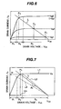
- Fig. 6 is a graph showing the current-voltage characteristics of the fuse circuit when the gate voltage V g of the selection transistor is changed.
- Fig. 7 is a graph showing the current-voltage characteristics of the fuse circuit.
- the power supply voltage is represented by V DD .
- a program voltage applied to the gate terminal of the selection transistor to break the fuse element is represented by V p .
- a line L indicates the current-voltage characteristics of a fuse element at the fuse resistance of Rf.
- the gate voltage Vg to be applied to the gate terminal of a selection transistor is raised from Vg1 to Vg2 and to Vg3, the drain current I D of the selection transistor increases.
- the cross point between the I-V characteristics of the selection transistor and the I-V characteristics of the fuse element also change from P1 to P2 and to P3.
- a difference voltage between the power supply voltage V DD and the drain voltage at the operating point P is a voltage applied across the fuse element. Therefore, as the gate voltage Vg is raised, the consumption power of the fuse element increases.
- the operating point P3 is used because a drain current sufficient for breaking down the fuse element can be obtained.
- the resistance value of the fuse element is selected so that the fuse element can be broken down in the state that the operating point P3 is in the transition region R3 between the linear region R1 and saturation region R2.
- the resistance value of the fuse element is set to such a value as a difference voltage between a second voltage (source voltage, in this example, ground potential) and the voltage at the node (connection point) between the fuse element and selection transistor is lower than the drain voltage at which the drain current of a MOS transistor starts saturating under the condition that a program voltage is applied to the gate terminal of the selection transistor. In this case, the ratio of invalid voltage not contributing to breaking down the fuse element can be lowered.
- the resistance value of the fuse element is set to such a value as a difference voltage between the second voltage and the voltage at the connection point between the fuse element and selection transistor is higher than the drain voltage in the linear region where the drain current of a MOS transistor is proportional to the drain voltage under the condition that a program voltage is applied to the gate terminal of the selection transistor.
- the drive ability of the MOS transistor can be utilized sufficiently and the size of the transistor can be made as small as necessary. The area occupied by the transistor can therefore be reduced.
- the fuse element is broken down in accordance with any one of the following setting methods.
- a first voltage is applied between opposite ends of a serial connection of a fuse element and a selection transistor, the first voltage being higher than a drain voltage at which a drain current of the selection transistor starts saturating.
- a predetermined program voltage is applied to the gate electrode of the selection transistor.
- the fuse element is broken down under the condition that a voltage at the connection point between the fuse element and selection transistor is higher than the drain voltage in the build-up linear region of the selection transistor and lower than the drain voltage in the saturation region.
Landscapes
- Design And Manufacture Of Integrated Circuits (AREA)
- Semiconductor Integrated Circuits (AREA)
- Read Only Memory (AREA)
Abstract
Description
Claims (8)
- A semiconductor device comprising:wherein:a fuse element capable of being electrically broken down by flowing current therethrough, a first voltage being applied to one end of said fuse element; anda MOS type transistor having source, gate and drain terminals and a connection point between the other end of said fuse element and one of the source and drain terminals, a second voltage lower than the first voltage being applied to the other of the source and drain terminals,the first and second voltages, characteristics of said MOS type transistor and a resistance value of said fuse element are selected so that said fuse element can be broken down when a predetermined program voltage is applied to the gate terminal; andthe resistance value of said fuse element is set to such a value as a voltage difference between a voltage at the connection point and the second voltage is lower than a drain voltage of said MOS type transistor at which a drain current starts saturating, when the program voltage is applied to the gate terminal,the resistance value of said fuse element is further set to such a value as a minimum power capable of breaking down said fuse element is not smaller than 90 % of a maximum consumption power of said fuse element calculated from current-voltage characteristics of said MOS type transistor, orthe resistance value of said fuse element is further set to such a value as a breakdown current of said fuse element is in a range from 80 % to 98 % of a saturation drain current of said MOS type transistor.
- A semiconductor device according to claim 1, wherein the resistance value of said fuse element is further set to such a value as a voltage difference between a voltage at the connection point and the second voltage is higher than the drain voltage in a linear region where the drain current of said MOS type transistor is proportional to the drain current, when the program voltage is applied to the gate terminal.
- A semiconductor device according to claim 1, wherein the program voltage of said MOS type transistor is approximately equal to the first voltage.
- A semiconductor device according to claim 1, wherein the gate terminal of said MOS type transistor and said fuse element are made of a same layer.
- A semiconductor device according to claim 1, wherein the same layer is made of polycide.
- A method of manufacturing a semiconductor device, comprising the steps of:forming on a substrate a serial connection of a fuse element and a MOS type transistor, the fuse element being capable of being electrically broken down by flowing current therethrough, and the MOS type transistor having source, gate and drain terminals and a connection point between one end of said fuse element and one of the source and drain terminals; andapplying a voltage higher than a drain voltage of the MOS type transistor at which a drain current starts saturation, between another end of the fuse element and the other of the source and drain terminals, applying a predetermined program voltage to the gate terminal, and breaking down the fuse element by setting a voltage at the connection point between the fuse element and the MOS type transistor to a voltage lower than a drain voltage of the MOS type transistor in a saturation region in which a drain current saturates, breaking down the fuse element by setting a voltage at the connection point of the MOS type transistor in a voltage range in which a consumption power of the fuse element is not smaller than 90 % of a maximum consumption power of the fuse element calculated from current-voltage characteristics of the MOS type transistor, or breaking down the fuse element by setting a voltage at the connection point between the fuse element and the MOS type transistor in a voltage range in which 80 % to 98 % of a saturation current of the MOS type transistor flows.
- A semiconductor device according to claim 1, wherein said resistance value of said fuse element is a value immediately before the fuse element is broken down.
- A method of manufacturing a semiconductor device according to claim 6, wherein said resistance value of said fuse element is a value immediately before the fuse element is broken down.
Applications Claiming Priority (2)
| Application Number | Priority Date | Filing Date | Title |
|---|---|---|---|
| JP2001340872 | 2001-11-06 | ||
| JP2001340872 | 2001-11-06 |
Publications (3)
| Publication Number | Publication Date |
|---|---|
| EP1309002A2 true EP1309002A2 (en) | 2003-05-07 |
| EP1309002A3 EP1309002A3 (en) | 2006-05-10 |
| EP1309002B1 EP1309002B1 (en) | 2012-01-11 |
Family
ID=19155012
Family Applications (1)
| Application Number | Title | Priority Date | Filing Date |
|---|---|---|---|
| EP02024929A Expired - Lifetime EP1309002B1 (en) | 2001-11-06 | 2002-11-06 | Semiconductor device having fuse and its manufacturing method |
Country Status (6)
| Country | Link |
|---|---|
| US (3) | US6804159B2 (en) |
| EP (1) | EP1309002B1 (en) |
| KR (1) | KR100539113B1 (en) |
| CN (1) | CN1305134C (en) |
| HK (1) | HK1052408B (en) |
| TW (1) | TWI235456B (en) |
Families Citing this family (30)
| Publication number | Priority date | Publication date | Assignee | Title |
|---|---|---|---|---|
| KR100718614B1 (en) * | 2003-10-24 | 2007-05-16 | 야마하 가부시키가이샤 | Semiconductor device with capacitor and fuse and its manufacturing method |
| US7026692B1 (en) * | 2003-11-12 | 2006-04-11 | Xilinx, Inc. | Low voltage non-volatile memory transistor |
| DE102004014925B4 (en) * | 2004-03-26 | 2016-12-29 | Infineon Technologies Ag | Electronic circuit arrangement |
| US7227239B2 (en) * | 2004-09-23 | 2007-06-05 | International Business Machines Corporation | Resettable fuse device and method of fabricating the same |
| US7193292B2 (en) * | 2004-12-02 | 2007-03-20 | Taiwan Semiconductor Manufacturing Co., Ltd | Fuse structure with charge protection circuit |
| US7442583B2 (en) * | 2004-12-17 | 2008-10-28 | International Business Machines Corporation | Using electrically programmable fuses to hide architecture, prevent reverse engineering, and make a device inoperable |
| CN100501973C (en) * | 2005-03-30 | 2009-06-17 | 雅马哈株式会社 | Fuse disconnection method suitable for semiconductor device |
| US7242239B2 (en) * | 2005-06-07 | 2007-07-10 | International Business Machines Corporation | Programming and determining state of electrical fuse using field effect transistor having multiple conduction states |
| JP2007004887A (en) * | 2005-06-23 | 2007-01-11 | Toshiba Corp | Semiconductor memory device |
| US7307880B2 (en) * | 2005-11-14 | 2007-12-11 | Taiwan Semiconductor Manufacturing Company, Ltd. | One time programming memory cell using MOS device |
| KR100790819B1 (en) * | 2006-07-20 | 2008-01-02 | 삼성전자주식회사 | Semiconductor integrated circuits and manufacturing method thereof |
| JP2008042108A (en) * | 2006-08-10 | 2008-02-21 | Hitachi Ltd | Semiconductor device |
| US8445362B2 (en) * | 2006-10-11 | 2013-05-21 | International Business Machines Corporation | Apparatus and method for programming an electronically programmable semiconductor fuse |
| KR100824879B1 (en) * | 2006-12-28 | 2008-04-23 | 동부일렉트로닉스 주식회사 | Semiconductor devices with fuses |
| US7888771B1 (en) | 2007-05-02 | 2011-02-15 | Xilinx, Inc. | E-fuse with scalable filament link |
| JP2009177044A (en) * | 2008-01-28 | 2009-08-06 | Panasonic Corp | Electrical fuse circuit |
| US7710813B1 (en) | 2008-03-05 | 2010-05-04 | Xilinx, Inc. | Electronic fuse array |
| US7834659B1 (en) | 2008-03-05 | 2010-11-16 | Xilinx, Inc. | Multi-step programming of E fuse cells |
| US7724600B1 (en) | 2008-03-05 | 2010-05-25 | Xilinx, Inc. | Electronic fuse programming current generator with on-chip reference |
| US8564023B2 (en) * | 2008-03-06 | 2013-10-22 | Xilinx, Inc. | Integrated circuit with MOSFET fuse element |
| US7923811B1 (en) | 2008-03-06 | 2011-04-12 | Xilinx, Inc. | Electronic fuse cell with enhanced thermal gradient |
| CN102270497A (en) * | 2010-06-02 | 2011-12-07 | 王彬 | Memory utilizing shadow nonvolatile memory configured with redundancy storage |
| DE102011010567A1 (en) * | 2011-02-07 | 2012-08-09 | Magna Electronics Europe Gmbh & Co.Kg | Brushless DC motor |
| US20120286390A1 (en) * | 2011-05-11 | 2012-11-15 | Kuei-Sheng Wu | Electrical fuse structure and method for fabricating the same |
| US10438836B2 (en) | 2011-11-09 | 2019-10-08 | Unisantis Electronics Singapore Pte. Ltd. | Method for manufacturing a semiconductor device |
| US8759178B2 (en) | 2011-11-09 | 2014-06-24 | Unisantis Electronics Singapore Pte. Ltd. | Method for manufacturing semiconductor device and semiconductor device |
| CN103178824A (en) * | 2013-03-18 | 2013-06-26 | 西安华芯半导体有限公司 | Integrated circuit with partial module power shutoff function and shutoff method |
| CN110830022B (en) * | 2018-08-10 | 2023-08-25 | 圣邦微电子(北京)股份有限公司 | Trimming circuit and chip |
| CN113096717B (en) * | 2020-01-08 | 2024-02-27 | 中芯国际集成电路制造(上海)有限公司 | Fuse memory cell, memory array and working method of memory array |
| CN117519396B (en) * | 2023-12-27 | 2024-03-22 | 中国科学院合肥物质科学研究院 | Load self-adaptive high-efficiency pulse constant current source and control method |
Family Cites Families (9)
| Publication number | Priority date | Publication date | Assignee | Title |
|---|---|---|---|---|
| US4441167A (en) * | 1981-12-03 | 1984-04-03 | Raytheon Company | Reprogrammable read only memory |
| JPS63299139A (en) * | 1987-05-28 | 1988-12-06 | Nec Corp | Method of melting fuse |
| JPH0793030B2 (en) * | 1990-04-06 | 1995-10-09 | 株式会社東芝 | Semiconductor memory device |
| EP0684677B1 (en) * | 1993-02-10 | 2003-12-17 | Line Electronics Corporation | Overcurrent protective circuit and semiconductor device |
| KR0122103B1 (en) * | 1994-05-07 | 1997-11-26 | 김광호 | The fuse device of a semiconductor memory equipment |
| KR0145888B1 (en) * | 1995-04-13 | 1998-11-02 | 김광호 | Operation mode switching circuit of semiconductor memory device |
| KR0157345B1 (en) * | 1995-06-30 | 1998-12-01 | 김광호 | Electric cell for semiconductor memory |
| JP3176324B2 (en) * | 1997-07-29 | 2001-06-18 | 日本電気アイシーマイコンシステム株式会社 | Semiconductor integrated circuit |
| JP2002134620A (en) * | 2000-10-27 | 2002-05-10 | Mitsubishi Electric Corp | Semiconductor device |
-
2002
- 2002-11-06 US US10/288,493 patent/US6804159B2/en not_active Expired - Lifetime
- 2002-11-06 CN CNB021502366A patent/CN1305134C/en not_active Expired - Fee Related
- 2002-11-06 EP EP02024929A patent/EP1309002B1/en not_active Expired - Lifetime
- 2002-11-06 KR KR10-2002-0068381A patent/KR100539113B1/en not_active Expired - Fee Related
- 2002-11-06 TW TW091132855A patent/TWI235456B/en not_active IP Right Cessation
-
2003
- 2003-06-24 HK HK03104525.3A patent/HK1052408B/en not_active IP Right Cessation
-
2004
- 2004-09-08 US US10/935,426 patent/US7248529B2/en not_active Expired - Fee Related
- 2004-12-20 US US11/015,030 patent/US7180810B2/en not_active Expired - Fee Related
Also Published As
| Publication number | Publication date |
|---|---|
| CN1305134C (en) | 2007-03-14 |
| CN1419289A (en) | 2003-05-21 |
| HK1052408A1 (en) | 2003-09-11 |
| US7180810B2 (en) | 2007-02-20 |
| EP1309002B1 (en) | 2012-01-11 |
| KR100539113B1 (en) | 2005-12-26 |
| US20050099860A1 (en) | 2005-05-12 |
| HK1052408B (en) | 2007-06-08 |
| KR20030038457A (en) | 2003-05-16 |
| TW200301956A (en) | 2003-07-16 |
| US6804159B2 (en) | 2004-10-12 |
| US7248529B2 (en) | 2007-07-24 |
| US20050029621A1 (en) | 2005-02-10 |
| EP1309002A3 (en) | 2006-05-10 |
| TWI235456B (en) | 2005-07-01 |
| US20030122200A1 (en) | 2003-07-03 |
Similar Documents
| Publication | Publication Date | Title |
|---|---|---|
| US6804159B2 (en) | Semiconductor device having fuse and its manufacture method | |
| US20080277729A1 (en) | Electrostatic discharge protection element | |
| US6963100B2 (en) | Semiconductor device having gate electrode in which depletion layer can be generated | |
| US6222710B1 (en) | Semiconductor device | |
| JP2000208610A (en) | Insulated transistor with adjustable threshold | |
| US5834813A (en) | Field-effect transistor for one-time programmable nonvolatile memory element | |
| EP0700090A1 (en) | Semiconductor integrated circuit comprising a current mirror circuit | |
| US7259951B2 (en) | Semiconductor device | |
| EP0601823B1 (en) | Method of forming a field effect transistor with integrated schottky diode clamp | |
| JP2839375B2 (en) | Semiconductor integrated circuit device | |
| US8525251B2 (en) | Nonvolatile programmable logic switch | |
| JP3948392B2 (en) | Semiconductor device, semiconductor device manufacturing method, and fuse element cutting method | |
| US20040256681A1 (en) | Semiconductor protection element, semiconductor device and method for manufacturing same | |
| US5570311A (en) | SRAM semiconductor device | |
| US20210351192A1 (en) | One-time programmable device with antifuse | |
| JP2004228317A (en) | Semiconductor storage device | |
| US7518167B2 (en) | Semiconductor device | |
| JPH07202009A (en) | Semiconductor device having output circuit of cmos structure | |
| JP2008091936A (en) | Semiconductor device | |
| KR20000051373A (en) | Electric fuse for using memory chip | |
| JP2008277846A (en) | Semiconductor device |
Legal Events
| Date | Code | Title | Description |
|---|---|---|---|
| PUAI | Public reference made under article 153(3) epc to a published international application that has entered the european phase |
Free format text: ORIGINAL CODE: 0009012 |
|
| AK | Designated contracting states |
Designated state(s): AT BE BG CH CY CZ DE DK EE ES FI FR GB GR IE IT LI LU MC NL PT SE SK TR |
|
| AX | Request for extension of the european patent |
Extension state: AL LT LV MK RO SI |
|
| PUAL | Search report despatched |
Free format text: ORIGINAL CODE: 0009013 |
|
| AK | Designated contracting states |
Kind code of ref document: A3 Designated state(s): AT BE BG CH CY CZ DE DK EE ES FI FR GB GR IE IT LI LU MC NL PT SE SK TR |
|
| AX | Request for extension of the european patent |
Extension state: AL LT LV MK RO SI |
|
| 17P | Request for examination filed |
Effective date: 20061107 |
|
| AKX | Designation fees paid |
Designated state(s): DE FR GB |
|
| 17Q | First examination report despatched |
Effective date: 20070222 |
|
| RAP1 | Party data changed (applicant data changed or rights of an application transferred) |
Owner name: YAMAHA CORPORATION |
|
| GRAP | Despatch of communication of intention to grant a patent |
Free format text: ORIGINAL CODE: EPIDOSNIGR1 |
|
| GRAS | Grant fee paid |
Free format text: ORIGINAL CODE: EPIDOSNIGR3 |
|
| GRAA | (expected) grant |
Free format text: ORIGINAL CODE: 0009210 |
|
| AK | Designated contracting states |
Kind code of ref document: B1 Designated state(s): DE FR GB |
|
| REG | Reference to a national code |
Ref country code: GB Ref legal event code: FG4D |
|
| REG | Reference to a national code |
Ref country code: DE Ref legal event code: R096 Ref document number: 60241935 Country of ref document: DE Effective date: 20120308 |
|
| PLBE | No opposition filed within time limit |
Free format text: ORIGINAL CODE: 0009261 |
|
| STAA | Information on the status of an ep patent application or granted ep patent |
Free format text: STATUS: NO OPPOSITION FILED WITHIN TIME LIMIT |
|
| 26N | No opposition filed |
Effective date: 20121012 |
|
| REG | Reference to a national code |
Ref country code: DE Ref legal event code: R097 Ref document number: 60241935 Country of ref document: DE Effective date: 20121012 |
|
| PGFP | Annual fee paid to national office [announced via postgrant information from national office to epo] |
Ref country code: GB Payment date: 20141105 Year of fee payment: 13 Ref country code: FR Payment date: 20141110 Year of fee payment: 13 Ref country code: DE Payment date: 20141029 Year of fee payment: 13 |
|
| REG | Reference to a national code |
Ref country code: DE Ref legal event code: R119 Ref document number: 60241935 Country of ref document: DE |
|
| GBPC | Gb: european patent ceased through non-payment of renewal fee |
Effective date: 20151106 |
|
| REG | Reference to a national code |
Ref country code: FR Ref legal event code: ST Effective date: 20160729 |
|
| PG25 | Lapsed in a contracting state [announced via postgrant information from national office to epo] |
Ref country code: DE Free format text: LAPSE BECAUSE OF NON-PAYMENT OF DUE FEES Effective date: 20160601 Ref country code: GB Free format text: LAPSE BECAUSE OF NON-PAYMENT OF DUE FEES Effective date: 20151106 |
|
| PG25 | Lapsed in a contracting state [announced via postgrant information from national office to epo] |
Ref country code: FR Free format text: LAPSE BECAUSE OF NON-PAYMENT OF DUE FEES Effective date: 20151130 |