EP1308977B1 - Electrostatic actuator, and electrostatic microrelay and other devices using the same - Google Patents
Electrostatic actuator, and electrostatic microrelay and other devices using the same Download PDFInfo
- Publication number
- EP1308977B1 EP1308977B1 EP02102543A EP02102543A EP1308977B1 EP 1308977 B1 EP1308977 B1 EP 1308977B1 EP 02102543 A EP02102543 A EP 02102543A EP 02102543 A EP02102543 A EP 02102543A EP 1308977 B1 EP1308977 B1 EP 1308977B1
- Authority
- EP
- European Patent Office
- Prior art keywords
- electrode
- insulating film
- electrostatic actuator
- electrostatic
- film
- Prior art date
- Legal status (The legal status is an assumption and is not a legal conclusion. Google has not performed a legal analysis and makes no representation as to the accuracy of the status listed.)
- Expired - Lifetime
Links
- 150000004767 nitrides Chemical class 0.000 claims abstract description 51
- 239000000463 material Substances 0.000 claims abstract description 17
- 238000000926 separation method Methods 0.000 claims description 3
- VYPSYNLAJGMNEJ-UHFFFAOYSA-N Silicium dioxide Chemical compound O=[Si]=O VYPSYNLAJGMNEJ-UHFFFAOYSA-N 0.000 abstract description 3
- 229910052681 coesite Inorganic materials 0.000 abstract 1
- 229910052906 cristobalite Inorganic materials 0.000 abstract 1
- 239000000377 silicon dioxide Substances 0.000 abstract 1
- 235000012239 silicon dioxide Nutrition 0.000 abstract 1
- 229910052682 stishovite Inorganic materials 0.000 abstract 1
- 229910052905 tridymite Inorganic materials 0.000 abstract 1
- 239000000758 substrate Substances 0.000 description 39
- 238000012546 transfer Methods 0.000 description 16
- 239000002184 metal Substances 0.000 description 13
- 229910052751 metal Inorganic materials 0.000 description 13
- 238000000034 method Methods 0.000 description 13
- 238000004519 manufacturing process Methods 0.000 description 11
- 238000012360 testing method Methods 0.000 description 10
- 230000005684 electric field Effects 0.000 description 9
- 239000011521 glass Substances 0.000 description 9
- 150000002500 ions Chemical class 0.000 description 7
- 230000000694 effects Effects 0.000 description 6
- 239000012212 insulator Substances 0.000 description 6
- 230000008569 process Effects 0.000 description 6
- 230000005540 biological transmission Effects 0.000 description 5
- 230000008859 change Effects 0.000 description 5
- 238000005530 etching Methods 0.000 description 5
- 238000012545 processing Methods 0.000 description 5
- 239000004020 conductor Substances 0.000 description 4
- 238000004544 sputter deposition Methods 0.000 description 4
- 150000001450 anions Chemical class 0.000 description 3
- 238000005452 bending Methods 0.000 description 3
- 230000015572 biosynthetic process Effects 0.000 description 3
- 230000015556 catabolic process Effects 0.000 description 3
- 238000006731 degradation reaction Methods 0.000 description 3
- 239000011810 insulating material Substances 0.000 description 3
- 230000002093 peripheral effect Effects 0.000 description 3
- 230000009467 reduction Effects 0.000 description 3
- 229910052581 Si3N4 Inorganic materials 0.000 description 1
- 230000004913 activation Effects 0.000 description 1
- 239000000853 adhesive Substances 0.000 description 1
- 230000001070 adhesive effect Effects 0.000 description 1
- 230000008901 benefit Effects 0.000 description 1
- 239000000872 buffer Substances 0.000 description 1
- 230000003139 buffering effect Effects 0.000 description 1
- 150000001768 cations Chemical class 0.000 description 1
- 230000001413 cellular effect Effects 0.000 description 1
- 239000011248 coating agent Substances 0.000 description 1
- 238000000576 coating method Methods 0.000 description 1
- 239000000470 constituent Substances 0.000 description 1
- 230000008878 coupling Effects 0.000 description 1
- 238000010168 coupling process Methods 0.000 description 1
- 238000005859 coupling reaction Methods 0.000 description 1
- 238000010494 dissociation reaction Methods 0.000 description 1
- 230000005593 dissociations Effects 0.000 description 1
- 238000010292 electrical insulation Methods 0.000 description 1
- 239000007772 electrode material Substances 0.000 description 1
- 230000003116 impacting effect Effects 0.000 description 1
- 238000002347 injection Methods 0.000 description 1
- 239000007924 injection Substances 0.000 description 1
- 238000009413 insulation Methods 0.000 description 1
- 238000005304 joining Methods 0.000 description 1
- 238000005259 measurement Methods 0.000 description 1
- 239000012528 membrane Substances 0.000 description 1
- 150000002739 metals Chemical class 0.000 description 1
- 238000005459 micromachining Methods 0.000 description 1
- 238000012544 monitoring process Methods 0.000 description 1
- 239000011295 pitch Substances 0.000 description 1
- 230000010287 polarization Effects 0.000 description 1
- 239000003566 sealing material Substances 0.000 description 1
- 230000008054 signal transmission Effects 0.000 description 1
- 229910052710 silicon Inorganic materials 0.000 description 1
- 239000010703 silicon Substances 0.000 description 1
- HQVNEWCFYHHQES-UHFFFAOYSA-N silicon nitride Chemical compound N12[Si]34N5[Si]62N3[Si]51N64 HQVNEWCFYHHQES-UHFFFAOYSA-N 0.000 description 1
- 229910052814 silicon oxide Inorganic materials 0.000 description 1
- 239000000243 solution Substances 0.000 description 1
- 230000003068 static effect Effects 0.000 description 1
Images












Classifications
-
- H—ELECTRICITY
- H01—ELECTRIC ELEMENTS
- H01H—ELECTRIC SWITCHES; RELAYS; SELECTORS; EMERGENCY PROTECTIVE DEVICES
- H01H59/00—Electrostatic relays; Electro-adhesion relays
- H01H59/0009—Electrostatic relays; Electro-adhesion relays making use of micromechanics
-
- H—ELECTRICITY
- H01—ELECTRIC ELEMENTS
- H01H—ELECTRIC SWITCHES; RELAYS; SELECTORS; EMERGENCY PROTECTIVE DEVICES
- H01H59/00—Electrostatic relays; Electro-adhesion relays
-
- H—ELECTRICITY
- H01—ELECTRIC ELEMENTS
- H01H—ELECTRIC SWITCHES; RELAYS; SELECTORS; EMERGENCY PROTECTIVE DEVICES
- H01H1/00—Contacts
- H01H1/0036—Switches making use of microelectromechanical systems [MEMS]
- H01H2001/0084—Switches making use of microelectromechanical systems [MEMS] with perpendicular movement of the movable contact relative to the substrate
-
- H—ELECTRICITY
- H01—ELECTRIC ELEMENTS
- H01H—ELECTRIC SWITCHES; RELAYS; SELECTORS; EMERGENCY PROTECTIVE DEVICES
- H01H59/00—Electrostatic relays; Electro-adhesion relays
- H01H59/0009—Electrostatic relays; Electro-adhesion relays making use of micromechanics
- H01H2059/0018—Special provisions for avoiding charge trapping, e.g. insulation layer between actuating electrodes being permanently polarised by charge trapping so that actuating or release voltage is altered
-
- H—ELECTRICITY
- H01—ELECTRIC ELEMENTS
- H01H—ELECTRIC SWITCHES; RELAYS; SELECTORS; EMERGENCY PROTECTIVE DEVICES
- H01H59/00—Electrostatic relays; Electro-adhesion relays
- H01H59/0009—Electrostatic relays; Electro-adhesion relays making use of micromechanics
- H01H2059/0072—Electrostatic relays; Electro-adhesion relays making use of micromechanics with stoppers or protrusions for maintaining a gap, reducing the contact area or for preventing stiction between the movable and the fixed electrode in the attracted position
Definitions
- the present invention relates to an electrostatic actuator, an electrostatic micro-relay and other devices using the same.
- Fig. 1 is an exploded perspective view that shows a structure of a conventional electrostatic actuator and Fig. 2 shows a cross-sectional view thereof.
- This electrostatic actuator 1 which is disclosed in Japanese Laid-Open Patent Application No. 2000-164104 , is mainly constituted by a fixed substrate 2 and a movable substrate 3.
- the fixed substrate 2 is made of a glass substrate having a fixed electrode 4 and a pair of fixed contacts 5, 6 formed on the upper face thereof.
- the surface of the fixed electrode 4 is coated with an insulating film 7 made from an oxide.
- the fixed contacts 5, 6 are respectively connected to connection pads 10, 11 on the fixed substrate 2 through respective wires 8, 9.
- the movable substrate 3 made from an Si substrate is provided with a movable electrode 13 supported by four elastic beams 12 in the center portion thereof, and a movable contact 15 is placed on the center portion of the lower face of the movable electrode 13 through an insulating layer 14.
- An anchor 16 protrudes from a peripheral portion of the lower face of the movable substrate 3 so that, when the movable substrate 3 is fixed on the upper face of the fixed substrate 2 by the anchor 16, the movable electrode 13 and the fixed electrode 4 are aligned face to face with each other with a space in between; thus, the movable contact 15 is aligned face to face with the fixed contacts 5, 6 with a space in between in a manner so as to bridge a space between the fixed contacts 5 and 6.
- the movable electrode 13 when a driving voltage, applied between the fixed electrode 4 and the movable electrode 13, has reached a predetermined voltage value, the movable electrode 13 is attracted toward the fixed electrode 4 side by an electrostatic attracting force that is exerted between the fixed electrode 4 and the movable electrode 13 so that the movable electrode 13 is allowed to adhere to the fixed electrode 4 through the insulating film 7 with the elastic beam 12 being distorted.
- the movable contact 15 is pressed between the fixed contacts 5 and 6 so that the fixed contacts 5, 6 are electrically closed by the movable contact 15 so that a pair of connection pads 10 and 11 are allowed to conduct to each other.
- Patent US-A-6,162,657 (D1) discloses in relation to figures 12-19 a micromechanical relay, comprising: a mobile electrode (39, 139) and a fixed electrode (180, 190, 280, 380) facing each other.
- the mobile electrode (39, 139) carries a contact bridge 40.
- Said contact bridge 40 is for establishing an electrical contact between two contact pads 44 and 46. When a voltage is applied between the fixed and mobiles electrodes, the mobile electrode is attracted toward the fixed one. Then the bridge 40 establishes contact between contact pads 44, 46.
- an insulating layer 50 is provided so as to prevent possible contacting between the contact bridge 40 and the fixed electrode (180, 190, 280, 380).
- the insulating film (50) is formed on a face of the first electrode (39) at an area where the first electrode (39) and the second electrode (280) are face to face to one another.
- An object of US-A-6,162,657 is to prevent permanent sticking of the mobile electrode 39, 139 of the micromechanical relay to the fixed electrode when the micromechanical relay is in operation.
- the adhesive forces between the movable electrode 39, 139, and the fixed electrode are reduced, by reducing the contact surface between the two electrodes.
- the reduction of the contact surface is achieved through roughing of the fixed electrode as described in relation to figures 12, 13, or by providing the surface of the fixed electrode with depressions and elevations as shown in figures 14-16 or by etching pyramids on said surface of the fixed electrode as shown in figures 17-19.
- EP-A-0 709 911 discloses micromechanical microwaves micro-switches.
- a preferred embodiment is described in relation to figures 4a-4e.
- Said embodiment comprises: a first electrode 415 made of a metal film coated with a dielectric layer 412.
- the electrode 415 is in two parts.
- a second electrode in two parts 405, 406 is disposed face to face with the first electrode 415.
- the dielectric insulating film 412 is between the first and second electrodes.
- a metal plate 414 is disposed on the film 412. Two ends 402, 403 of a transmission lines are facing metal plate 414.
- Impedance of said capacity for microwave is small enough to be negligible, there is connection, capacitive coupling, between ends 402, 403 of the transmission line. It is indicated that a leaky dielectric 412 should be used to avoid static charge build up in said dielectric, which would act as an activation charge. It is also indicated that the thickness of membrane 412 and metal film 415 provide a tradeoff of the electrode threshold voltage required to pull down and the restoring force required for pull up.
- US-6,307,452 discloses in relation with figures 5 and 6 a micro electromechanical switch 10 built on a substrate 12.
- the switch comprises top and bottom control electrode 14, 16 disposed face to face.
- An actuating portion contains a micro platform structure 20, which is suspended over a gap 21 by means of four springs 22.
- the micro platform 20 is composed of two bimorph layers including an electrical insulation layer and an electrically conductive film.
- the dielectric insulation layer acts as a main mechanical structure material while the conductive material acts as the electrostatic control top electrodes 16.
- An electrical contact 32 is formed on a signal line 18.
- the contact 32 is positioned on the signal line to face a shorting bar 34 of the micro platform 20.
- switch 10 is normally in a "off" position.
- the switch 10 When the switch 10 is in the "off” position, the signal line 18 is an open circuit due to gap 21 and the separation of the signal lines 18.
- the switch 10 is actuated to an "on” position by applying a voltage to the top electrode 16. With a voltage on top electrode 16, electrostatic forces attract the platform 20 toward the bottom electrode 14 causing the shorting bar 34 with the contact post 32 to thereby close the gap 21 and place the signal line 18 in the "on” state.
- landing bumpers 26 are positioned beneath each of the four springs 22 near the micro platform 20. The bumpers 26 are symmetrically positioned directly beneath the springs at near the point where each spring is connected to the corner of the micro platform 20.
- the landing bumpers support the micro platform 20 when the micro platform 20 is moved to an "on" state such that a relatively small area of contact is made between the micro platform 20 and the bottom electrode 14. Stiction problems due to the physical contact between the micro platform 20 and the bottom electrode 14 is dramatically reduced. Then the micro platform 20 is moved to the "on" position, mechanical impact against the substrate 12 occurs so that the landing bumpers 26 which are positioned outside the bottom electrode 14 functional area are used as mechanical buffers to prevent the micro platform 20 from directly impacting against the bottom electrode 14. The landing bumpers 26 further reduce the stiction from the charge injection into the dielectric layer of the platform.
- Patent US-A-5 367 429 D4 discloses an electrostatic type micro transducer such as a micro sensor and micro actuator comprising control electrodes 5 and 6 facing one another.
- An object of US-A-5 367 429 is to provide an electrostatic type micro transducer having means, which prevents sticking between a movable electrode and a stationary electrode, which may render the electrostatic type micro transducer inoperable.
- a horizontal protrusion 7a is provided for respective insulator films 7 located at the top end on the movable control electrode 5.
- the respective horizontal protrusions 7a are adapted to contact initially to one of stationary control electrodes 6 to thereby prevent the contacting between the movable electrode 5 and one of the stationary electrodes 6.
- the top end of the movable electrode 5 is formed in a taper shape via inclined surfaces 5a, the distance between the possible contacting portion of a horizontal protrusion 7a on the stationary electrode 6 and the movable electrode 5, in that the inclined surface 5a increases, thereby the electrical field strength near the insulating films 7 is reduced when the movable electrode 5 contacts to one of the stationary electrodes 6 via the insulator films 7. Accordingly, after the electric field is removed residual dielectric polarization and residual electric charges in the insulator films 7 are sufficiently reduced and the sticking between the electrodes is eliminated.
- Fig. 3 the CV characteristic of the electrostatic actuator is represented by the relationship between a driving voltage Vdrive applied between the fixed electrode 4 and the movable electrode 13 and a capacitance C between the two electrodes 4 and 13.
- Vdrive applied between the fixed electrode 4 and the movable electrode 13
- C capacitance
- C1 represents a value of the capacitance C in a state where no driving voltage is applied between the movable electrode 13 and the fixed electrode 4
- C2 represents a value of the capacitance C in a state where the movable electrode 13 adheres to the fixed electrode 4 through the insulating film 7
- on-voltage Von is a value of the driving voltage Vdrive at the time when the movable electrode 13 is made to adhere to the fixed electrode 4 (or is released from the fixed electrode 4)
- the ways of charging are classified into two ways. Here, these ways are respectively referred to as a plus shift and a minus shift.
- the plus shift refers to a charging in which the center value of the CV characteristic is shifted toward the plus side of the driving voltage (see Fig. 6).
- the cause of the plus shift is that a charge transfer (transfer of charge) occurs at a portion on which the insulating film on the fixed electrode and the movable electrode come into contact with each other with the result that the insulating film is charged.
- the charge transfer is a phenomenon in which, when the contact portion of an insulator and a conductor is subjected to an electric field and heat, a charge is accumulated in the insulator, thereby charging the insulator.
- the minus shift refers to a charging in which the center value of the CV characteristic is shifted toward the minus side of the driving voltage (see Fig. 6).
- the minus shift is caused by an ionic charging. In other words, this is caused by the fact that ions, generated in processes such as an anodic bonding, are diffused in the insulating film of the oxide so that positive and negative ions diffused in the insulating film are shifted by an electric field applied between the movable electrode and the fixed electrode toward the mutually opposite sides.
- Vapp Vdrive + ⁇ Vn , with the result that the apparent on-voltage is lowered to Von - ⁇ Vn (here, Von is a value of the on-voltage in the case of no charge).
- the problem with the minus shift is exerted as a decrease in the minimum driving voltage (apparent on-voltage) to be used for opening the fixed contacts, with the result that, even when the driving voltage Vdrive is set to 0 volt, the electrostatic actuator fails to turn off or hardly turns off (that is, the electrostatic actuator is stuck, or susceptible to sticking).
- Fig. 6 shows a change in the CV characteristic before and after a thermal endurance test carried out on an electrostatic actuator.
- the CV characteristic F0 indicated by broken lines and rhomboidal shape points in Fig. 6, represents an initial characteristic prior to the conduction of the thermal endurance test, which shows a characteristic that is symmetrical with the driving voltage Vdrive.
- the present invention relates to an electrostatic actuator which is provided with means for controlling charging phenomena such as plus shift and minus shift so that it becomes possible to control operational voltage characteristics such as on-voltage and off-voltage.
- the present invention provides an electrostatic micro-relay using the above-mentioned electrostatic actuator and other devices.
- an electrostatic actuator of the present invention is provided with: a first electrode and a second electrode that are placed face to face with each other; and an insulating film that is formed on an opposing face of at least one electrode of the two electrodes at an area where the first electrode and the second electrode are made face to face with each other so that at least one of the first electrode and the second electrode is driven by an electrostatic force that is exerted when a voltage is applied between the first electrode and second electrode to allow the first electrode and second electrode to contact each other with the insulating film being interpolated in between, and in this arrangement, at least one of the first electrode and second electrode has a structure for controlling charge quantity.
- the charge-quantity controlling structure since the charge-quantity controlling structure is provided, it is possible to control the quantities of positive and negative charges in the insulating film. For example, it becomes possible to reduce the quantity of a positive or negative charge caused by, for example, charge transfer and the like, or it becomes possible to reduce the quantity of a positive or negative charge caused by ionic charging and the like. As a result, it is possible to control the operational voltage characteristics such as on-voltage and off-voltage of the electrostatic actuator by controlling the charging phenomena such as plus shift and minus shift.
- the above-mentioned charge-quantity controlling structure has such an arrangement that the quantities of positive and negative charges, exerted when a voltage is applied between the first and second electrodes, are respectively controlled so that the sum of the quantities of charge in the insulating film is controlled.
- the quantity of positive charge and the quantity of negative charge are mutually cancelled so that the entire charge quantity (total quantity) generated in the insulating film is controlled.
- the thickness of the insulating film is adjusted so that the charge quantity in the insulating film is controlled.
- the thickness of the insulating layer in particular, the thickness of the oxide film
- the quantity of positive or negative charge of the insulating film due to, for example, ionic charging can be controlled.
- the charge quantity in the insulating film is preferably controlled based upon the thickness of a layer that is directly made in contact with the first electrode or the second electrode.
- the insulating film comprises an oxide film and a nitride film; thus, another effect for reducing the charge quantity due to ionic charging is obtained, and it becomes possible to optimize the manufacturing processes and consequently to manufacture an electrostatic actuator easily with high yield.
- the nitride film has a property of hardly transmitting ions, and since the application of a nitride film makes it possible to reduce the thickness of the oxide film while a proper voltage-resistant property is maintained, it becomes possible to reduce the charge quantity in the insulating film due to the ionic charging.
- the film is formed as a silicon oxide film or a silicon nitride film so that it becomes possible to manufacture an electrostatic actuator easily with high yield.
- the surface of the above-mentioned nitride film is preferably coated with the above-mentioned oxide film.
- the nitride film surface on the side opposite to the electrode fixing the insulating film is preferably covered with the oxide film.
- the nitride film is susceptible to damages upon manufacturing, causing degradation in the processing precision; however, it is possible to prevent damages to the nitride film by coating the nitride film with the oxide film.
- the above-mentioned insulating layer may be formed by a single material.
- the formation of the insulating film using a single material makes it possible to simplify the structure of the insulating film, and consequently to easily manufacture the insulating film.
- the charge quantity in the insulating film is controlled by adjusting a contact area of the two electrodes through the insulating film, in the area on which the first electrode and the second electrode are aligned face to face with each other.
- the contact area of the two electrodes with each other through the insulating film it is possible to control the quantity of positive or negative charge of the insulating film due to, for example, a charge transfer.
- At least one protrusion may be formed on at least one of the surfaces of the electrodes in which the contact with the other electrode is made through the film; thus, it is possible to control the entire contact area of the portion in which the contact through the film are made by using the protrusion (for example, the number and the respective contact areas of the protrusions).
- the surface of this protrusion is preferably formed into a spherical shape. The formation of the surface of the protrusion into a spherical shape makes it possible to reduce the contact area to the other electrode, and consequently to reduce the charge quantity due to a charge transfer effectively; thus, it is also possible to increase the space filling rate, and to strengthen the electrostatic force between the two electrodes.
- one portion of one of the first and second electrodes at least is not facing a portion of the other one of the first and second electrodes.
- the first electrode is formed in a plurality of post- shaped or line shaped fixed electrodes that are separated from each other by intervals.
- the first electrode is formed in a plurality of post-shaped or line shaped fixed electrodes that are separated from each other by intervals.
- a plurality of post shaped or line shaped protrusions are formed on the lower face of the movable electrode or on top of an insulating film formed on the first electrode and said protrusions are not facing the fixed electrodes.
- An electrostatic actuator according to embodiments of the present invention may be applied to an electrostatic micro-relay.
- this electrostatic micro-relay it is possible to transmit dc currents as well as high-frequency signals with low loss, and consequently to maintain a stable characteristic for a long time.
- an electrostatic actuator may be applied to various devices; and examples thereof include a radio device in which the electrostatic micro-relay is installed so as to open and close an electric signal between the antenna and the inner circuit, a measuring device in which the electrostatic micro-relay is installed so as to open and close an electric signal between a measuring subject and the inner circuit, and a personal digital assistance in which the electrostatic micro-relay is installed so as to open and close the inner electric signal.
- a radio device in which the electrostatic micro-relay is installed so as to open and close an electric signal between the antenna and the inner circuit
- a measuring device in which the electrostatic micro-relay is installed so as to open and close an electric signal between a measuring subject and the inner circuit
- a personal digital assistance in which the electrostatic micro-relay is installed so as to open and close the inner electric signal.
- Fig. 1 shows an exploded perspective view that indicates a structure of a conventional electrostatic actuator.
- Fig. 2 shows a cross-sectional view of the conventional electrostatic actuator.
- Fig. 3 shows a drawing that indicates a CV characteristic of an optimal electrostatic actuator.
- Fig. 4 shows a schematic drawing that explains a state in which a plus-shift charge is generated between a movable electrode and an insulating film.
- Fig. 5 shows a schematic drawing that indicates a state in which a minus-shift charge is generated in an insulating film.
- Fig. 6 shows a drawing that indicates a change in the CV characteristic before and after a thermal endurance test.
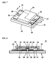
- Fig. 7 shows a perspective view of an electrostatic actuator in accordance with one embodiment of the present invention.
- Fig. 8 shows a cross-sectional view taken along line X-X of Fig. 7.
- Fig. 9 shows an exploded perspective view that indicates a structure of the electrostatic actuator of Fig. 7.
- Fig. 10 shows a schematic cross-sectional view that indicates a structure of an insulating film formed on a fixed electrode in the electrostatic actuator of Fig. 7.
- Fig. 11 shows a schematic drawing that indicates a principle, which suppresses the plus shift by forming a protrusion on the insulating film.
- Fig. 12 shows a schematic drawing that indicates a principle which suppresses the minus shift by forming a nitride film in the insulating film.
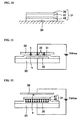
- Fig. 13 shows a schematic cross-sectional view that indicates an electrostatic actuator having another structure in accordance with the present invention.
- Fig. 14 shows a schematic cross-sectional view that indicates an electrostatic actuator having still another structure in accordance with the present invention.
- Fig. 15 shows a schematic cross-sectional view that indicates an electrostatic actuator having still another structure in accordance with the present invention.
- Fig. 16 shows a schematic cross-sectional view that indicates an electrostatic actuator having still another structure in accordance with the present invention.
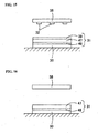
- Fig. 17 shows a schematic cross-sectional view that indicates an electrostatic actuator having still another structure in accordance with the present invention.
- Fig. 18 shows a schematic cross-sectional view that indicates an electrostatic actuator having still another structure in accordance with the present invention.
- Fig. 19 shows a schematic cross-sectional view that indicates an electrostatic actuator having still another structure in accordance with the present invention.
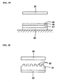
- Fig. 20 shows a schematic cross-sectional view that indicates an electrostatic actuator having still another structure in accordance with the present invention.
- Fig. 21 shows a schematic cross-sectional view that indicates an electrostatic actuator having still another structure in accordance with the present invention.
- Fig. 22 shows a schematic cross-sectional view that indicates an electrostatic actuator having still another structure in accordance with the present invention.
- Fig. 23 shows a schematic cross-sectional view that indicates an electrostatic actuator having still another structure in accordance with the present invention.
- Fig. 24 shows a schematic cross-sectional view that indicates an electrostatic actuator having still another structure in accordance with the present invention.
- Fig. 25 shows a schematic cross-sectional view that indicates an electrostatic actuator having still another structure in accordance with the present invention.
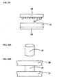
- Fig. 26A shows a perspective view that indicates a protrusion having a cylinder shape
- Fig. 26B shows a schematic drawing that explains a state in which the protrusion occupies a space between the insulating film and the movable electrode.
- Fig. 27A shows a perspective view that indicates a protrusion having a cone shape
- Fig. 27B shows a schematic drawing that explains a state in which the protrusion occupies a space between the insulating film and the movable electrode.
- Fig. 28A shows a perspective view that indicates a protrusion having a spherical shape
- Fig. 28B shows a schematic drawing that explains a state in which the protrusion occupies a space between the insulating film and the movable electrode.
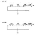
- Figs. 29A and 29B show schematic cross-sectional views that respectively indicate modified examples of the protrusion having a spherical shape.
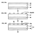
- Figs. 30A, 30B and 30C show cross-sectional views that explain a method for forming the protrusion having the structure shown in Fig. 29B.
- Figs. 31A, 31B and 31C show cross-sectional views that explain a method for forming a protrusion having a structure similar to the structure shown in Fig. 29B.
- Fig. 32 shows a side view that indicates an electrostatic actuator having another structure in accordance with the present invention.
- Fig. 33 shows a side view that indicates an electrostatic actuator having still another structure in accordance with the present invention.
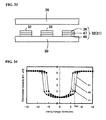
- Fig. 34 shows a drawing that indicates a change in the CV characteristic before and after a thermal endurance test carried out on an electrostatic actuator having protrusions on an insulating film.
- Fig. 35 shows a drawing that explains an electrostatic actuator that has been subjected to the test of Fig. 34.
- Fig. 36 shows a schematic cross-sectional view that indicates a structure of an electrostatic actuator relating to still another embodiment of the present invention.
- Fig. 37 shows a schematic cross-sectional view that indicates a structure of an electrostatic actuator relating to still another embodiment of the present invention.
- Fig. 38 shows a schematic cross-sectional view that indicates a structure of an electrostatic actuator relating to still another embodiment of the present invention.
- Fig. 39 shows a schematic cross-sectional view that indicates a structure of an electrostatic actuator relating to still another embodiment of the present invention.
- Fig. 40 shows a schematic cross-sectional view that indicates a structure of an electrostatic actuator relating to still another embodiment of the present invention.
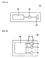
- Fig. 41 shows a schematic drawing that indicates a radio device using an electrostatic micro-relay in accordance with the present invention.
- Fig. 42 shows a schematic drawing that indicates a measuring device using an electrostatic micro-relay in accordance with the present invention.
- Fig. 43 shows a schematic drawing that indicates a temperature-controlling device using an electrostatic micro-relay in accordance with the present invention.
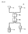
- Fig. 44 shows a schematic drawing that indicates a portable terminal using an electrostatic micro-relay in accordance with the present invention.
- Fig. 7 shows a perspective view of an electrostatic actuator in accordance with one embodiment of the present invention
- Fig. 8 shows a cross-sectional view taken along line X-X
- Fig. 9 shows an exploded perspective view that shows a structure of the electrostatic actuator.
- This electrostatic actuator 21 comprises a micro-machined relay manufactured by using a micro-machining technique, and includes a fixed substrate 22, a movable substrate 23 and a cap 24.
- two signal lines 26, 27 are formed on a substrate 25 (which may be a glass substrate or the like) by using a metal film, and ends of the respective signal lines 26, 27 are aligned face to face with each other with a small gap in between so that respective ends of the signal lines 26, 27 form fixed contacts 28, 29 on the center portion of the upper face of the substrate 25.
- fixed electrodes 30 are placed on both of the right and left sides of each signal line 26, 27, and the fixed electrodes 30 on both of the sides are connected to each other through a gap between the fixed contacts 28, 29.
- the surface of each of the fixed electrodes 30 is coated with an insulating film 31.
- a plurality of fine protrusions 32 are formed on the upper surface of the insulating film 31.
- the size of the protrusions 32 is set to several 0,01 ⁇ m (100 angstroms) to several 0,1 ⁇ m (1000 angstroms); however, in Fig. 9, for convenience of explanation, both of the diameter and protrusion height of the protrusion 32 are depicted in an enlarged manner in comparison with the actual relative dimension.
- the movable substrate 23 is made of Si and has conductivity, and movable electrodes 38 are formed on both sides of a movable contact area 35 formed virtually in the center thereof through elastic supporting portions 36, and anchors 42 are formed on the respective movable electrodes 38 through elastic bending portions 40. Moreover, a movable contact 45, made of a conductive material such as metal, is formed on the lower surface of the movable contact area 35 from an insulating layer 44 made of an oxide film (SiO 2 ) and a nitride film (SiN).
- the movable substrate 23 is elastically supported above the fixed substrate 22 by securing the anchor 42 onto the fixed substrate 22 by an anode joining process or the like; thus, the movable electrode 38 is aligned face to face with the fixed electrode 30 through the insulating film 31, with the movable contact 45 facing both of the fixed contacts 28, 29 in a manner so as to bridge over these.
- the movable substrate 23 is secured onto the upper surface of the fixed substrate 22 so that it is electrically connected to the movable electrode pad 34.
- the cap 24 is put on the fixed substrate 22 over the movable substrate 23 that is joined to the upper surface of the fixed substrate 22, and joined to the upper surface of the fixed substrate 22 by using a sealing material such as low-melting-point glass in a manner so as to surround the peripheral portion of the lower surface. Consequently, the movable substrate 23, the fixed contacts 28, 29, the fixed electrode 30, etc. are sealed in the recessed section 46 of the cap 24 in an air-tight manner.
- Fig. 10 shows a structure of the insulating film 31 that is used for preventing short-circuiting between the fixed electrode 30 and the movable electrode 38.
- the insulating film 31 has a multi-layer structure, and comprises an oxide film (SiO 2 ) 48, a nitride film (SiN) 47 and an oxide film (SiO 2 ) 39 placed in this order from the electrode side.
- the film thickness of the oxide film 48 closest to the electrode is preferably made thinner so that the charge quantity due to ions is minimized as small as possible, with the thickness of the nitride film 47 that is hardly chargeable being set to a comparatively great value, so that proper properties such as voltage resistant property are maintained, and the nitride film 47 is covered with the oxide film 39 so that processing properties upon forming the insulating film 31 are properly maintained.
- a driving voltage Vdrive which is higher than an on-voltage, is applied between the fixed electrode 30 and the movable electrode 38 so that an electrostatic force is generated.
- Vdrive which is higher than an on-voltage
- the elastic bending portion 40 of the movable substrate 23 is distorted to allow the movable electrode 38 to shift toward the fixed electrode 30 side.
- the movable contact 45 is first allowed to contact the fixed contacts 28, 29 to close the fixed contacts 28, 29; thus, the two signal lines 26, 27 are electrically conducted to each other.
- the movable contact 45 comes into contact with the fixed contacts 28, 29, the movable electrode 38 is further attracted to the fixed electrode 30, and allowed to adhere to the fixed electrode 30 with the insulating film 31 being interpolated in between.
- the movable contact 45 is made in press-contact with the fixed contacts 28, 29 through an elastic force by the elastic supporting portion 36.
- the driving voltage Vdrive is removed to eliminate the electrostatic force so that the movable electrode 38 is returned to its original shape through an elastic force to be separated from the fixed electrode 30 with the movable contact 45 being substantially simultaneously separated from the fixed contacts 28, 29; thus, the signal lines 26 and 27 are electrically disconnected.
- the fixed contacts 28, 29 are opened, the contact opening force is increased by the elastic force of the elastic supporting portion 36 so that the fixed contacts 28 and 29 are immediately disconnected.
- the fine protrusions 32 are formed on the surface of the insulating film 31 so that, when the electrostatic actuator 21 is driven and the movable electrode 38 is allowed to adhere to the fixed electrode 30 through the insulating film 31, the movable electrode 38 and the insulating film 31 are not allowed to contact each other over the entire faces thereof, but only allowed to contact each other at the protrusions 32.
- the area of the protrusions 32 formed on the insulating film 31 is allowed to change the quantity of positive charge due to the charge transfer as shown in Fig. 11.
- the total area of the protrusions 32 (the number of the protrusions 32 and the individual areas thereof) is adjusted so that the charge quantity between the movable electrode 38 and the insulating film 31 is controlled and the degree of the plus shift is adjusted.
- the charge transfer is reduced by making the contact area between the insulating film 31 and the movable electrode 38 through the protrusions 32 smaller so that it is possible to reduce the occurrence of the charging due to the plus shift.
- the minus shift is caused by a biased state of ions inside the oxide film 48 as described above, it is possible to control the minus shift by adjusting the thickness of the oxide film 48. In particular, it is possible to reduce the charge quantity due to the minus shift by reducing the thickness of the oxide film 48.
- the oxide film 48 (the insulating film 31) is made thinner, the voltage proof between the movable electrode 38 and the fixed electrode 30 is lowered. Therefore, in this electrostatic actuator 21, a layer of a nitride film 47 that hardly transmits ions is formed in the insulating film 31, and as shown in Fig. 12, by making the oxide film 48 thinner in a corresponding manner, the biased states of cations p and anions n are alleviated with the voltage proof property being maintained in the same manner to suppress the minus shift.
- this electrostatic actuator 21 it is possible to control the plus shift and the minus shift, to improve the CV characteristic of the electrostatic actuator 21, and consequently to control the charging phenomenon due to the plus shift and minus shift and the like.
- operational voltage characteristics such as on-voltage and off-voltage, and consequently to reduce variations thereof.
- neither the control of the plus shift by the use of the protrusions 32 nor the control of the minus shift by the use of the thickness of the oxide film 48 intend to reduce the charge quantity of the insulating film 31 due to the plus shift or the charge quantity of the insulating film 31 due to the minus shift.
- the charge quantity due to the plus shift and the charge quantity due to the minus shift are allowed to cancel each other to be set to zero; thus, as a whole, the charge quantity in the insulating film 31 is set to zero.
- the plus shift is determined by using the sum of the contact areas of the protrusions 32 and the movable electrode 38 as a main factor so that the plus shift is controlled by adjusting the number and the contact areas of the protrusions 32, and the minus shift is determined by the total film thickness of the insulating film 31, and in particular, the film thickness of the oxide film 48 closest to the electrode forms a main factor so that the minus shift is controlled by adjusting the film thickness of the oxide film 48. Therefore, the plus shift is controlled by the protrusions 32, the minus shift is adjusted by the thickness of the oxide film 48, and the charge quantity due to the plus shift and the charge quantity due to the minus shift are allowed to cancel each other to set the sum of the two factors to zero.
- the electrical potential difference caused by the charge of the plus shift may be arranged to cancel the electrical potential difference caused by the charge of the minus shift.
- the shift toward the plus side and the shift toward the minus side are set to cancel each other so as to eliminate the shift of the center value of the CV characteristic.
- the insulating film 31 is formed on the fixed electrode 30; however, as shown in Fig. 13, the insulating film 31 may be formed on the movable electrode 38. Moreover, as shown in Fig. 14, the insulating films 31 may be formed on both of the fixed electrode 30 and the movable electrode 38 (for example, the nitride film 47 is formed on the movable electrode 38 with the oxide film 48 being formed on the fixed electrode 30); in this case, the protrusions 32 are formed on either one of them. Moreover, as shown in Fig. 15, the insulating film 31 and the protrusions 32 may be separated, and the insulating film 31 may be formed on one of the fixed electrode 30 and the movable electrode 38, with the protrusions 32 being formed on the other.
- an electrostatic actuator in which only either the plus shift or the minus shift occurs.
- an electrostatic actuator having a contact area of zero for example, the elasticity of the elastic bending portion is too high so that the movable electrode is not allowed to contact the fixed electrode and the insulating film.
- such an electrostatic actuator has problems that it needs to have a greater size, and that it needs a greater electrode size to compensate for the reduction in the driving force (torque) so as to obtain the same driving force, so no plus shift due to the charge transfer occurs.
- the present invention can be widely applied as an electrostatic actuator in which the fixed electrode and the movable electrode are aligned face to face with each other with an insulating film interpolated in between.
- the electrostatic actuators, shown in Figs. 7 to 9, have structures to be applied to electrostatic micro-relays, and in general, the electrostatic actuator of the present invention does not require the fixed contact and the movable contact.
- the explanation will be given by using the same reference numerals as those used in the electrostatic actuators of Figs. 7 to 9, the subject of application is not intended to be limited to an electrostatic actuator shown in Figs. 7 to 9, etc.
- an insulating film 31 is formed on the fixed electrode 30 by stacking an oxide film 48 and a nitride film 47 thereon from the lower surface side. Moreover, in the insulating film 31 shown in Fig. 17, a nitride film 47 and an oxide film 48 are stacked on the fixed electrode 30 from the lower surface side. In the insulating film 31 shown in Fig. 18, a nitride film 47, an oxide film 48 and a nitride film 47 are stacked on the fixed electrode 30 from the lower surface side. Moreover, as shown in Fig.
- an oxide film 48 and a nitride film 47 may be stacked on the fixed electrode 30 in a desired order, and a third insulating film 49 other than the nitride film 47 and the oxide film 48 may be stacked thereon.
- an insulating film constituted by not less than four layers including a nitride film and an oxide film may be used.
- the oxide film and the nitride film are compared with respect to easiness of charging, the oxide film is charged not less than 100 times as easily as the nitride film.
- the contact area between the movable electrode 38 and the fixed electrode 30 is extremely small (for example, when the protrusion has a cone shape as shown in Fig. 27)
- the amount of plus shift becomes smaller.
- the oxide film 48 is easily charged, with the result that, even when this is made thinner, imbalance between the charge quantity due to the plus shift and the charge quantity due to the minus shift tends to occur.
- the nitride film 47 which is hardly charged, is placed closest to the electrode to control the charge quantity.
- the explanation has exemplified a case in which the insulating film 31 is formed on the fixed electrode 30; however, this may of curse be formed on the movable electrode 38.
- the first and second embodiments have exemplified an insulating film constituted by a nitride film and an oxide film; however, the material for the insulating film which is formed on the electrode is not limited to a nitride film and an oxide film.
- the charge quantity in the insulating film 31 is mainly determined by the film thickness of the oxide film 48, with the nitride film 47 being only used for maintaining a film thickness required for a proper voltage proof characteristic or the like; therefore, not limited to the nitride film 47 and the oxide film 48, any kind of material may be used as long as it has these functions.
- the application of a combination of an oxide film (SiO 2 ) and a nitride film (SiN) makes it possible to obtain the effect of controlling the minus shift, to optimize the manufacturing technique, and consequently to easily manufacture an electrostatic actuator with high yield.
- the effect of the former film that is, the controlling function of the minus shift
- the film thickness of the oxide film 48 closest to the electrode side is controlled by controlling the film thickness of the oxide film 48 closest to the electrode side, and the film thickness of the insulating film 48 is made thinner so that it hardly contains ions.
- the characteristic of the latter film, that is, to provide a high yield is obtained by compensating for the property of the nitride film 47, that is, difficulty in processing, by the use of the oxide film 39.
- the nitride film Upon etching, the nitride film has problems with processing in that it has a low selectivity with respect to glass and silicon, and in that no effective wet-etchant is available; therefore, when all the portion of the insulating film 31 is made of a nitride film 47, over-etching occurs on the substrate 25 made of glass and other metal layers, and unnecessary damages are caused, resulting in degradation in the processing precision.
- One of the solutions of these is to provide a structure which makes it possible to prevent the nitride film 47 from directly contacting the glass and other metals; and with respect to such a buffering layer, an oxide film 39, which is easily processed and has necessary dielectric constant and insulating property, is used to coat the surface of the nitride film 47.
- the protrusions 32 may be formed on the same side as the insulating film 31 of the fixed electrode 30 and the movable electrode 38, or may be formed on the opposite side thereof.
- these may be formed integrally with the insulating film 31 or may be formed in a separate manner.
- the protrusions 32 may be formed by the same material as the constituent material of the insulating film 31, that is, for example, an oxide (SiO 2 ) and a nitride (SiN), or may be formed by a material different from the insulating film 31, for example, a metal.
- the protrusions 32 when the protrusions 32 are formed on the side different from the insulating film 31, for example, on the movable electrode 38, the protrusions 32 may be formed on the surface of the electrode (for example, the movable electrode 38) by an electrode material.
- an insulating film 31 is formed on either one of the fixed electrode 30 and the movable electrode 38, and protrusions 32 are formed integrally with the insulating film 31 on the upper surface of the insulating film 31 by using the same material as the insulating film 31 (the uppermost layer).
- protrusions 32 are independently formed on the upper surface of the insulating film 31 by using an insulating material different from the insulating film 31 (the uppermost layer).
- protrusions 32 are formed on the upper surface of the insulating film 31 by using a conductive film.
- an insulating film 31 is formed on either one of the fixed electrode 30 and the movable electrode 38, and protrusions 32 are formed on an opposite face of the other electrode integrally with the corresponding electrode by the same material as the corresponding electrode.
- protrusions 32 are formed on an opposite face of an electrode different from the electrode on which an insulating film 31 has been formed, that is, either one of the fixed electrode 30 and the movable electrode 38, by using an insulating material.
- protrusions 32 are formed on an opposite face of an electrode different from the electrode on which an insulating film 31 has been formed, that is, either one of the fixed electrode 30 and the movable electrode 38, by using a conductive material that is different from the material of the electrode. Additionally, in Figs. 20 to 25, the insulating film 31 is located on the fixed electrode side; however, the insulating film 31 may be located on the movable electrode side, with the fixed electrode 30 and the movable electrode 38 being replaced by each other.
- Fig. 26A shows a cylinder-shaped protrusion 32
- Fig. 27A shows a cone-shaped protrusion 32
- Fig. 28A shows a protrusion 32 whose surface has a spherical shape.
- the space filling rate between the electrodes is high as shown in Fig. 26B; however, this causes a greater contact area to the movable electrode 38, resulting in a reduction in the suppressing effect of the plus shift.
- the contact area to the movable electrode 38 is small as shown in Fig.
- a column-shaped base post 32a is formed on the insulating film 31, and an uncured protrusion material is dropped thereon to form a curved portion 32b having a spherical shape by utilizing surface tension; thus, a protrusion 32 is formed by the base post 32a and the curved portion 32b.
- a column-shaped base post 32a is formed on the insulating film 31, and a protrusion material is deposited on the insulating film 31 over this structure by sputtering or the like to form a curved portion 32b; thus, a protrusion 32 is formed by the base post 32a and the curved portion 32b.
- Figs. 30A, 30B, 30C are cross-sectional views that explain a manufacturing method of the structure shown in Fig. 29B.
- an oxide film 48 is formed on a fixed electrode 30 by a primary sputtering process, a nitride film 47 is formed thereon, and an oxide film 50 is further formed thereon (Fig. 30A).
- the upper oxide film 50 is processed by etching or the like so that a plurality of base posts 32a having a column shape are formed on the nitride film 47 (Fig. 30B).
- Figs. 31A, 31B and 31C are cross-sectional views that explain a manufacturing method of a structure that is similar to the structure shown in Fig. 29B.
- an oxide film 50 is formed on the fixed electrode 30 by a primary sputtering process (Fig. 31A).
- the oxide film 50 is processed by etching, etc. so that a plurality of base posts 32a having a column shape are formed on the fixed electrode 30 (Fig. 31B).
- each curved portion 32b has a virtually spherical shape at a portion of each base post 32a to achieve a structure similar to the structure of Fig. 29B.
- each protrusion 32, formed by each base post 32a and the oxide film (curved portion 32b) on the upper surface thereof as described in Figs. 31A, 31B and 31C, nor the oxide film between the base posts 32a is formed on the insulating film 31 so that each base post 32a and the oxide film itself also have functions as the insulating film 31.
- each protrusion 32 itself forms the insulating film 31.
- the protrusions 32 shown in Fig. 32 are formed on the fixed electrodes 30 by using an insulating material such as an oxide so that each protrusion 32 also serves as the insulating film 31.
- each protrusion 32 shown in Fig. 33 is formed by stacking the oxide film 48, the nitride film 47 and the oxide film 39 on the fixed electrode 30 so that each protrusion 32 is also allowed to serve as the insulating film 31.
- the insulating film 31 and the protrusion 32 are explained in a separate manner, and in the case when the protrusions 32 are formed simultaneously as the nitride film 47 is formed on the insulating film 31, the structures of the insulating film and the structures of the protrusions, as described above (including those not described above), may be desirably combined.
- the insulating film 31 containing the nitride film 47, as described in the second embodiment, and the protrusions 32, as described in the third embodiment may be respectively used in an independent manner.
- the film thickness of the oxide film 48 may be made thinner so as to reduce the minus shift.
- the film thickness of the oxide film 48 is made thinner so as to control only the charge quantity caused by the minus shift, and the charge quantity of the plus shift that is not controlled is cancelled by using the charge quantity due to the controlled minus shift; thus, the charge quantity as a whole is set to zero.
- the film thickness of the insulating film 31 as a whole may be controlled.
- the plus shift may be reduced by forming the protrusion 32.
- the charge quantity due to the plus shift is controlled by the contact area of the protrusion 32 so that the charge quantity of the minus shift that is not controlled is cancelled by using the charge quantity due to the controlled plus shift; thus, the charge quantity as a whole is set to zero.
- Fig. 34 shows a drawing that indicates a change in the CV characteristic before and after the thermal endurance test of an electrostatic actuator so as to confirm the effects of the protrusions 32.
- an insulating film 31 made of an oxide film (SiO 2 ) is formed on the fixed electrode, with the protrusion 32 made of an oxide film (SiO 2 ) being formed on the insulating film 31 in the same manner, so that an electrostatic actuator is formed.
- the thickness T of the insulating film 31 is set to 0,2 to 0,25 ⁇ m (2000 to 2500 angstroms)
- the height H of each protrusion 32 is set to 0,04 to 0,06 ⁇ m (400 to 600 angstroms)
- the diameter D of each protrusion 32 is set to 25 to 35 ⁇ m
- a plurality of protrusions 32 are formed with pitches P set to 100 to 110 ⁇ m.
- those indicated by broken lines and rhomboidal shape points represent an initial CV characteristic F0 of an electrostatic actuator.
- the characteristic F+ indicated by solid lines and square points represents the CV characteristic of the electrostatic actuator having the plus shift
- the characteristic F- indicated by solid lines and triangular points represents the CV characteristic of the electrostatic actuator having the minus shift.
- Figs. 36 and 37 show portions of the fixed electrode 30 and the movable electrode 38 of an electrostatic actuator in accordance with still another embodiment of the present invention.
- at least one electrode of the fixed electrode 30 and the movable electrode 38 is curved so that the contact area of the insulating film 31 and the electrode is made smaller to suppress the plus shift.
- Fig. 36 will be explained.
- an insulating film 31 including a nitride film 47 is formed on a flat fixed electrode 30, and the movable electrode 38 is curved into a groove shape or a spherical shape so as to make the center portion stick toward the fixed electrode 30 side.
- the contact area of the movable electrode 38 and the insulating film 31 is made smaller so that the plus shift is suppressed, and the film thickness of the oxide film 48 is made thinner so that the minus shift is also suppressed.
- the contact area of the movable electrode 38 and the insulating film 31 is made smaller so that the plus shift is suppressed, and the film thickness of the oxide film 48 is made thinner so that the minus shift is also suppressed.
- the fixed electrode 30 is curved into a groove shape or a spherical shape so as to stick toward the movable electrode 38 side, and an insulating film 31 including a nitride film 47 is formed on the fixed electrode 30.
- the fixed electrode 30 and the insulating film 31 are curved, with the result that the contact area of the movable electrode 38 and the insulating film 31 is made smaller so that the plus shift is suppressed, and the film thickness of the oxide film 48 is made thinner so that the minus shift is suppressed.
- the movable electrode 38 may be attracted toward the fixed electrode side, and elastically distorted into a groove shape or a spherical shape.
- the movable electrode 38 which is supported in a cantilever fashion, may be attracted toward the fixed electrode 30 side so that the movable electrode 38 is diagonally tilted so that the movable electrode 38 is made in contact with the fixed electrode 30 or the insulating film 31 with a small contact area.
- Fig. 38 is a cross-sectional view that shows the structure of an electrostatic actuator in still another embodiment of the present invention.
- a plurality of post-shaped or line-shaped fixed electrodes 30 that are separated with intervals from each other are formed on the upper surface of a substrate 25 made of a glass substrate or the like, and an insulating film 31 is formed on the upper surface of the fixed electrodes 30 in a manner so as to cover the entire fixed electrodes 30.
- a plurality of post-shaped or line-shaped protrusions 32 are formed on the lower face of the movable electrode 38 in a manner so as not to face the fixed electrodes 30.
- either of the fixed electrodes 30 and the protrusions 32 may be formed into a lattice shape or a net shape as long as the fixed electrodes 30 and the protrusions 32 are made face to face with each other without overlapping each other.
- an electric field, exerted between the fixed electrode 30 and the movable electrode 38 is only limited to a portion at which the fixed electrode 30 is formed; therefore, the contact portion between the electrodes, that is, a portion at which each protrusion 32 and the insulating film 31 are made in contact with each other is less susceptible to a great electric field. Therefore, this structure makes it possible to reduce the occurrence of charging due to charge transfer, and consequently to reduce the charge quantity of the plus shift due to charge transfer.
- Fig. 39 is a cross-sectional view that shows a structure of an electrostatic actuator in accordance with still another embodiment of the present invention.
- a plurality of post-shaped or line-shaped fixed electrodes 30 that are separated with intervals from each other are formed on the upper surface of a substrate 25 made of a glass substrate or the like, and the upper surface of the substrate 25 is coated with an insulating film 31 in a manner so as to cover the fixed electrodes 30.
- a plurality of post-shaped or line-shaped protrusions 32 are formed on the upper surface of the insulating film 31 in a manner so as not to face the fixed electrodes 30.
- either of the fixed electrodes 30 and the protrusions 32 may be formed into a lattice shape or a net shape as long as the fixed electrodes 30 and the protrusions 32 are made face to face with each other without overlapping each other.
- an electric field, exerted between the fixed electrode 30 and the movable electrode 38 is only limited to a portion at which the fixed electrode 30 is formed; therefore, the contact portion between the electrodes, that is, a portion at which each protrusion 32 and the insulating film 31 are made in contact with each other is less susceptible to a great electric field. Therefore, this structure makes it possible to reduce the occurrence of charging due to charge transfer, and consequently to reduce the charge quantity of the plus shift due to charge transfer.
- the fixed electrodes 30 are formed partially so as not to overlap the protrusions 32; however, the movable electrode 38 may be formed partially so as not to overlap the protrusion 32 (not shown).
- Fig. 40 is a cross-sectional view that shows the structure of an electrostatic actuator in still another embodiment of the present invention.
- this electrostatic actuator two movable portions 52, each having a diaphragm shape, are supported by a frame 51 along the peripheral portion thereof, and movable electrodes 38 are respectively formed on the opposite faces of the two movable portions 52 so that the surface of at least one of the movable electrodes 38 is coated with an insulating film 31.
- This embodiment shows an example of an electrostatic actuator without any fixed electrode.
- protrusions may be formed on the insulating film 31, or may be formed in a manner so as to face the insulating film 31.
- Fig. 41 shows a schematic drawing that indicates a radio device 61 in which an electrostatic micro-relay 62 of the present invention is used.
- the electrostatic micro-relay 62 is connected between an inner circuit 63 and an antenna 64; thus, by carrying out on-off operations on the electrostatic micro-relay 62, the inner circuit 63 is switched between a transmittable or receivable state and an un-transmittable or un-receivable state through the antenna 64.
- Fig. 42 is a schematic drawing that shows a measuring device 65 using an electrostatic micro-relay 62 in accordance with the present invention.
- the electrostatic micro-relay 62 is connected in the middle of each signal line 67 that reaches each measuring subject (not shown) from the inner circuit 66; thus, the electrostatic micro-relays 62 are turned on and off so that the measuring subjects are switched.
- Fig. 43 is a schematic drawing that shows a temperaturecontrolling device (temperature sensor) 68 using an electrostatic micro-relay 62 in accordance with the present invention.
- This temperature controlling device 68 is attached to a device 69 that requires a safety function with respect to the temperature of the power-supply, control device and the like so that it turns on and off the circuit 70 of the subject device 69, while monitoring the temperature of the subject device 69.
- the temperature controlling device 68 measures the temperature of the subject device 69, and when it detects that the device 69 has been operated for one hour at not less than 100°C, the electrostatic micro-relay 62 inside the temperature controlling device 68 forcefully cuts off the circuit 70.
- Fig. 44 is a schematic drawing that shows a portable terminal 71 such as a cellular phone in which an electrostatic micro-relay in accordance with the present invention is used.
- a portable terminal 71 such as a cellular phone in which an electrostatic micro-relay in accordance with the present invention is used.
- two electrostatic micro-relays 62a, 62b are used.
- One electrostatic micro-relay 62a has a function for switching an inner antenna 72 and an outer antenna 73
- the other electrostatic micro-relay 62b has a function for switching signal flows to a power amplifier 74 on the signal transmission circuit side and a low-noise amplifier 75 on the signal receiving circuit side.
- the electrostatic micro-relay of the present invention makes it possible to transmit dc currents as well as high-frequency signals with low loss, and consequently to maintain a stable characteristic for a long time; thus, by applying this to the above-mentioned radio device 61, the measuring device 65 and the like, it becomes possible to transmit signals with high precision for a long time while reducing the load imposed on the amplifier, etc. used in the inner circuit. Moreover, it is possible to miniaturize the device and also to reduce power consumption; thus, the present invention is highly effective in radio devices that are driven by batteries and measuring devices a plurality of which are used.
- the electrostatic actuator of the present invention it is possible to control the quantities of positive and negative charges in the insulating film by utilizing its charge-quantity controlling structure. For example, it is possible to reduce the quantity of positive or negative charge due to charge transfer and the like, or to reduce the quantity of positive or negative charge due to ionic charging and the like.
- the quantities of positive and negative charges to be generated in the above-mentioned insulating film when a voltage is applied between the first and second electrodes are respectively controlled so that the sum of the quantities of charge in the insulating film is desirably controlled; thus, the quantity of positive charge and the quantity of negative charge are mutually cancelled so that the entire charge quantity (total quantity) generated in the insulating film is controlled.
- the electrostatic actuator of the present invention makes it possible to control the charging phenomena such as plus shift and minus shift, and consequently to control the operational voltage characteristics such as on-voltage and off-voltage.
Landscapes
- Micromachines (AREA)
- Waveguide Connection Structure (AREA)
- Waveguide Switches, Polarizers, And Phase Shifters (AREA)
- Seal Device For Vehicle (AREA)
- Vehicle Body Suspensions (AREA)
- Apparatus For Radiation Diagnosis (AREA)
Abstract
Description
- The present invention relates to an electrostatic actuator, an electrostatic micro-relay and other devices using the same.
- Fig. 1 is an exploded perspective view that shows a structure of a conventional electrostatic actuator and Fig. 2 shows a cross-sectional view thereof. This
electrostatic actuator 1, which is disclosed inJapanese Laid-Open Patent Application No. 2000-164104 fixed substrate 2 and amovable substrate 3. Thefixed substrate 2 is made of a glass substrate having afixed electrode 4 and a pair offixed contacts fixed electrode 4 is coated with aninsulating film 7 made from an oxide. Moreover, thefixed contacts connection pads fixed substrate 2 throughrespective wires 8, 9. - The
movable substrate 3 made from an Si substrate is provided with amovable electrode 13 supported by fourelastic beams 12 in the center portion thereof, and amovable contact 15 is placed on the center portion of the lower face of themovable electrode 13 through aninsulating layer 14. Ananchor 16 protrudes from a peripheral portion of the lower face of themovable substrate 3 so that, when themovable substrate 3 is fixed on the upper face of thefixed substrate 2 by theanchor 16, themovable electrode 13 and thefixed electrode 4 are aligned face to face with each other with a space in between; thus, themovable contact 15 is aligned face to face with thefixed contacts fixed contacts - In this arrangement, when a driving voltage, applied between the
fixed electrode 4 and themovable electrode 13, has reached a predetermined voltage value, themovable electrode 13 is attracted toward thefixed electrode 4 side by an electrostatic attracting force that is exerted between thefixed electrode 4 and themovable electrode 13 so that themovable electrode 13 is allowed to adhere to thefixed electrode 4 through theinsulating film 7 with theelastic beam 12 being distorted. In the case when themovable electrode 13 has adhered to thefixed electrode 4, before or after this process, themovable contact 15 is pressed between thefixed contacts fixed contacts movable contact 15 so that a pair ofconnection pads - Patent
US-A-6,162,657 (D1) discloses in relation to figures 12-19 a micromechanical relay, comprising: a mobile electrode (39, 139) and a fixed electrode (180, 190, 280, 380) facing each other. The mobile electrode (39, 139) carries acontact bridge 40. Saidcontact bridge 40 is for establishing an electrical contact between twocontact pads bridge 40 establishes contact betweencontact pads contact bridge 40 aninsulating layer 50 is provided so as to prevent possible contacting between thecontact bridge 40 and the fixed electrode (180, 190, 280, 380). The insulating film (50) is formed on a face of the first electrode (39) at an area where the first electrode (39) and the second electrode (280) are face to face to one another. An object ofUS-A-6,162,657 is to prevent permanent sticking of themobile electrode 39, 139 of the micromechanical relay to the fixed electrode when the micromechanical relay is in operation. In order to achieve this, the adhesive forces between themovable electrode 39, 139, and the fixed electrode, are reduced, by reducing the contact surface between the two electrodes. The reduction of the contact surface is achieved through roughing of the fixed electrode as described in relation to figures 12, 13, or by providing the surface of the fixed electrode with depressions and elevations as shown in figures 14-16 or by etching pyramids on said surface of the fixed electrode as shown in figures 17-19. -
European patent application EP-A-0 709 911 (D2) discloses micromechanical microwaves micro-switches. A preferred embodiment is described in relation to figures 4a-4e. Said embodiment comprises: a first electrode 415 made of a metal film coated with a dielectric layer 412. The electrode 415 is in two parts. A second electrode in two parts 405, 406 is disposed face to face with the first electrode 415. The dielectric insulating film 412 is between the first and second electrodes. On a central part between the two parts of electrode 415 a metal plate 414 is disposed on the film 412. Two ends 402, 403 of a transmission lines are facing metal plate 414. When no voltage is applied between control electrodes 415 and 405, 406, the metal plate 414 is far from ends 402, 403 of the transmission line. The value of a capacity formed by metal plate 414 coated with dielectric 412 and ends 402, 403 is large. Impedance of said capacity for microwave is large, there is no connection between ends 402, 403 of the transmission line. When a voltage is applied between control electrodes 415 and 405, 406, electrode 415 is attracted toward electrodes 405, 406. The metal plate 414 coated with dielectric film 412 gets near ends 402, 403 of the transmission line. The value of a capacity formed by metal plate 414 coated with dielectric 412 and ends 402, 403 becomes small. Impedance of said capacity for microwave is small enough to be negligible, there is connection, capacitive coupling, between ends 402, 403 of the transmission line. It is indicated that a leaky dielectric 412 should be used to avoid static charge build up in said dielectric, which would act as an activation charge. It is also indicated that the thickness of membrane 412 and metal film 415 provide a tradeoff of the electrode threshold voltage required to pull down and the restoring force required for pull up. -
US-6,307,452 (D3) discloses in relation with figures 5 and 6 a microelectromechanical switch 10 built on asubstrate 12. The switch comprises top andbottom control electrode gap 21 by means of foursprings 22. The micro platform 20 is composed of two bimorph layers including an electrical insulation layer and an electrically conductive film. The dielectric insulation layer acts as a main mechanical structure material while the conductive material acts as the electrostaticcontrol top electrodes 16. Anelectrical contact 32 is formed on a signal line 18. Thecontact 32 is positioned on the signal line to face a shortingbar 34 of the micro platform 20. In operation,switch 10 is normally in a "off" position. When theswitch 10 is in the "off" position, the signal line 18 is an open circuit due togap 21 and the separation of the signal lines 18. Theswitch 10 is actuated to an "on" position by applying a voltage to thetop electrode 16. With a voltage ontop electrode 16, electrostatic forces attract the platform 20 toward thebottom electrode 14 causing theshorting bar 34 with thecontact post 32 to thereby close thegap 21 and place the signal line 18 in the "on" state. Optionally,landing bumpers 26 are positioned beneath each of the foursprings 22 near the micro platform 20. Thebumpers 26 are symmetrically positioned directly beneath the springs at near the point where each spring is connected to the corner of the micro platform 20. In operation, the landing bumpers support the micro platform 20 when the micro platform 20 is moved to an "on" state such that a relatively small area of contact is made between the micro platform 20 and thebottom electrode 14. Stiction problems due to the physical contact between the micro platform 20 and thebottom electrode 14 is dramatically reduced. Then the micro platform 20 is moved to the "on" position, mechanical impact against thesubstrate 12 occurs so that thelanding bumpers 26 which are positioned outside thebottom electrode 14 functional area are used as mechanical buffers to prevent the micro platform 20 from directly impacting against thebottom electrode 14. Thelanding bumpers 26 further reduce the stiction from the charge injection into the dielectric layer of the platform. - Patent
US-A-5 367 429 D4 discloses an electrostatic type micro transducer such as a micro sensor and micro actuator comprisingcontrol electrodes US-A-5 367 429 is to provide an electrostatic type micro transducer having means, which prevents sticking between a movable electrode and a stationary electrode, which may render the electrostatic type micro transducer inoperable. In an embodiment of the invention of D4 described in relation to FIG. 14 a horizontal protrusion 7a is provided forrespective insulator films 7 located at the top end on themovable control electrode 5. The respective horizontal protrusions 7a are adapted to contact initially to one ofstationary control electrodes 6 to thereby prevent the contacting between themovable electrode 5 and one of thestationary electrodes 6. Since the top end of themovable electrode 5 is formed in a taper shape via inclined surfaces 5a, the distance between the possible contacting portion of a horizontal protrusion 7a on thestationary electrode 6 and themovable electrode 5, in that the inclined surface 5a increases, thereby the electrical field strength near theinsulating films 7 is reduced when themovable electrode 5 contacts to one of thestationary electrodes 6 via theinsulator films 7. Accordingly, after the electric field is removed residual dielectric polarization and residual electric charges in theinsulator films 7 are sufficiently reduced and the sticking between the electrodes is eliminated. - In the case of an optimal electrostatic actuator, its CV characteristic is indicated by Fig. 3. Here, the CV characteristic of the electrostatic actuator is represented by the relationship between a driving voltage Vdrive applied between the
fixed electrode 4 and themovable electrode 13 and a capacitance C between the twoelectrodes movable electrode 13 and thefixed electrode 4, C2 represents a value of the capacitance C in a state where themovable electrode 13 adheres to thefixed electrode 4 through theinsulating film 7, on-voltage Von is a value of the driving voltage Vdrive at the time when themovable electrode 13 is made to adhere to the fixed electrode 4 (or is released from the fixed electrode 4), and in the case of an optimal electrostatic actuator, this CV characteristic has a symmetrical profile with respect to the point of the driving voltage Vdrive = 0 volt. - In the case of a conventional electrostatic actuator, for example, the above-mentioned electrostatic actuator, when a driving voltage has been applied between the movable electrode and the fixed electrode for a long time, the insulating film on the fixed electrode is gradually charged, with the result that a variation occurs in operational voltage characteristics, such as on-voltage and off-voltage in the electrostatic actuator. Such a variation in the operational voltage characteristics is caused by the generation of an electrical potential difference other than the driving voltage Vdrive that is externally applied between the fixed electrode and the movable electrode for charging; therefore, when such a variation occurs in the operational voltage characteristics in the electrostatic actuator, the resulting problems are that the electrostatic actuator is not operated even when a rated on-voltage is applied thereto, and that the electrostatic actuator is not turned off even when the applied voltage is turned off. The following description will discuss the causes of variations in the operational voltage characteristics in detail.
- The ways of charging are classified into two ways. Here, these ways are respectively referred to as a plus shift and a minus shift. The plus shift refers to a charging in which the center value of the CV characteristic is shifted toward the plus side of the driving voltage (see Fig. 6). The cause of the plus shift is that a charge transfer (transfer of charge) occurs at a portion on which the insulating film on the fixed electrode and the movable electrode come into contact with each other with the result that the insulating film is charged. The charge transfer is a phenomenon in which, when the contact portion of an insulator and a conductor is subjected to an electric field and heat, a charge is accumulated in the insulator, thereby charging the insulator.
- For example, as shown in Fig. 4, in the case when a driving voltage Vdrive is applied between the
movable electrode 13 and the fixedelectrode 4, with themovable electrode 13 having a positive electric potential, at the contact portion between themovable electrode 13 and the insulatingfilm 7, electrons e on the surface of the insulatingfilm 7 are shifted toward themovable electrode 13 with holes h being left in the insulatingfilm 7 so that the insulatingfilm 7 is positively charged. However, in the case when the polarity of a driving voltage to be applied between the movable electrode and the fixed electrode is reversed so that the movable electrode has a negative electrical potential, the insulating film is negatively charged. - In the event of such a plus shift, the applied voltage Vapp between the
movable electrode 13 and the fixedelectrode 4 is lowered by a voltage ΔVp (>0) corresponding to the charge quantity due to the plus shift charging to a level represented by the following equation:
with the result that the apparent on-voltage is raised to Von + ΔVp (here, Von is a value of the on-voltage in the case of no charge). Therefore, the problem with the plus shift is exerted as an increase in the minimum driving voltage (apparent on-voltage) to be used for closing the fixedcontacts movable contact 15, and in the case of a great plus shift, the electrostatic actuator fails to turn on even when the rated voltage is applied. - Moreover, the minus shift refers to a charging in which the center value of the CV characteristic is shifted toward the minus side of the driving voltage (see Fig. 6). The minus shift is caused by an ionic charging. In other words, this is caused by the fact that ions, generated in processes such as an anodic bonding, are diffused in the insulating film of the oxide so that positive and negative ions diffused in the insulating film are shifted by an electric field applied between the movable electrode and the fixed electrode toward the mutually opposite sides.
- For example, as shown in Fig. 5, in the case when a driving voltage Vdrive is applied between the
movable electrode 13 and the fixedelectrode 4, with themovable electrode 13 having a positive electric potential, anions p, diffused in the insulatingfilm 7 of the oxide, are shifted in the direction toward the interface to the fixedelectrode 4 with anions n being shifted in the direction of the surface of the insulatingfilm 7 so that the surface of the insulatingfilm 7 is negatively charged. However, in the case when the polarity of a driving voltage to be applied between the movable electrode and the fixed electrode is reversed so that the movable electrode has a negative electrical potential, the insulating film is positively charged. - In the event of such a minus shift, the applied voltage Vapp between the
movable electrode 13 and the fixedelectrode 4 is raised by a voltage ΔVn (>0) corresponding to the charge quantity due to the ionic charging to a level represented by the following equation:
with the result that the apparent on-voltage is lowered to Von - ΔVn (here, Von is a value of the on-voltage in the case of no charge). Therefore, the problem with the minus shift is exerted as a decrease in the minimum driving voltage (apparent on-voltage) to be used for opening the fixed contacts, with the result that, even when the driving voltage Vdrive is set to 0 volt, the electrostatic actuator fails to turn off or hardly turns off (that is, the electrostatic actuator is stuck, or susceptible to sticking). - In this manner, the insulating film is always charged while the electrostatic actuator is being driven, resulting in a failure to ensure the designed performances. Fig. 6 shows a change in the CV characteristic before and after a thermal endurance test carried out on an electrostatic actuator. The CV characteristic F0, indicated by broken lines and rhomboidal shape points in Fig. 6, represents an initial characteristic prior to the conduction of the thermal endurance test, which shows a characteristic that is symmetrical with the driving voltage Vdrive. The CV characteristics F+, F-, indicated by solid lines shown in Fig. 6, represent the CV characteristics after a thermal endurance test carried out under conditions of an ambient temperature of 85°C, a driving voltage of 24 volts and test time of 100 hours; and F+ indicated by solid lines and square points, represent plus shifts, while F-, indicated by solid lines and triangular points, represent minus shifts
- In one aspect, the present invention relates to an electrostatic actuator which is provided with means for controlling charging phenomena such as plus shift and minus shift so that it becomes possible to control operational voltage characteristics such as on-voltage and off-voltage. Moreover, in another aspect, the present invention provides an electrostatic micro-relay using the above-mentioned electrostatic actuator and other devices.
- In one embodiment, an electrostatic actuator of the present invention is provided with: a first electrode and a second electrode that are placed face to face with each other; and an insulating film that is formed on an opposing face of at least one electrode of the two electrodes at an area where the first electrode and the second electrode are made face to face with each other so that at least one of the first electrode and the second electrode is driven by an electrostatic force that is exerted when a voltage is applied between the first electrode and second electrode to allow the first electrode and second electrode to contact each other with the insulating film being interpolated in between, and in this arrangement, at least one of the first electrode and second electrode has a structure for controlling charge quantity.
- In accordance with the present invention, since the charge-quantity controlling structure is provided, it is possible to control the quantities of positive and negative charges in the insulating film. For example, it becomes possible to reduce the quantity of a positive or negative charge caused by, for example, charge transfer and the like, or it becomes possible to reduce the quantity of a positive or negative charge caused by ionic charging and the like. As a result, it is possible to control the operational voltage characteristics such as on-voltage and off-voltage of the electrostatic actuator by controlling the charging phenomena such as plus shift and minus shift.
- Moreover, according to the present invention, the above-mentioned charge-quantity controlling structure has such an arrangement that the quantities of positive and negative charges, exerted when a voltage is applied between the first and second electrodes, are respectively controlled so that the sum of the quantities of charge in the insulating film is controlled. The quantity of positive charge and the quantity of negative charge are mutually cancelled so that the entire charge quantity (total quantity) generated in the insulating film is controlled. In particular, it is not necessary to reduce the quantity of positive charge and the quantity of negative charge, and by making the quantity of positive charge and the quantity of negative charge cancel with each other, it becomes possible to reduce the entire charge quantity generated in the insulating film, and consequently to control the charge quantity to, for example, zero.
- In another aspect of the present invention, the thickness of the insulating film is adjusted so that the charge quantity in the insulating film is controlled. In accordance with this aspect, by adjusting the thickness of the insulating layer (in particular, the thickness of the oxide film), the quantity of positive or negative charge of the insulating film due to, for example, ionic charging can be controlled. Moreover, in the case when the insulating film is constituted by a plurality of layers made of different materials, the charge quantity in the insulating film is preferably controlled based upon the thickness of a layer that is directly made in contact with the first electrode or the second electrode.
- Furthermore, in a preferred aspect, the insulating film comprises an oxide film and a nitride film; thus, another effect for reducing the charge quantity due to ionic charging is obtained, and it becomes possible to optimize the manufacturing processes and consequently to manufacture an electrostatic actuator easily with high yield. In other words, the nitride film has a property of hardly transmitting ions, and since the application of a nitride film makes it possible to reduce the thickness of the oxide film while a proper voltage-resistant property is maintained, it becomes possible to reduce the charge quantity in the insulating film due to the ionic charging. In particular, the film is formed as a silicon oxide film or a silicon nitride film so that it becomes possible to manufacture an electrostatic actuator easily with high yield.
- It is preferable to coat the surface of the above-mentioned nitride film with the above-mentioned oxide film. In particular, the nitride film surface on the side opposite to the electrode fixing the insulating film is preferably covered with the oxide film. When the nitride film is exposed, the nitride film is susceptible to damages upon manufacturing, causing degradation in the processing precision; however, it is possible to prevent damages to the nitride film by coating the nitride film with the oxide film.
- Moreover, the above-mentioned insulating layer may be formed by a single material. The formation of the insulating film using a single material makes it possible to simplify the structure of the insulating film, and consequently to easily manufacture the insulating film.
- In another aspect of the present invention, the first and second electrodes being spaced apart by the insulating film interposed between them, the charge quantity in the insulating film is controlled by adjusting a contact area of the two electrodes through the insulating film, in the area on which the first electrode and the second electrode are aligned face to face with each other. In accordance with this aspect, by adjusting the contact area of the two electrodes with each other through the insulating film, it is possible to control the quantity of positive or negative charge of the insulating film due to, for example, a charge transfer.
- For example, at least one protrusion may be formed on at least one of the surfaces of the electrodes in which the contact with the other electrode is made through the film; thus, it is possible to control the entire contact area of the portion in which the contact through the film are made by using the protrusion (for example, the number and the respective contact areas of the protrusions). The surface of this protrusion is preferably formed into a spherical shape. The formation of the surface of the protrusion into a spherical shape makes it possible to reduce the contact area to the other electrode, and consequently to reduce the charge quantity due to a charge transfer effectively; thus, it is also possible to increase the space filling rate, and to strengthen the electrostatic force between the two electrodes.
- In still another aspect of the present invention, in an area which corresponds to a contact area where the first electrode and the second electrode are made in contact through the insulating film, one portion of one of the first and second electrodes at least is not facing a portion of the other one of the first and second electrodes. In an embodiment the first electrode is formed in a plurality of post- shaped or line shaped fixed electrodes that are separated from each other by intervals. The first electrode is formed in a plurality of post-shaped or line shaped fixed electrodes that are separated from each other by intervals. A plurality of post shaped or line shaped protrusions are formed on the lower face of the movable electrode or on top of an insulating film formed on the first electrode and said protrusions are not facing the fixed electrodes. In accordance with this aspect, because an electric field generated between the two electrodes is not applied to the contact portion, it is possible to reduce the charge quantity due to a charge transfer.
- An electrostatic actuator according to embodiments of the present invention may be applied to an electrostatic micro-relay. With this electrostatic micro-relay, it is possible to transmit dc currents as well as high-frequency signals with low loss, and consequently to maintain a stable characteristic for a long time.
- Furthermore, an electrostatic actuator according to embodiments of the present invention may be applied to various devices; and examples thereof include a radio device in which the electrostatic micro-relay is installed so as to open and close an electric signal between the antenna and the inner circuit, a measuring device in which the electrostatic micro-relay is installed so as to open and close an electric signal between a measuring subject and the inner circuit, and a personal digital assistance in which the electrostatic micro-relay is installed so as to open and close the inner electric signal. In accordance with these devices, it is possible to transmit signals with high precision for a long time while reducing the load imposed on the amplifier, etc. used in the inner circuit. Moreover, it is possible to miniaturize the device and also to reduce power consumption; thus, the present invention is highly effective in radio devices that are driven by batteries and measuring devices a plurality of which are used.
- Fig. 1 shows an exploded perspective view that indicates a structure of a conventional electrostatic actuator.
- Fig. 2 shows a cross-sectional view of the conventional electrostatic actuator.
- Fig. 3 shows a drawing that indicates a CV characteristic of an optimal electrostatic actuator.
- Fig. 4 shows a schematic drawing that explains a state in which a plus-shift charge is generated between a movable electrode and an insulating film.
- Fig. 5 shows a schematic drawing that indicates a state in which a minus-shift charge is generated in an insulating film.
- Fig. 6 shows a drawing that indicates a change in the CV characteristic before and after a thermal endurance test.
- Fig. 7 shows a perspective view of an electrostatic actuator in accordance with one embodiment of the present invention.
- Fig. 8 shows a cross-sectional view taken along line X-X of Fig. 7.
- Fig. 9 shows an exploded perspective view that indicates a structure of the electrostatic actuator of Fig. 7.
- Fig. 10 shows a schematic cross-sectional view that indicates a structure of an insulating film formed on a fixed electrode in the electrostatic actuator of Fig. 7.
- Fig. 11 shows a schematic drawing that indicates a principle, which suppresses the plus shift by forming a protrusion on the insulating film.
- Fig. 12 shows a schematic drawing that indicates a principle which suppresses the minus shift by forming a nitride film in the insulating film.
- Fig. 13 shows a schematic cross-sectional view that indicates an electrostatic actuator having another structure in accordance with the present invention.
- Fig. 14 shows a schematic cross-sectional view that indicates an electrostatic actuator having still another structure in accordance with the present invention.
- Fig. 15 shows a schematic cross-sectional view that indicates an electrostatic actuator having still another structure in accordance with the present invention.
- Fig. 16 shows a schematic cross-sectional view that indicates an electrostatic actuator having still another structure in accordance with the present invention.
- Fig. 17 shows a schematic cross-sectional view that indicates an electrostatic actuator having still another structure in accordance with the present invention.
- Fig. 18 shows a schematic cross-sectional view that indicates an electrostatic actuator having still another structure in accordance with the present invention.
- Fig. 19 shows a schematic cross-sectional view that indicates an electrostatic actuator having still another structure in accordance with the present invention.
- Fig. 20 shows a schematic cross-sectional view that indicates an electrostatic actuator having still another structure in accordance with the present invention.
- Fig. 21 shows a schematic cross-sectional view that indicates an electrostatic actuator having still another structure in accordance with the present invention.
- Fig. 22 shows a schematic cross-sectional view that indicates an electrostatic actuator having still another structure in accordance with the present invention.
- Fig. 23 shows a schematic cross-sectional view that indicates an electrostatic actuator having still another structure in accordance with the present invention.
- Fig. 24 shows a schematic cross-sectional view that indicates an electrostatic actuator having still another structure in accordance with the present invention.
- Fig. 25 shows a schematic cross-sectional view that indicates an electrostatic actuator having still another structure in accordance with the present invention.
- Fig. 26A shows a perspective view that indicates a protrusion having a cylinder shape, and Fig. 26B shows a schematic drawing that explains a state in which the protrusion occupies a space between the insulating film and the movable electrode.
- Fig. 27A shows a perspective view that indicates a protrusion having a cone shape, and Fig. 27B shows a schematic drawing that explains a state in which the protrusion occupies a space between the insulating film and the movable electrode.
- Fig. 28A shows a perspective view that indicates a protrusion having a spherical shape, and Fig. 28B shows a schematic drawing that explains a state in which the protrusion occupies a space between the insulating film and the movable electrode.
- Figs. 29A and 29B show schematic cross-sectional views that respectively indicate modified examples of the protrusion having a spherical shape.
- Figs. 30A, 30B and 30C show cross-sectional views that explain a method for forming the protrusion having the structure shown in Fig. 29B.
- Figs. 31A, 31B and 31C show cross-sectional views that explain a method for forming a protrusion having a structure similar to the structure shown in Fig. 29B.
- Fig. 32 shows a side view that indicates an electrostatic actuator having another structure in accordance with the present invention.
- Fig. 33 shows a side view that indicates an electrostatic actuator having still another structure in accordance with the present invention.
- Fig. 34 shows a drawing that indicates a change in the CV characteristic before and after a thermal endurance test carried out on an electrostatic actuator having protrusions on an insulating film.
- Fig. 35 shows a drawing that explains an electrostatic actuator that has been subjected to the test of Fig. 34.
- Fig. 36 shows a schematic cross-sectional view that indicates a structure of an electrostatic actuator relating to still another embodiment of the present invention.
- Fig. 37 shows a schematic cross-sectional view that indicates a structure of an electrostatic actuator relating to still another embodiment of the present invention.
- Fig. 38 shows a schematic cross-sectional view that indicates a structure of an electrostatic actuator relating to still another embodiment of the present invention.
- Fig. 39 shows a schematic cross-sectional view that indicates a structure of an electrostatic actuator relating to still another embodiment of the present invention.
- Fig. 40 shows a schematic cross-sectional view that indicates a structure of an electrostatic actuator relating to still another embodiment of the present invention.
- Fig. 41 shows a schematic drawing that indicates a radio device using an electrostatic micro-relay in accordance with the present invention.
- Fig. 42 shows a schematic drawing that indicates a measuring device using an electrostatic micro-relay in accordance with the present invention.
- Fig. 43 shows a schematic drawing that indicates a temperature-controlling device using an electrostatic micro-relay in accordance with the present invention.
- Fig. 44 shows a schematic drawing that indicates a portable terminal using an electrostatic micro-relay in accordance with the present invention.
- Fig. 7 shows a perspective view of an electrostatic actuator in accordance with one embodiment of the present invention, Fig. 8 shows a cross-sectional view taken along line X-X and Fig. 9 shows an exploded perspective view that shows a structure of the electrostatic actuator. This
electrostatic actuator 21 comprises a micro-machined relay manufactured by using a micro-machining technique, and includes a fixedsubstrate 22, amovable substrate 23 and acap 24. - In the fixed
substrate 22, twosignal lines respective signal lines contacts substrate 25. Moreover, fixedelectrodes 30 are placed on both of the right and left sides of eachsignal line electrodes 30 on both of the sides are connected to each other through a gap between the fixedcontacts electrodes 30 is coated with an insulatingfilm 31. Moreover, a plurality offine protrusions 32 are formed on the upper surface of the insulatingfilm 31.Fixed electrode pads 33, which are respectively conductive to the fixedelectrodes 30, are formed on both of the right and left sides of the end of eachsignal line movable electrode pad 34 is placed on one of the corner portions of the upper surface of thesubstrate 25. Here, the size of theprotrusions 32 is set to several 0,01 µm (100 angstroms) to several 0,1 µm (1000 angstroms); however, in Fig. 9, for convenience of explanation, both of the diameter and protrusion height of theprotrusion 32 are depicted in an enlarged manner in comparison with the actual relative dimension. - The
movable substrate 23 is made of Si and has conductivity, andmovable electrodes 38 are formed on both sides of amovable contact area 35 formed virtually in the center thereof through elastic supportingportions 36, and anchors 42 are formed on the respectivemovable electrodes 38 throughelastic bending portions 40. Moreover, amovable contact 45, made of a conductive material such as metal, is formed on the lower surface of themovable contact area 35 from an insulatinglayer 44 made of an oxide film (SiO2) and a nitride film (SiN). Themovable substrate 23 is elastically supported above the fixedsubstrate 22 by securing theanchor 42 onto the fixedsubstrate 22 by an anode joining process or the like; thus, themovable electrode 38 is aligned face to face with the fixedelectrode 30 through the insulatingfilm 31, with themovable contact 45 facing both of the fixedcontacts movable substrate 23 is secured onto the upper surface of the fixedsubstrate 22 so that it is electrically connected to themovable electrode pad 34. - The
cap 24, which is made of glass or the like, has a lower surface on which a recessedsection 46 is formed. Thecap 24 is put on the fixedsubstrate 22 over themovable substrate 23 that is joined to the upper surface of the fixedsubstrate 22, and joined to the upper surface of the fixedsubstrate 22 by using a sealing material such as low-melting-point glass in a manner so as to surround the peripheral portion of the lower surface. Consequently, themovable substrate 23, the fixedcontacts electrode 30, etc. are sealed in the recessedsection 46 of thecap 24 in an air-tight manner. - Fig. 10 shows a structure of the insulating
film 31 that is used for preventing short-circuiting between the fixedelectrode 30 and themovable electrode 38. The insulatingfilm 31 has a multi-layer structure, and comprises an oxide film (SiO2) 48, a nitride film (SiN) 47 and an oxide film (SiO2) 39 placed in this order from the electrode side. In this insulatingfilm 31, the film thickness of theoxide film 48 closest to the electrode is preferably made thinner so that the charge quantity due to ions is minimized as small as possible, with the thickness of thenitride film 47 that is hardly chargeable being set to a comparatively great value, so that proper properties such as voltage resistant property are maintained, and thenitride film 47 is covered with theoxide film 39 so that processing properties upon forming the insulatingfilm 31 are properly maintained. - In the
electrostatic actuator 21 having the above-mentioned arrangement, a driving voltage Vdrive, which is higher than an on-voltage, is applied between the fixedelectrode 30 and themovable electrode 38 so that an electrostatic force is generated. When themovable electrode 38 is attracted by the electrostatic force between the two electrodes, theelastic bending portion 40 of themovable substrate 23 is distorted to allow themovable electrode 38 to shift toward the fixedelectrode 30 side. When themovable electrode 38 has shifted toward the fixedelectrode 30 side, themovable contact 45 is first allowed to contact the fixedcontacts contacts signal lines movable contact 45 comes into contact with the fixedcontacts movable electrode 38 is further attracted to the fixedelectrode 30, and allowed to adhere to the fixedelectrode 30 with the insulatingfilm 31 being interpolated in between. With this arrangement, themovable contact 45 is made in press-contact with the fixedcontacts portion 36. Moreover, when the driving voltage Vdrive is removed to eliminate the electrostatic force so that themovable electrode 38 is returned to its original shape through an elastic force to be separated from the fixedelectrode 30 with themovable contact 45 being substantially simultaneously separated from the fixedcontacts signal lines contacts portion 36 so that the fixedcontacts - In this
electrostatic actuator 21, thefine protrusions 32 are formed on the surface of the insulatingfilm 31 so that, when theelectrostatic actuator 21 is driven and themovable electrode 38 is allowed to adhere to the fixedelectrode 30 through the insulatingfilm 31, themovable electrode 38 and the insulatingfilm 31 are not allowed to contact each other over the entire faces thereof, but only allowed to contact each other at theprotrusions 32. As described earlier, since the plus shift is caused by a charge transfer exerted between themovable electrode 38 and the insulatingfilm 31, the area of theprotrusions 32 formed on the insulatingfilm 31 is allowed to change the quantity of positive charge due to the charge transfer as shown in Fig. 11. Therefore, the total area of the protrusions 32 (the number of theprotrusions 32 and the individual areas thereof) is adjusted so that the charge quantity between themovable electrode 38 and the insulatingfilm 31 is controlled and the degree of the plus shift is adjusted. For example, the charge transfer is reduced by making the contact area between the insulatingfilm 31 and themovable electrode 38 through theprotrusions 32 smaller so that it is possible to reduce the occurrence of the charging due to the plus shift. - Since the minus shift is caused by a biased state of ions inside the
oxide film 48 as described above, it is possible to control the minus shift by adjusting the thickness of theoxide film 48. In particular, it is possible to reduce the charge quantity due to the minus shift by reducing the thickness of theoxide film 48. However, when the oxide film 48 (the insulating film 31) is made thinner, the voltage proof between themovable electrode 38 and the fixedelectrode 30 is lowered. Therefore, in thiselectrostatic actuator 21, a layer of anitride film 47 that hardly transmits ions is formed in the insulatingfilm 31, and as shown in Fig. 12, by making theoxide film 48 thinner in a corresponding manner, the biased states of cations p and anions n are alleviated with the voltage proof property being maintained in the same manner to suppress the minus shift. - Therefore, in accordance with this
electrostatic actuator 21, it is possible to control the plus shift and the minus shift, to improve the CV characteristic of theelectrostatic actuator 21, and consequently to control the charging phenomenon due to the plus shift and minus shift and the like. As a result, for example, in the case of an electrostatic relay or the like, it is possible to control operational voltage characteristics such as on-voltage and off-voltage, and consequently to reduce variations thereof. However, neither the control of the plus shift by the use of theprotrusions 32 nor the control of the minus shift by the use of the thickness of theoxide film 48 intend to reduce the charge quantity of the insulatingfilm 31 due to the plus shift or the charge quantity of the insulatingfilm 31 due to the minus shift. In other words, even in the case when neither the charge quantity due to the plus shift nor the charge quantity due to the minus shift is reduced, by controlling at least one of the plus shift and the minus shift, the charge quantity due to the plus shift and the charge quantity due to the minus shift are allowed to cancel each other to be set to zero; thus, as a whole, the charge quantity in the insulatingfilm 31 is set to zero. More specifically, the plus shift is determined by using the sum of the contact areas of theprotrusions 32 and themovable electrode 38 as a main factor so that the plus shift is controlled by adjusting the number and the contact areas of theprotrusions 32, and the minus shift is determined by the total film thickness of the insulatingfilm 31, and in particular, the film thickness of theoxide film 48 closest to the electrode forms a main factor so that the minus shift is controlled by adjusting the film thickness of theoxide film 48. Therefore, the plus shift is controlled by theprotrusions 32, the minus shift is adjusted by the thickness of theoxide film 48, and the charge quantity due to the plus shift and the charge quantity due to the minus shift are allowed to cancel each other to set the sum of the two factors to zero. Alternatively, the electrical potential difference caused by the charge of the plus shift may be arranged to cancel the electrical potential difference caused by the charge of the minus shift. In the case when it is difficult to directly execute these methods, provision may be made so that, in the CV characteristic after the thermal endurance test, the shift toward the plus side and the shift toward the minus side are set to cancel each other so as to eliminate the shift of the center value of the CV characteristic. - In the above-mentioned embodiment, the insulating
film 31 is formed on the fixedelectrode 30; however, as shown in Fig. 13, the insulatingfilm 31 may be formed on themovable electrode 38. Moreover, as shown in Fig. 14, the insulatingfilms 31 may be formed on both of the fixedelectrode 30 and the movable electrode 38 (for example, thenitride film 47 is formed on themovable electrode 38 with theoxide film 48 being formed on the fixed electrode 30); in this case, theprotrusions 32 are formed on either one of them. Moreover, as shown in Fig. 15, the insulatingfilm 31 and theprotrusions 32 may be separated, and the insulatingfilm 31 may be formed on one of the fixedelectrode 30 and themovable electrode 38, with theprotrusions 32 being formed on the other. - Here, depending on designs, it is assumed that there is an electrostatic actuator in which only either the plus shift or the minus shift occurs. For example, in the case of an electrostatic actuator having a contact area of zero (for example, the elasticity of the elastic bending portion is too high so that the movable electrode is not allowed to contact the fixed electrode and the insulating film. However, such an electrostatic actuator has problems that it needs to have a greater size, and that it needs a greater electrode size to compensate for the reduction in the driving force (torque) so as to obtain the same driving force, so no plus shift due to the charge transfer occurs.
- In the case when only one of the shifts occurs, only either one of the charge-quantity control means, that is, either one of the
protrusion 32 of the insulatingfilm 31 and theoxide film 48 of the insulatingfilm 31, may be used correspondingly. Therefore, the following description will discuss the means for controlling the plus shift and the means for controlling the minus shift in a separate manner, and with respect to means for controlling the minus shift, various modes of the insulatingfilm 31 will be first explained. - Additionally, not limited to the electrostatic actuators as shown in Figs. 7 to 9, the present invention can be widely applied as an electrostatic actuator in which the fixed electrode and the movable electrode are aligned face to face with each other with an insulating film interpolated in between. The electrostatic actuators, shown in Figs. 7 to 9, have structures to be applied to electrostatic micro-relays, and in general, the electrostatic actuator of the present invention does not require the fixed contact and the movable contact. Although, in the following explanation, the explanation will be given by using the same reference numerals as those used in the electrostatic actuators of Figs. 7 to 9, the subject of application is not intended to be limited to an electrostatic actuator shown in Figs. 7 to 9, etc.
- In an electrostatic actuator shown in Fig. 16, an insulating
film 31 is formed on the fixedelectrode 30 by stacking anoxide film 48 and anitride film 47 thereon from the lower surface side. Moreover, in the insulatingfilm 31 shown in Fig. 17, anitride film 47 and anoxide film 48 are stacked on the fixedelectrode 30 from the lower surface side. In the insulatingfilm 31 shown in Fig. 18, anitride film 47, anoxide film 48 and anitride film 47 are stacked on the fixedelectrode 30 from the lower surface side. Moreover, as shown in Fig. 19, anoxide film 48 and anitride film 47 may be stacked on the fixedelectrode 30 in a desired order, and a third insulatingfilm 49 other than thenitride film 47 and theoxide film 48 may be stacked thereon. Alternatively, although not shown in the Figure, an insulating film constituted by not less than four layers including a nitride film and an oxide film may be used. - When the oxide film and the nitride film are compared with respect to easiness of charging, the oxide film is charged not less than 100 times as easily as the nitride film. However, in the case when the contact area between the
movable electrode 38 and the fixedelectrode 30 is extremely small (for example, when the protrusion has a cone shape as shown in Fig. 27), the amount of plus shift becomes smaller. When an attempt is made to set the total charge quantity to zero, it is necessary to make the quantity of minus shift smaller, and one of the methods for this is to make theoxide film 48 thinner; however, theoxide film 48 is easily charged, with the result that, even when this is made thinner, imbalance between the charge quantity due to the plus shift and the charge quantity due to the minus shift tends to occur. In such a case, as described in embodiments shown in Figs. 16 to 19, thenitride film 47, which is hardly charged, is placed closest to the electrode to control the charge quantity. - The explanation has exemplified a case in which the insulating
film 31 is formed on the fixedelectrode 30; however, this may of curse be formed on themovable electrode 38. Moreover, the first and second embodiments have exemplified an insulating film constituted by a nitride film and an oxide film; however, the material for the insulating film which is formed on the electrode is not limited to a nitride film and an oxide film. The charge quantity in the insulatingfilm 31 is mainly determined by the film thickness of theoxide film 48, with thenitride film 47 being only used for maintaining a film thickness required for a proper voltage proof characteristic or the like; therefore, not limited to thenitride film 47 and theoxide film 48, any kind of material may be used as long as it has these functions. - However, the application of a combination of an oxide film (SiO2) and a nitride film (SiN) makes it possible to obtain the effect of controlling the minus shift, to optimize the manufacturing technique, and consequently to easily manufacture an electrostatic actuator with high yield. In other words, the effect of the former film, that is, the controlling function of the minus shift, is achieved by controlling the film thickness of the
oxide film 48 closest to the electrode side, and the film thickness of the insulatingfilm 48 is made thinner so that it hardly contains ions. The characteristic of the latter film, that is, to provide a high yield, is obtained by compensating for the property of thenitride film 47, that is, difficulty in processing, by the use of theoxide film 39. Upon etching, the nitride film has problems with processing in that it has a low selectivity with respect to glass and silicon, and in that no effective wet-etchant is available; therefore, when all the portion of the insulatingfilm 31 is made of anitride film 47, over-etching occurs on thesubstrate 25 made of glass and other metal layers, and unnecessary damages are caused, resulting in degradation in the processing precision. One of the solutions of these is to provide a structure which makes it possible to prevent thenitride film 47 from directly contacting the glass and other metals; and with respect to such a buffering layer, anoxide film 39, which is easily processed and has necessary dielectric constant and insulating property, is used to coat the surface of thenitride film 47. - Next, with respect to a means for controlling the plus shift, various modes of the
protrusions 32 will be explained. Theprotrusions 32 may be formed on the same side as the insulatingfilm 31 of the fixedelectrode 30 and themovable electrode 38, or may be formed on the opposite side thereof. Here, in the case when theprotrusions 32 are formed on the same side as the insulatingfilm 31, these may be formed integrally with the insulatingfilm 31 or may be formed in a separate manner. Theprotrusions 32 may be formed by the same material as the constituent material of the insulatingfilm 31, that is, for example, an oxide (SiO2) and a nitride (SiN), or may be formed by a material different from the insulatingfilm 31, for example, a metal. In particular, when theprotrusions 32 are formed on the side different from the insulatingfilm 31, for example, on themovable electrode 38, theprotrusions 32 may be formed on the surface of the electrode (for example, the movable electrode 38) by an electrode material. - More specifically, in an electrostatic actuator shown in Fig. 20, an insulating
film 31 is formed on either one of the fixedelectrode 30 and themovable electrode 38, andprotrusions 32 are formed integrally with the insulatingfilm 31 on the upper surface of the insulatingfilm 31 by using the same material as the insulating film 31 (the uppermost layer). In a structure shown in Fig. 21,protrusions 32 are independently formed on the upper surface of the insulatingfilm 31 by using an insulating material different from the insulating film 31 (the uppermost layer). In a structure shown in Fig. 22,protrusions 32 are formed on the upper surface of the insulatingfilm 31 by using a conductive film. Moreover, in a structure shown in Fig. 23, an insulatingfilm 31 is formed on either one of the fixedelectrode 30 and themovable electrode 38, andprotrusions 32 are formed on an opposite face of the other electrode integrally with the corresponding electrode by the same material as the corresponding electrode. In a structure shown in Fig. 24,protrusions 32 are formed on an opposite face of an electrode different from the electrode on which an insulatingfilm 31 has been formed, that is, either one of the fixedelectrode 30 and themovable electrode 38, by using an insulating material. In a structure shown in Fig. 25,protrusions 32 are formed on an opposite face of an electrode different from the electrode on which an insulatingfilm 31 has been formed, that is, either one of the fixedelectrode 30 and themovable electrode 38, by using a conductive material that is different from the material of the electrode. Additionally, in Figs. 20 to 25, the insulatingfilm 31 is located on the fixed electrode side; however, the insulatingfilm 31 may be located on the movable electrode side, with the fixedelectrode 30 and themovable electrode 38 being replaced by each other. - Next, the following description will discuss the shape of the
protrusions 32. Fig. 26A shows a cylinder-shapedprotrusion 32, Fig. 27A shows a cone-shapedprotrusion 32, and Fig. 28A shows aprotrusion 32 whose surface has a spherical shape. In the case of the cylinder-shapedprotrusion 32 of Fig. 26A, the space filling rate between the electrodes is high as shown in Fig. 26B; however, this causes a greater contact area to themovable electrode 38, resulting in a reduction in the suppressing effect of the plus shift. Moreover, in the case of the cone-shapedprotrusion 32 shown in Fig. 27A, although the contact area to themovable electrode 38 is small as shown in Fig. 27B, the space filling rate between the electrodes becomes lower. The low space filling rate causes degradation in the attracting force of themovable electrode 38 in the electrostatic actuator. In contrast, in the case of theprotrusion 32 whose surface has a spherical face as shown in Fig. 28A, its contact area is a fine area α formed by its apex as shown in Fig. 28B, and the space filling rate between the electrodes is great, thereby forming anoptimal protrusion 32. Moreover, each of structures, shown in Fig. 29A, 29B, is a modified example of theprotrusion 32 having a spherical shape. In other words, in the structure of Fig. 29A, a column-shapedbase post 32a is formed on the insulatingfilm 31, and an uncured protrusion material is dropped thereon to form acurved portion 32b having a spherical shape by utilizing surface tension; thus, aprotrusion 32 is formed by thebase post 32a and thecurved portion 32b. Moreover, in the structure of Fig. 29B, a column-shapedbase post 32a is formed on the insulatingfilm 31, and a protrusion material is deposited on the insulatingfilm 31 over this structure by sputtering or the like to form acurved portion 32b; thus, aprotrusion 32 is formed by thebase post 32a and thecurved portion 32b. These modified examples make it possible to increase the space filling rate. - Figs. 30A, 30B, 30C are cross-sectional views that explain a manufacturing method of the structure shown in Fig. 29B. In this manufacturing method, an
oxide film 48 is formed on a fixedelectrode 30 by a primary sputtering process, anitride film 47 is formed thereon, and anoxide film 50 is further formed thereon (Fig. 30A). Then, theupper oxide film 50 is processed by etching or the like so that a plurality ofbase posts 32a having a column shape are formed on the nitride film 47 (Fig. 30B). Thereafter, an oxide film is deposited on the upper surface of thenitride film 47 over the base posts 32a to formcurved portions 32b; thus, the surface of eachcurved portion 32b becomes close to a spherical shape at eachbase post 32a so that the structure shown in Fig. 29B is achieved. - Moreover, Figs. 31A, 31B and 31C are cross-sectional views that explain a manufacturing method of a structure that is similar to the structure shown in Fig. 29B. In this manufacturing method, an
oxide film 50 is formed on the fixedelectrode 30 by a primary sputtering process (Fig. 31A). Next, theoxide film 50 is processed by etching, etc. so that a plurality ofbase posts 32a having a column shape are formed on the fixed electrode 30 (Fig. 31B). Thereafter, an oxide film is deposited on the upper surface of the fixedelectrode 30 over the base posts 32a by a secondary sputtering process to form acurved portion 32b; thus, the surface of eachcurved portion 32b has a virtually spherical shape at a portion of eachbase post 32a to achieve a structure similar to the structure of Fig. 29B. Neither eachprotrusion 32, formed by eachbase post 32a and the oxide film (curved portion 32b) on the upper surface thereof as described in Figs. 31A, 31B and 31C, nor the oxide film between thebase posts 32a is formed on the insulatingfilm 31 so that eachbase post 32a and the oxide film itself also have functions as the insulatingfilm 31. - In the structures shown in Figs. 32, 33, each
protrusion 32 itself forms the insulatingfilm 31. In other words, theprotrusions 32 shown in Fig. 32 are formed on the fixedelectrodes 30 by using an insulating material such as an oxide so that eachprotrusion 32 also serves as the insulatingfilm 31. Moreover, eachprotrusion 32 shown in Fig. 33 is formed by stacking theoxide film 48, thenitride film 47 and theoxide film 39 on the fixedelectrode 30 so that eachprotrusion 32 is also allowed to serve as the insulatingfilm 31. - In the second and third embodiments, the insulating
film 31 and theprotrusion 32 are explained in a separate manner, and in the case when theprotrusions 32 are formed simultaneously as thenitride film 47 is formed on the insulatingfilm 31, the structures of the insulating film and the structures of the protrusions, as described above (including those not described above), may be desirably combined. - Moreover, the insulating
film 31 containing thenitride film 47, as described in the second embodiment, and theprotrusions 32, as described in the third embodiment, may be respectively used in an independent manner. In other words, in the case of an electrostatic actuator having a structure for preventing the plus shift, the film thickness of theoxide film 48 may be made thinner so as to reduce the minus shift. Moreover, even in the case when the plus shift and the minus shift are caused, the film thickness of theoxide film 48 is made thinner so as to control only the charge quantity caused by the minus shift, and the charge quantity of the plus shift that is not controlled is cancelled by using the charge quantity due to the controlled minus shift; thus, the charge quantity as a whole is set to zero. In this case, by using thenitride film 47 that is hardly charged, the film thickness of the insulatingfilm 31 as a whole may be controlled. In the same manner, in the case of an electrostatic actuator having a structure for preventing the minus shift, the plus shift may be reduced by forming theprotrusion 32. Moreover, even in the case when the plus shift and the minus shift are caused, only the charge quantity due to the plus shift is controlled by the contact area of theprotrusion 32 so that the charge quantity of the minus shift that is not controlled is cancelled by using the charge quantity due to the controlled plus shift; thus, the charge quantity as a whole is set to zero. - Fig. 34 shows a drawing that indicates a change in the CV characteristic before and after the thermal endurance test of an electrostatic actuator so as to confirm the effects of the
protrusions 32. In other words, as shown in Fig. 35, an insulatingfilm 31 made of an oxide film (SiO2) is formed on the fixed electrode, with theprotrusion 32 made of an oxide film (SiO2) being formed on the insulatingfilm 31 in the same manner, so that an electrostatic actuator is formed. Here, the thickness T of the insulatingfilm 31 is set to 0,2 to 0,25 µm (2000 to 2500 angstroms), the height H of eachprotrusion 32 is set to 0,04 to 0,06 µm (400 to 600 angstroms), the diameter D of eachprotrusion 32 is set to 25 to 35 µm, and a plurality ofprotrusions 32 are formed with pitches P set to 100 to 110 µm. With a driving voltage of the rated voltage being applied between the fixed electrode and the movable electrode of the electrostatic actuator that forms this measuring subject, this has been held at 85°C for 1000 hours, and this is then left at a standard state for two hours. The CV characteristic is measured with respect to the electrostatic actuator having been subjected to such a thermal endurance test, and Fig. 34 shows the results of the measurements. - In Fig. 34, those indicated by broken lines and rhomboidal shape points represent an initial CV characteristic F0 of an electrostatic actuator. Moreover, among the CV characteristics indicated by solid lines in Fig. 34, the characteristic F+ indicated by solid lines and square points represents the CV characteristic of the electrostatic actuator having the plus shift, and the characteristic F- indicated by solid lines and triangular points represents the CV characteristic of the electrostatic actuator having the minus shift. When the CV characteristic of Fig. 34 is compared with the CV characteristic shown in Fig. 6, the shift amounts of F+ and F- in the CV characteristic of Fig. 34 become extremely small, thereby clearly indicating the effects of the formation of the protrusions.
- Figs. 36 and 37 show portions of the fixed
electrode 30 and themovable electrode 38 of an electrostatic actuator in accordance with still another embodiment of the present invention. In this embodiment, at least one electrode of the fixedelectrode 30 and themovable electrode 38 is curved so that the contact area of the insulatingfilm 31 and the electrode is made smaller to suppress the plus shift. - First, Fig. 36 will be explained. In this Figure, an insulating
film 31 including anitride film 47 is formed on a flat fixedelectrode 30, and themovable electrode 38 is curved into a groove shape or a spherical shape so as to make the center portion stick toward the fixedelectrode 30 side. In this embodiment, since themovable electrode 38 is curved, the contact area of themovable electrode 38 and the insulatingfilm 31 is made smaller so that the plus shift is suppressed, and the film thickness of theoxide film 48 is made thinner so that the minus shift is also suppressed. In the same manner, in an embodiment shown in Fig. 37, the fixedelectrode 30 is curved into a groove shape or a spherical shape so as to stick toward themovable electrode 38 side, and an insulatingfilm 31 including anitride film 47 is formed on the fixedelectrode 30. In this embodiment, since the fixedelectrode 30 and the insulatingfilm 31 are curved, with the result that the contact area of themovable electrode 38 and the insulatingfilm 31 is made smaller so that the plus shift is suppressed, and the film thickness of theoxide film 48 is made thinner so that the minus shift is suppressed. - Moreover, different from the embodiment of Fig. 36 in which the
movable electrode 38 has been preliminarily curved, for example, themovable electrode 38, supported at both of the ends, may be attracted toward the fixed electrode side, and elastically distorted into a groove shape or a spherical shape. Alternatively, although not shown in the Figures, themovable electrode 38, which is supported in a cantilever fashion, may be attracted toward the fixedelectrode 30 side so that themovable electrode 38 is diagonally tilted so that themovable electrode 38 is made in contact with the fixedelectrode 30 or the insulatingfilm 31 with a small contact area. - Fig. 38 is a cross-sectional view that shows the structure of an electrostatic actuator in still another embodiment of the present invention. In this electrostatic actuator, a plurality of post-shaped or line-shaped fixed
electrodes 30 that are separated with intervals from each other are formed on the upper surface of asubstrate 25 made of a glass substrate or the like, and an insulatingfilm 31 is formed on the upper surface of the fixedelectrodes 30 in a manner so as to cover the entirefixed electrodes 30. Moreover, a plurality of post-shaped or line-shapedprotrusions 32 are formed on the lower face of themovable electrode 38 in a manner so as not to face the fixedelectrodes 30. Here, either of the fixedelectrodes 30 and theprotrusions 32 may be formed into a lattice shape or a net shape as long as the fixedelectrodes 30 and theprotrusions 32 are made face to face with each other without overlapping each other. - In such an embodiment, an electric field, exerted between the fixed
electrode 30 and themovable electrode 38 is only limited to a portion at which the fixedelectrode 30 is formed; therefore, the contact portion between the electrodes, that is, a portion at which eachprotrusion 32 and the insulatingfilm 31 are made in contact with each other is less susceptible to a great electric field. Therefore, this structure makes it possible to reduce the occurrence of charging due to charge transfer, and consequently to reduce the charge quantity of the plus shift due to charge transfer. - Fig. 39 is a cross-sectional view that shows a structure of an electrostatic actuator in accordance with still another embodiment of the present invention. In this electrostatic actuator, a plurality of post-shaped or line-shaped fixed
electrodes 30 that are separated with intervals from each other are formed on the upper surface of asubstrate 25 made of a glass substrate or the like, and the upper surface of thesubstrate 25 is coated with an insulatingfilm 31 in a manner so as to cover the fixedelectrodes 30. Moreover, a plurality of post-shaped or line-shapedprotrusions 32 are formed on the upper surface of the insulatingfilm 31 in a manner so as not to face the fixedelectrodes 30. Here, either of the fixedelectrodes 30 and theprotrusions 32 may be formed into a lattice shape or a net shape as long as the fixedelectrodes 30 and theprotrusions 32 are made face to face with each other without overlapping each other. - In this embodiment also, an electric field, exerted between the fixed
electrode 30 and themovable electrode 38, is only limited to a portion at which the fixedelectrode 30 is formed; therefore, the contact portion between the electrodes, that is, a portion at which eachprotrusion 32 and the insulatingfilm 31 are made in contact with each other is less susceptible to a great electric field. Therefore, this structure makes it possible to reduce the occurrence of charging due to charge transfer, and consequently to reduce the charge quantity of the plus shift due to charge transfer. - Moreover, in the embodiments of Figs. 38 and 39, the fixed
electrodes 30 are formed partially so as not to overlap theprotrusions 32; however, themovable electrode 38 may be formed partially so as not to overlap the protrusion 32 (not shown). - Fig. 40 is a cross-sectional view that shows the structure of an electrostatic actuator in still another embodiment of the present invention. In this electrostatic actuator, two
movable portions 52, each having a diaphragm shape, are supported by aframe 51 along the peripheral portion thereof, andmovable electrodes 38 are respectively formed on the opposite faces of the twomovable portions 52 so that the surface of at least one of themovable electrodes 38 is coated with an insulatingfilm 31. This embodiment shows an example of an electrostatic actuator without any fixed electrode. Here, in this embodiment also, protrusions may be formed on the insulatingfilm 31, or may be formed in a manner so as to face the insulatingfilm 31. - The following description will discuss a device using electrostatic micro-relays having structures shown in Figs. 7 to 9. Fig. 41 shows a schematic drawing that indicates a
radio device 61 in which anelectrostatic micro-relay 62 of the present invention is used. In thisradio device 61, theelectrostatic micro-relay 62 is connected between aninner circuit 63 and anantenna 64; thus, by carrying out on-off operations on theelectrostatic micro-relay 62, theinner circuit 63 is switched between a transmittable or receivable state and an un-transmittable or un-receivable state through theantenna 64. - Fig. 42 is a schematic drawing that shows a measuring
device 65 using anelectrostatic micro-relay 62 in accordance with the present invention. In this measuringdevice 65, theelectrostatic micro-relay 62 is connected in the middle of eachsignal line 67 that reaches each measuring subject (not shown) from theinner circuit 66; thus, theelectrostatic micro-relays 62 are turned on and off so that the measuring subjects are switched. - Fig. 43 is a schematic drawing that shows a temperaturecontrolling device (temperature sensor) 68 using an
electrostatic micro-relay 62 in accordance with the present invention. Thistemperature controlling device 68 is attached to adevice 69 that requires a safety function with respect to the temperature of the power-supply, control device and the like so that it turns on and off thecircuit 70 of thesubject device 69, while monitoring the temperature of thesubject device 69. For example, supposing that the limit of use of thesubject device 69 is one hour at not less than 100°C, thetemperature controlling device 68 measures the temperature of thesubject device 69, and when it detects that thedevice 69 has been operated for one hour at not less than 100°C, theelectrostatic micro-relay 62 inside thetemperature controlling device 68 forcefully cuts off thecircuit 70. - Fig. 44 is a schematic drawing that shows a
portable terminal 71 such as a cellular phone in which an electrostatic micro-relay in accordance with the present invention is used. In thisportable terminal 71, twoelectrostatic micro-relays electrostatic micro-relay 62a has a function for switching aninner antenna 72 and anouter antenna 73, and the other electrostatic micro-relay 62b has a function for switching signal flows to apower amplifier 74 on the signal transmission circuit side and a low-noise amplifier 75 on the signal receiving circuit side. - The electrostatic micro-relay of the present invention makes it possible to transmit dc currents as well as high-frequency signals with low loss, and consequently to maintain a stable characteristic for a long time; thus, by applying this to the above-mentioned
radio device 61, the measuringdevice 65 and the like, it becomes possible to transmit signals with high precision for a long time while reducing the load imposed on the amplifier, etc. used in the inner circuit. Moreover, it is possible to miniaturize the device and also to reduce power consumption; thus, the present invention is highly effective in radio devices that are driven by batteries and measuring devices a plurality of which are used. - In the case of a low-electric-potential driving device, a dissociation occurs between an applied voltage and a driving voltage due to a charge accumulated in the insulating film, with the result that the applied voltage between the movable electrode and the fixed electrode is not made coincident with the driving voltage Vdrive that is externally applied. Normally, the phenomenon of this type is only recognized as a failure in an electrostatic actuator; however, the present invention makes it possible to utilize this phenomenon as an advantage of the electrostatic actuator. For the first example, there is a case in which an electrostatic relay to be driven by 10 volts is assembled in a circuit in which only an application voltage of three volts is prepared. Even in this case, by designing the circuit so as to accumulate an electric potential of + 7 volts between the movable electrode and the fixed electrode by charging through the charge controlling technique, it becomes possible to obtain an application voltage of 10 volts even in the case of the driving voltage of 3 volts; thus, it is possible to operate the electrostatic relay without causing any problems even in this case. In contrast, in the case when an electrostatic relay to be driven by 3 volts is assembled in a substrate which is designed to be driven by an applied voltage of 10 volts, by designing the charge controlling operation so as to accumulate an electric potential of -7 volts between the movable electrode and the fixed electrode by charging, it is possible to provide a apparent substrate that is equivalently controlled by an electrostatic relay to be driven by 10 volts. These ways of use may be applied not only to an electrostatic relay but also to a switch, an electrostatic capacitive sensor and the like.
- In accordance with the electrostatic actuator of the present invention, it is possible to control the quantities of positive and negative charges in the insulating film by utilizing its charge-quantity controlling structure. For example, it is possible to reduce the quantity of positive or negative charge due to charge transfer and the like, or to reduce the quantity of positive or negative charge due to ionic charging and the like.
- Moreover, the quantities of positive and negative charges to be generated in the above-mentioned insulating film when a voltage is applied between the first and second electrodes are respectively controlled so that the sum of the quantities of charge in the insulating film is desirably controlled; thus, the quantity of positive charge and the quantity of negative charge are mutually cancelled so that the entire charge quantity (total quantity) generated in the insulating film is controlled. In particular, it is not necessary to reduce the quantity of positive charge and the quantity of negative charge, and by making the quantity of positive charge and the quantity of negative charge cancel with each other, it becomes possible to reduce the entire charge quantity generated in the insulating film, and consequently to control the charge quantity as a whole to, for example, zero.
- As a result, the electrostatic actuator of the present invention makes it possible to control the charging phenomena such as plus shift and minus shift, and consequently to control the operational voltage characteristics such as on-voltage and off-voltage.
Claims (23)
- An electrostatic actuator (21), comprising:a first electrode (30) and a second electrode (38) disposed face to face with each other; andan insulating film (31) formed on an opposing face of at least one electrode of the two electrodes (30, 38) at an area where the first electrode (30) and the second electrode (38) are made face to face with each other so that at least one of the first electrode (30) and the second electrode (38) is driven by an electrostatic force that is exerted when a voltage is applied between the first electrode (30) and the second electrode (38) to allow the first electrode (30) and the second electrode (38) to contact each other with the insulating film (31) being interpolated in between, whereinat least one of the first electrode (30) and the second electrode (38) has a structure for controlling charge quantity, characterized in that: said structure for controlling charge quantity is adapted such that the quantities of positive and negative charges, exerted when a voltage is applied between the first and second electrodes (30, 38), are respectively controlled so that the sum of the quantities of charge in the insulating film (31) is controlled.
- The electrostatic actuator (21) according to claim 1, wherein
the thickness of the insulating film (31) is selected such that the charge quantity in the insulating film (31) is controlled. - The electrostatic actuator (21) according to claim 2, wherein
the insulating film (31) comprises a plurality of layers made of different materials, and wherein the charge quantity in the insulating film (31) is controlled based upon the thickness of a layer that is in direct contact with at least one of the first electrode (30) and the second electrode (38). - The electrostatic actuator (21) according to claim 2, wherein
the insulating film (31) comprises an oxide film (39) and a nitride film (47). - The electrostatic actuator (21) according to claim 4, wherein
the nitride film (47) has a surface coated with the oxide film (39). - The electrostatic actuator (21) according to claim 2, wherein
the insulating layer (44) is a single material. - The electrostatic actuator (21) according to claim 1, wherein
the charge quantity in the insulating film (31) is controlled by adjusting a contact area of a portion in which the first electrode (30) and the second electrode (38) are contacting each other through the insulating film (31). - The electrostatic actuator (21) according to claim 1, wherein the insulating film is formed on one of the first and second electrodes (30, 38).
- The electrostatic actuator (21) according to claim 1, wherein the insulating film (31) is formed partly on one of the electrode and partly on the other one of the electrodes.
- The electrostatic actuator (21) according to claim 7, wherein
at least one protrusion (32) is formed on at least one of the surfaces of the portion in which contact and separation of the first electrode (30) and the second electrode (38) are made, so that the contact area of the contact and separation portion is controlled by at least one protrusion (32). - The electrostatic actuator (21) according to claim 8, wherein
the protrusion (32) has a surface formed into a spherical shape. - The electrostatic actuator (21) according to claim 1, wherein
in a contact area where the first electrode (30) and the second electrode (38) are made in contact through the insulating film (31) at least one portion of one of the first and second electrodes is not facing a portion of the other one of the first and second electrodes. - The electrostatic actuator (21) according to claim 10, wherein the first electrode (30) is formed in a plurality of post- shaped or line shaped fixed electrodes (30) that are separated from each other by intervals and a plurality of post shaped or line shaped protrusions (32) are formed on the lower face of the movable electrode (38) or on top of an insulating film (31) formed on the first electrode and said protrusions (32) are not facing said fixed electrodes (30).
- The electrostatic actuator (21) according to claim 7, wherein a plurality of protrusions (32) are formed on the upper surface of the insulating film (31).
- The electrostatic actuator (21) according to claim 14, wherein the protrusions (32) have a cone shape.
- The electrostatic actuator (21) according to claim 14, wherein the protrusions (32) have surfaces that are spherical shaped.
- The electrostatic actuator (21) according to claim 14, wherein the protrusions (32) have a cylinder shape.
- The electrostatic actuator (21) according to one of claims 14-16, wherein a thickness T of the film insulating ranges from 0,2 to 0,25 µm, the height H of the protrusions (32) on top of the insulating film ranging from 0,04 to 0,06 µm and a pitch of the plurality of protrusions (32) ranging from 100 to 110 µm.
- The electrostatic actuator (21) according to claim 17, wherein the diameter of the protrusions (32) ranges from 25 to 35 µm.
- An electrostatic micro-relay (62) comprising the electrostatic actuator according to one of claims 1 to 19, wherein
fixed contacts (28, 29) and a movable contact (45) are made in contact with and separated from each other by utilizing said electrostatic actuator (21). - A radio device (61) comprising the electrostatic micro-relay according to claim 20, wherein
the electrostatic micro-relay (62) is installed so as to open and close an electric signal between an antenna (64) and an inner circuit (63, 66). - A measuring device (65) comprising the electrostatic micro-relay according to claim 20, wherein
the electrostatic micro-relay (62) is installed so as to open and close an electric signal between a measuring subject and an inner circuit (66). - A personal digital assistance comprising the electrostatic micro-relay according to claim 20, wherein
the electrostatic micro-relay (62) is placed so as to open and close an electric signal inside thereof.
Applications Claiming Priority (2)
| Application Number | Priority Date | Filing Date | Title |
|---|---|---|---|
| JP2001340293 | 2001-11-06 | ||
| JP2001340293A JP4045090B2 (en) | 2001-11-06 | 2001-11-06 | Adjustment method of electrostatic actuator |
Publications (3)
| Publication Number | Publication Date |
|---|---|
| EP1308977A2 EP1308977A2 (en) | 2003-05-07 |
| EP1308977A3 EP1308977A3 (en) | 2005-01-19 |
| EP1308977B1 true EP1308977B1 (en) | 2007-08-29 |
Family
ID=19154516
Family Applications (1)
| Application Number | Title | Priority Date | Filing Date |
|---|---|---|---|
| EP02102543A Expired - Lifetime EP1308977B1 (en) | 2001-11-06 | 2002-11-06 | Electrostatic actuator, and electrostatic microrelay and other devices using the same |
Country Status (7)
| Country | Link |
|---|---|
| US (1) | US7161273B2 (en) |
| EP (1) | EP1308977B1 (en) |
| JP (1) | JP4045090B2 (en) |
| KR (1) | KR100499823B1 (en) |
| CN (1) | CN1258795C (en) |
| AT (1) | ATE371947T1 (en) |
| DE (1) | DE60222075T2 (en) |
Families Citing this family (48)
| Publication number | Priority date | Publication date | Assignee | Title |
|---|---|---|---|---|
| US6850133B2 (en) | 2002-08-14 | 2005-02-01 | Intel Corporation | Electrode configuration in a MEMS switch |
| WO2004102744A1 (en) * | 2003-05-14 | 2004-11-25 | Koninklijke Philips Electronics N.V. | Improvements in or relating to wireless terminals |
| FR2868591B1 (en) * | 2004-04-06 | 2006-06-09 | Commissariat Energie Atomique | MICROCOMMUTER WITH LOW ACTUATION VOLTAGE AND LOW CONSUMPTION |
| KR101313117B1 (en) | 2004-07-29 | 2013-09-30 | 퀄컴 엠이엠에스 테크놀로지스, 인크. | System and method for micro-electromechanical operating of an interferometric modulator |
| US7373026B2 (en) | 2004-09-27 | 2008-05-13 | Idc, Llc | MEMS device fabricated on a pre-patterned substrate |
| US7327510B2 (en) * | 2004-09-27 | 2008-02-05 | Idc, Llc | Process for modifying offset voltage characteristics of an interferometric modulator |
| US7369296B2 (en) | 2004-09-27 | 2008-05-06 | Idc, Llc | Device and method for modifying actuation voltage thresholds of a deformable membrane in an interferometric modulator |
| JP4540443B2 (en) * | 2004-10-21 | 2010-09-08 | 富士通コンポーネント株式会社 | Electrostatic relay |
| JP2006210843A (en) * | 2005-01-31 | 2006-08-10 | Fujitsu Ltd | Variable capacitor and manufacturing method thereof |
| JP4506529B2 (en) | 2005-03-18 | 2010-07-21 | オムロン株式会社 | Electrostatic microswitch and method for manufacturing the same, and apparatus provided with electrostatic microswitch |
| JP4008453B2 (en) * | 2005-04-13 | 2007-11-14 | ファナック株式会社 | Electrostatic motor electrode manufacturing method, electrostatic motor electrode and electrostatic motor |
| JP4507965B2 (en) * | 2005-04-15 | 2010-07-21 | セイコーエプソン株式会社 | Method for manufacturing droplet discharge head |
| EP2495212A3 (en) * | 2005-07-22 | 2012-10-31 | QUALCOMM MEMS Technologies, Inc. | Mems devices having support structures and methods of fabricating the same |
| FR2889371A1 (en) * | 2005-07-29 | 2007-02-02 | Commissariat Energie Atomique | DEVICE FOR CONVERTING MECHANICAL ENERGY IN ELECTRIC ENERGY BY CYCLE OF ELECTRICAL LOADS AND DISCHARGES ON THE CONNECTORS OF A CAPACITOR |
| US20070040637A1 (en) * | 2005-08-19 | 2007-02-22 | Yee Ian Y K | Microelectromechanical switches having mechanically active components which are electrically isolated from components of the switch used for the transmission of signals |
| EP1928780A2 (en) | 2005-09-30 | 2008-06-11 | Qualcomm Mems Technologies, Inc. | Mems device and interconnects for same |
| US7652814B2 (en) | 2006-01-27 | 2010-01-26 | Qualcomm Mems Technologies, Inc. | MEMS device with integrated optical element |
| US7751173B2 (en) * | 2006-02-09 | 2010-07-06 | Kabushiki Kaisha Toshiba | Semiconductor integrated circuit including circuit for driving electrostatic actuator, micro-electro-mechanical systems, and driving method of electrostatic actuator |
| US7547568B2 (en) | 2006-02-22 | 2009-06-16 | Qualcomm Mems Technologies, Inc. | Electrical conditioning of MEMS device and insulating layer thereof |
| US7450295B2 (en) | 2006-03-02 | 2008-11-11 | Qualcomm Mems Technologies, Inc. | Methods for producing MEMS with protective coatings using multi-component sacrificial layers |
| US7643203B2 (en) * | 2006-04-10 | 2010-01-05 | Qualcomm Mems Technologies, Inc. | Interferometric optical display system with broadband characteristics |
| US7417784B2 (en) | 2006-04-19 | 2008-08-26 | Qualcomm Mems Technologies, Inc. | Microelectromechanical device and method utilizing a porous surface |
| US7369292B2 (en) * | 2006-05-03 | 2008-05-06 | Qualcomm Mems Technologies, Inc. | Electrode and interconnect materials for MEMS devices |
| US7566664B2 (en) | 2006-08-02 | 2009-07-28 | Qualcomm Mems Technologies, Inc. | Selective etching of MEMS using gaseous halides and reactive co-etchants |
| US7706042B2 (en) * | 2006-12-20 | 2010-04-27 | Qualcomm Mems Technologies, Inc. | MEMS device and interconnects for same |
| US7535621B2 (en) | 2006-12-27 | 2009-05-19 | Qualcomm Mems Technologies, Inc. | Aluminum fluoride films for microelectromechanical system applications |
| JP4611323B2 (en) | 2007-01-26 | 2011-01-12 | 富士通株式会社 | Variable capacitor |
| JP2008204768A (en) * | 2007-02-20 | 2008-09-04 | Omron Corp | Micro relay, wireless communication device, measuring instrument, portable information terminal |
| US7733552B2 (en) | 2007-03-21 | 2010-06-08 | Qualcomm Mems Technologies, Inc | MEMS cavity-coating layers and methods |
| US7719752B2 (en) | 2007-05-11 | 2010-05-18 | Qualcomm Mems Technologies, Inc. | MEMS structures, methods of fabricating MEMS components on separate substrates and assembly of same |
| US8115577B2 (en) * | 2007-06-14 | 2012-02-14 | Panasonic Corporation | Electromechanical switch, filter using the same, and communication apparatus |
| US7570415B2 (en) | 2007-08-07 | 2009-08-04 | Qualcomm Mems Technologies, Inc. | MEMS device and interconnects for same |
| JP5240203B2 (en) * | 2007-10-31 | 2013-07-17 | 富士通株式会社 | Micro movable element and micro movable element array |
| JP5628178B2 (en) * | 2008-09-16 | 2014-11-19 | コーニンクレッカ フィリップス エヌ ヴェ | Capacitive micromachined ultrasonic transducer |
| GB2467777B (en) * | 2009-02-13 | 2011-01-12 | Wolfson Microelectronics Plc | MEMS device and process |
| US8847087B2 (en) | 2009-09-17 | 2014-09-30 | Panasonic Corporation | MEMS switch and communication device using the same |
| WO2011033728A1 (en) * | 2009-09-17 | 2011-03-24 | パナソニック株式会社 | Mems switch and communication device using the same |
| JP5338615B2 (en) | 2009-10-27 | 2013-11-13 | 富士通株式会社 | Variable capacitance device and method of driving variable capacitance element |
| JP5402823B2 (en) * | 2010-05-13 | 2014-01-29 | オムロン株式会社 | Acoustic sensor |
| JP5609271B2 (en) | 2010-05-28 | 2014-10-22 | 大日本印刷株式会社 | Electrostatic actuator |
| CN102044380A (en) * | 2010-12-31 | 2011-05-04 | 航天时代电子技术股份有限公司 | Metal MEMS (micro-electromechanical system) electromagnetic relay |
| JP6165730B2 (en) * | 2011-09-02 | 2017-07-19 | キャベンディッシュ・キネティックス・インコーポレイテッドCavendish Kinetics, Inc. | MEMS device anchoring |
| JP2013090442A (en) * | 2011-10-18 | 2013-05-13 | Murata Mfg Co Ltd | Electrostatic drive type actuator, variable capacitance element and method of manufacturing the same |
| US8629360B2 (en) * | 2012-04-30 | 2014-01-14 | Raytheon Company | RF micro-electro-mechanical system (MEMS) capacitive switch |
| JP5921477B2 (en) * | 2013-03-25 | 2016-05-24 | 株式会社東芝 | MEMS element |
| CN103626115B (en) * | 2013-03-29 | 2016-09-28 | 南京邮电大学 | Ultra thin nitride micro-nano electrostatic actuator and preparation method thereof |
| JP2016059191A (en) * | 2014-09-11 | 2016-04-21 | ソニー株式会社 | Electrostatic device |
| US10043687B2 (en) * | 2016-12-27 | 2018-08-07 | Palo Alto Research Center Incorporated | Bumped electrode arrays for microassemblers |
Family Cites Families (30)
| Publication number | Priority date | Publication date | Assignee | Title |
|---|---|---|---|---|
| ZA773340B (en) | 1976-06-15 | 1978-04-26 | Beecham Group Ltd | Antibacterial compounds |
| US5428259A (en) | 1990-02-02 | 1995-06-27 | Nec Corporation | Micromotion mechanical structure and a process for the production thereof |
| JP2804196B2 (en) * | 1991-10-18 | 1998-09-24 | 株式会社日立製作所 | Microsensor and control system using the same |
| US5479042A (en) | 1993-02-01 | 1995-12-26 | Brooktree Corporation | Micromachined relay and method of forming the relay |
| US5619061A (en) | 1993-07-27 | 1997-04-08 | Texas Instruments Incorporated | Micromechanical microwave switching |
| JP3393678B2 (en) * | 1993-07-27 | 2003-04-07 | 松下電工株式会社 | Electrostatic relay |
| FR2717690B1 (en) | 1994-03-24 | 1996-04-26 | Roussel Uclaf | Application of aromatic steroids 3 substituted by an aminoalkoxy substituted for obtaining a medicament for controlling sterility, especially male sterility. |
| US5665997A (en) * | 1994-03-31 | 1997-09-09 | Texas Instruments Incorporated | Grated landing area to eliminate sticking of micro-mechanical devices |
| JP3222319B2 (en) | 1994-06-24 | 2001-10-29 | アスモ株式会社 | Electrostatic actuator |
| JP3095642B2 (en) | 1994-11-11 | 2000-10-10 | 株式会社東芝 | Electrostatic actuator and driving method thereof |
| JPH0918020A (en) | 1995-06-28 | 1997-01-17 | Nippondenso Co Ltd | Semiconductor dynamic quantity sensor and its manufacturing method |
| US5999306A (en) * | 1995-12-01 | 1999-12-07 | Seiko Epson Corporation | Method of manufacturing spatial light modulator and electronic device employing it |
| JP2928752B2 (en) | 1995-12-07 | 1999-08-03 | 株式会社東芝 | Electrostatic actuator and driving method thereof |
| JP3452714B2 (en) | 1996-03-01 | 2003-09-29 | アスモ株式会社 | Electrostatic actuator |
| JPH09257833A (en) * | 1996-03-26 | 1997-10-03 | Matsushita Electric Works Ltd | Electret applied device and manufacture thereof |
| DE19730715C1 (en) | 1996-11-12 | 1998-11-26 | Fraunhofer Ges Forschung | Method of manufacturing a micromechanical relay |
| JP3050163B2 (en) * | 1997-05-12 | 2000-06-12 | 日本電気株式会社 | Microactuator and manufacturing method thereof |
| US5903428A (en) * | 1997-09-25 | 1999-05-11 | Applied Materials, Inc. | Hybrid Johnsen-Rahbek electrostatic chuck having highly resistive mesas separating the chuck from a wafer supported thereupon and method of fabricating same |
| US6054659A (en) * | 1998-03-09 | 2000-04-25 | General Motors Corporation | Integrated electrostatically-actuated micromachined all-metal micro-relays |
| JP2000031397A (en) | 1998-07-10 | 2000-01-28 | Toshiba Corp | Semiconductor device |
| US6391675B1 (en) | 1998-11-25 | 2002-05-21 | Raytheon Company | Method and apparatus for switching high frequency signals |
| JP3796988B2 (en) * | 1998-11-26 | 2006-07-12 | オムロン株式会社 | Electrostatic micro relay |
| JP2000173375A (en) | 1998-12-07 | 2000-06-23 | Omron Corp | Contact structure for micro relay |
| JP2000188049A (en) * | 1998-12-22 | 2000-07-04 | Nec Corp | Micro machine switch and manufacture thereof |
| US6307452B1 (en) | 1999-09-16 | 2001-10-23 | Motorola, Inc. | Folded spring based micro electromechanical (MEM) RF switch |
| JP3538109B2 (en) | 2000-03-16 | 2004-06-14 | 日本電気株式会社 | Micro machine switch |
| US6480646B2 (en) * | 2000-05-12 | 2002-11-12 | New Jersey Institute Of Technology | Micro-mirror and actuator with extended travel range |
| WO2002001584A1 (en) * | 2000-06-28 | 2002-01-03 | The Regents Of The University Of California | Capacitive microelectromechanical switches |
| US6635919B1 (en) * | 2000-08-17 | 2003-10-21 | Texas Instruments Incorporated | High Q-large tuning range micro-electro mechanical system (MEMS) varactor for broadband applications |
| US6376787B1 (en) * | 2000-08-24 | 2002-04-23 | Texas Instruments Incorporated | Microelectromechanical switch with fixed metal electrode/dielectric interface with a protective cap layer |
-
2001
- 2001-11-06 JP JP2001340293A patent/JP4045090B2/en not_active Expired - Fee Related
-
2002
- 2002-10-30 KR KR10-2002-0066394A patent/KR100499823B1/en not_active Expired - Fee Related
- 2002-11-04 US US10/287,355 patent/US7161273B2/en not_active Expired - Fee Related
- 2002-11-05 CN CNB021502331A patent/CN1258795C/en not_active Expired - Fee Related
- 2002-11-06 DE DE60222075T patent/DE60222075T2/en not_active Expired - Lifetime
- 2002-11-06 AT AT02102543T patent/ATE371947T1/en not_active IP Right Cessation
- 2002-11-06 EP EP02102543A patent/EP1308977B1/en not_active Expired - Lifetime
Also Published As
| Publication number | Publication date |
|---|---|
| EP1308977A3 (en) | 2005-01-19 |
| US20030102771A1 (en) | 2003-06-05 |
| KR20030038387A (en) | 2003-05-16 |
| CN1258795C (en) | 2006-06-07 |
| JP4045090B2 (en) | 2008-02-13 |
| ATE371947T1 (en) | 2007-09-15 |
| DE60222075T2 (en) | 2008-06-12 |
| DE60222075D1 (en) | 2007-10-11 |
| EP1308977A2 (en) | 2003-05-07 |
| KR100499823B1 (en) | 2005-07-08 |
| CN1417826A (en) | 2003-05-14 |
| US7161273B2 (en) | 2007-01-09 |
| JP2003136496A (en) | 2003-05-14 |
Similar Documents
| Publication | Publication Date | Title |
|---|---|---|
| US7161273B2 (en) | Antistatic mechanism of an electrostatic actuator | |
| US6734770B2 (en) | Microrelay | |
| US6307169B1 (en) | Micro-electromechanical switch | |
| US6486425B2 (en) | Electrostatic microrelay | |
| EP1395516B1 (en) | Membrane for micro-electro-mechanical switch, and methods of making and using it | |
| Sakata et al. | Micromachined relay which utilizes single crystal silicon electrostatic actuator | |
| US6753487B2 (en) | Static relay and communication device using static relay | |
| US6621135B1 (en) | Microrelays and microrelay fabrication and operating methods | |
| JP2001143595A (en) | Folded spring based on micro electro-mechanical rf switch and method of manufacturing the same | |
| US20070024403A1 (en) | MEMS switch actuated by the electrostatic force and piezoelectric force | |
| US20020145493A1 (en) | Micro power switch | |
| US8207460B2 (en) | Electrostatically actuated non-latching and latching RF-MEMS switch | |
| US6919784B2 (en) | High cycle MEMS device | |
| CN100555499C (en) | Downward type MEMS switch and manufacturing method thereof | |
| CN1983491A (en) | Micro electromechanical system switch | |
| US8723061B2 (en) | MEMS switch and communication device using the same | |
| EP1314687B1 (en) | Micro-switching device actuated by low voltage | |
| KR100559079B1 (en) | Optical switch and driving method thereof | |
| KR20060090021A (en) | Piezoelectric drive type resistance MFC MEMS switch and manufacturing method thereof | |
| US7585113B2 (en) | Micro-electro mechanical systems switch and method of fabricating the same | |
| KR100552659B1 (en) | Micro Switching Device and Manufacturing Method Thereof | |
| KR100636351B1 (en) | Electrostatic force driven RF MEMS switch and its manufacturing method | |
| KR100977917B1 (en) | Microswitch with micro-electromechanical system | |
| JPH05274953A (en) | Electrostatically driven toggle switch | |
| Masuda et al. | Development of electrostatic actuator, which enables the stable contact resistance, driven at low voltage |
Legal Events
| Date | Code | Title | Description |
|---|---|---|---|
| PUAI | Public reference made under article 153(3) epc to a published international application that has entered the european phase |
Free format text: ORIGINAL CODE: 0009012 |
|
| AK | Designated contracting states |
Designated state(s): AT BE BG CH CY CZ DE DK EE ES FI FR GB GR IE IT LI LU MC NL PT SE SK TR |
|
| AX | Request for extension of the european patent |
Extension state: AL LT LV MK RO SI |
|
| PUAL | Search report despatched |
Free format text: ORIGINAL CODE: 0009013 |
|
| AK | Designated contracting states |
Kind code of ref document: A3 Designated state(s): AT BE BG CH CY CZ DE DK EE ES FI FR GB GR IE IT LI LU MC NL PT SE SK TR |
|
| AX | Request for extension of the european patent |
Extension state: AL LT LV MK RO SI |
|
| 17P | Request for examination filed |
Effective date: 20050712 |
|
| AKX | Designation fees paid |
Designated state(s): AT BE BG CH CY CZ DE DK EE ES FI FR GB GR IE IT LI LU MC NL PT SE SK TR |
|
| 17Q | First examination report despatched |
Effective date: 20060704 |
|
| GRAP | Despatch of communication of intention to grant a patent |
Free format text: ORIGINAL CODE: EPIDOSNIGR1 |
|
| GRAS | Grant fee paid |
Free format text: ORIGINAL CODE: EPIDOSNIGR3 |
|
| GRAA | (expected) grant |
Free format text: ORIGINAL CODE: 0009210 |
|
| AK | Designated contracting states |
Kind code of ref document: B1 Designated state(s): AT BE BG CH CY CZ DE DK EE ES FI FR GB GR IE IT LI LU MC NL PT SE SK TR |
|
| REG | Reference to a national code |
Ref country code: GB Ref legal event code: FG4D |
|
| REG | Reference to a national code |
Ref country code: CH Ref legal event code: EP |
|
| REG | Reference to a national code |
Ref country code: IE Ref legal event code: FG4D |
|
| REF | Corresponds to: |
Ref document number: 60222075 Country of ref document: DE Date of ref document: 20071011 Kind code of ref document: P |
|
| PG25 | Lapsed in a contracting state [announced via postgrant information from national office to epo] |
Ref country code: ES Free format text: LAPSE BECAUSE OF FAILURE TO SUBMIT A TRANSLATION OF THE DESCRIPTION OR TO PAY THE FEE WITHIN THE PRESCRIBED TIME-LIMIT Effective date: 20071210 Ref country code: FI Free format text: LAPSE BECAUSE OF FAILURE TO SUBMIT A TRANSLATION OF THE DESCRIPTION OR TO PAY THE FEE WITHIN THE PRESCRIBED TIME-LIMIT Effective date: 20070829 Ref country code: NL Free format text: LAPSE BECAUSE OF FAILURE TO SUBMIT A TRANSLATION OF THE DESCRIPTION OR TO PAY THE FEE WITHIN THE PRESCRIBED TIME-LIMIT Effective date: 20070829 |
|
| NLV1 | Nl: lapsed or annulled due to failure to fulfill the requirements of art. 29p and 29m of the patents act | ||
| PG25 | Lapsed in a contracting state [announced via postgrant information from national office to epo] |
Ref country code: LI Free format text: LAPSE BECAUSE OF FAILURE TO SUBMIT A TRANSLATION OF THE DESCRIPTION OR TO PAY THE FEE WITHIN THE PRESCRIBED TIME-LIMIT Effective date: 20070829 Ref country code: CH Free format text: LAPSE BECAUSE OF FAILURE TO SUBMIT A TRANSLATION OF THE DESCRIPTION OR TO PAY THE FEE WITHIN THE PRESCRIBED TIME-LIMIT Effective date: 20070829 Ref country code: AT Free format text: LAPSE BECAUSE OF FAILURE TO SUBMIT A TRANSLATION OF THE DESCRIPTION OR TO PAY THE FEE WITHIN THE PRESCRIBED TIME-LIMIT Effective date: 20070829 |
|
| REG | Reference to a national code |
Ref country code: CH Ref legal event code: PL |
|
| ET | Fr: translation filed | ||
| PG25 | Lapsed in a contracting state [announced via postgrant information from national office to epo] |
Ref country code: BE Free format text: LAPSE BECAUSE OF FAILURE TO SUBMIT A TRANSLATION OF THE DESCRIPTION OR TO PAY THE FEE WITHIN THE PRESCRIBED TIME-LIMIT Effective date: 20070829 |
|
| PG25 | Lapsed in a contracting state [announced via postgrant information from national office to epo] |
Ref country code: DK Free format text: LAPSE BECAUSE OF FAILURE TO SUBMIT A TRANSLATION OF THE DESCRIPTION OR TO PAY THE FEE WITHIN THE PRESCRIBED TIME-LIMIT Effective date: 20070829 Ref country code: GR Free format text: LAPSE BECAUSE OF FAILURE TO SUBMIT A TRANSLATION OF THE DESCRIPTION OR TO PAY THE FEE WITHIN THE PRESCRIBED TIME-LIMIT Effective date: 20071130 |
|
| PG25 | Lapsed in a contracting state [announced via postgrant information from national office to epo] |
Ref country code: SK Free format text: LAPSE BECAUSE OF FAILURE TO SUBMIT A TRANSLATION OF THE DESCRIPTION OR TO PAY THE FEE WITHIN THE PRESCRIBED TIME-LIMIT Effective date: 20070829 Ref country code: PT Free format text: LAPSE BECAUSE OF FAILURE TO SUBMIT A TRANSLATION OF THE DESCRIPTION OR TO PAY THE FEE WITHIN THE PRESCRIBED TIME-LIMIT Effective date: 20080129 Ref country code: CZ Free format text: LAPSE BECAUSE OF FAILURE TO SUBMIT A TRANSLATION OF THE DESCRIPTION OR TO PAY THE FEE WITHIN THE PRESCRIBED TIME-LIMIT Effective date: 20070829 |
|
| PG25 | Lapsed in a contracting state [announced via postgrant information from national office to epo] |
Ref country code: MC Free format text: LAPSE BECAUSE OF NON-PAYMENT OF DUE FEES Effective date: 20071130 Ref country code: SE Free format text: LAPSE BECAUSE OF FAILURE TO SUBMIT A TRANSLATION OF THE DESCRIPTION OR TO PAY THE FEE WITHIN THE PRESCRIBED TIME-LIMIT Effective date: 20071129 |
|
| PLBE | No opposition filed within time limit |
Free format text: ORIGINAL CODE: 0009261 |
|
| STAA | Information on the status of an ep patent application or granted ep patent |
Free format text: STATUS: NO OPPOSITION FILED WITHIN TIME LIMIT |
|
| GBPC | Gb: european patent ceased through non-payment of renewal fee |
Effective date: 20071129 |
|
| 26N | No opposition filed |
Effective date: 20080530 |
|
| PG25 | Lapsed in a contracting state [announced via postgrant information from national office to epo] |
Ref country code: IE Free format text: LAPSE BECAUSE OF NON-PAYMENT OF DUE FEES Effective date: 20071106 |
|
| PG25 | Lapsed in a contracting state [announced via postgrant information from national office to epo] |
Ref country code: GB Free format text: LAPSE BECAUSE OF NON-PAYMENT OF DUE FEES Effective date: 20071129 |
|
| PG25 | Lapsed in a contracting state [announced via postgrant information from national office to epo] |
Ref country code: EE Free format text: LAPSE BECAUSE OF FAILURE TO SUBMIT A TRANSLATION OF THE DESCRIPTION OR TO PAY THE FEE WITHIN THE PRESCRIBED TIME-LIMIT Effective date: 20070829 |
|
| PG25 | Lapsed in a contracting state [announced via postgrant information from national office to epo] |
Ref country code: CY Free format text: LAPSE BECAUSE OF FAILURE TO SUBMIT A TRANSLATION OF THE DESCRIPTION OR TO PAY THE FEE WITHIN THE PRESCRIBED TIME-LIMIT Effective date: 20070829 |
|
| PG25 | Lapsed in a contracting state [announced via postgrant information from national office to epo] |
Ref country code: LU Free format text: LAPSE BECAUSE OF NON-PAYMENT OF DUE FEES Effective date: 20071106 Ref country code: BG Free format text: LAPSE BECAUSE OF FAILURE TO SUBMIT A TRANSLATION OF THE DESCRIPTION OR TO PAY THE FEE WITHIN THE PRESCRIBED TIME-LIMIT Effective date: 20071129 |
|
| PG25 | Lapsed in a contracting state [announced via postgrant information from national office to epo] |
Ref country code: TR Free format text: LAPSE BECAUSE OF FAILURE TO SUBMIT A TRANSLATION OF THE DESCRIPTION OR TO PAY THE FEE WITHIN THE PRESCRIBED TIME-LIMIT Effective date: 20070829 |
|
| PGFP | Annual fee paid to national office [announced via postgrant information from national office to epo] |
Ref country code: DE Payment date: 20131030 Year of fee payment: 12 Ref country code: FR Payment date: 20131108 Year of fee payment: 12 |
|
| PGFP | Annual fee paid to national office [announced via postgrant information from national office to epo] |
Ref country code: IT Payment date: 20131119 Year of fee payment: 12 |
|
| REG | Reference to a national code |
Ref country code: DE Ref legal event code: R119 Ref document number: 60222075 Country of ref document: DE |
|
| REG | Reference to a national code |
Ref country code: FR Ref legal event code: ST Effective date: 20150731 |
|
| PG25 | Lapsed in a contracting state [announced via postgrant information from national office to epo] |
Ref country code: DE Free format text: LAPSE BECAUSE OF NON-PAYMENT OF DUE FEES Effective date: 20150602 |
|
| PG25 | Lapsed in a contracting state [announced via postgrant information from national office to epo] |
Ref country code: FR Free format text: LAPSE BECAUSE OF NON-PAYMENT OF DUE FEES Effective date: 20141201 |
|
| PG25 | Lapsed in a contracting state [announced via postgrant information from national office to epo] |
Ref country code: IT Free format text: LAPSE BECAUSE OF NON-PAYMENT OF DUE FEES Effective date: 20141106 |