EP1306972B1 - Verfahren zur herstellung eines oberflächenwellen-bauelements - Google Patents
Verfahren zur herstellung eines oberflächenwellen-bauelements Download PDFInfo
- Publication number
- EP1306972B1 EP1306972B1 EP01936895A EP01936895A EP1306972B1 EP 1306972 B1 EP1306972 B1 EP 1306972B1 EP 01936895 A EP01936895 A EP 01936895A EP 01936895 A EP01936895 A EP 01936895A EP 1306972 B1 EP1306972 B1 EP 1306972B1
- Authority
- EP
- European Patent Office
- Prior art keywords
- film
- forming
- wafer
- velocity
- mode
- Prior art date
- Legal status (The legal status is an assumption and is not a legal conclusion. Google has not performed a legal analysis and makes no representation as to the accuracy of the status listed.)
- Expired - Lifetime
Links
- 238000010897 surface acoustic wave method Methods 0.000 title claims description 25
- 238000004519 manufacturing process Methods 0.000 title claims description 13
- 229910052751 metal Inorganic materials 0.000 claims description 73
- 239000002184 metal Substances 0.000 claims description 73
- 238000000034 method Methods 0.000 claims description 57
- 238000009826 distribution Methods 0.000 claims description 35
- 230000003628 erosive effect Effects 0.000 claims description 34
- 239000000758 substrate Substances 0.000 claims description 28
- 230000002093 peripheral effect Effects 0.000 claims description 19
- 238000001755 magnetron sputter deposition Methods 0.000 claims description 2
- 238000004544 sputter deposition Methods 0.000 description 10
- 229910052782 aluminium Inorganic materials 0.000 description 5
- 239000010949 copper Substances 0.000 description 4
- 239000000523 sample Substances 0.000 description 4
- XAGFODPZIPBFFR-UHFFFAOYSA-N aluminium Chemical compound [Al] XAGFODPZIPBFFR-UHFFFAOYSA-N 0.000 description 3
- 230000015572 biosynthetic process Effects 0.000 description 3
- 229910052802 copper Inorganic materials 0.000 description 3
- 239000000463 material Substances 0.000 description 3
- 230000013011 mating Effects 0.000 description 3
- 238000000059 patterning Methods 0.000 description 3
- WSMQKESQZFQMFW-UHFFFAOYSA-N 5-methyl-pyrazole-3-carboxylic acid Chemical compound CC1=CC(C(O)=O)=NN1 WSMQKESQZFQMFW-UHFFFAOYSA-N 0.000 description 2
- 229910012463 LiTaO3 Inorganic materials 0.000 description 2
- 239000000654 additive Substances 0.000 description 2
- 239000000956 alloy Substances 0.000 description 2
- 229910045601 alloy Inorganic materials 0.000 description 2
- 238000000151 deposition Methods 0.000 description 2
- 230000000694 effects Effects 0.000 description 2
- 238000005530 etching Methods 0.000 description 2
- 238000001459 lithography Methods 0.000 description 2
- 238000005259 measurement Methods 0.000 description 2
- 238000010295 mobile communication Methods 0.000 description 2
- 230000001902 propagating effect Effects 0.000 description 2
- 239000010936 titanium Substances 0.000 description 2
- RYGMFSIKBFXOCR-UHFFFAOYSA-N Copper Chemical compound [Cu] RYGMFSIKBFXOCR-UHFFFAOYSA-N 0.000 description 1
- 229910003327 LiNbO3 Inorganic materials 0.000 description 1
- WHXSMMKQMYFTQS-UHFFFAOYSA-N Lithium Chemical compound [Li] WHXSMMKQMYFTQS-UHFFFAOYSA-N 0.000 description 1
- RTAQQCXQSZGOHL-UHFFFAOYSA-N Titanium Chemical compound [Ti] RTAQQCXQSZGOHL-UHFFFAOYSA-N 0.000 description 1
- 230000000996 additive effect Effects 0.000 description 1
- 239000004411 aluminium Substances 0.000 description 1
- 230000004888 barrier function Effects 0.000 description 1
- 238000004891 communication Methods 0.000 description 1
- 239000012141 concentrate Substances 0.000 description 1
- 239000004020 conductor Substances 0.000 description 1
- 239000013078 crystal Substances 0.000 description 1
- 230000008021 deposition Effects 0.000 description 1
- 230000005672 electromagnetic field Effects 0.000 description 1
- 238000005516 engineering process Methods 0.000 description 1
- 229910052744 lithium Inorganic materials 0.000 description 1
- GQYHUHYESMUTHG-UHFFFAOYSA-N lithium niobate Chemical compound [Li+].[O-][Nb](=O)=O GQYHUHYESMUTHG-UHFFFAOYSA-N 0.000 description 1
- 150000002739 metals Chemical class 0.000 description 1
- 239000000203 mixture Substances 0.000 description 1
- 230000005616 pyroelectricity Effects 0.000 description 1
- 229910052594 sapphire Inorganic materials 0.000 description 1
- 239000010980 sapphire Substances 0.000 description 1
- 229910052715 tantalum Inorganic materials 0.000 description 1
- GUVRBAGPIYLISA-UHFFFAOYSA-N tantalum atom Chemical compound [Ta] GUVRBAGPIYLISA-UHFFFAOYSA-N 0.000 description 1
- 230000002123 temporal effect Effects 0.000 description 1
- 229910052719 titanium Inorganic materials 0.000 description 1
Images


Classifications
-
- H—ELECTRICITY
- H03—ELECTRONIC CIRCUITRY
- H03H—IMPEDANCE NETWORKS, e.g. RESONANT CIRCUITS; RESONATORS
- H03H3/00—Apparatus or processes specially adapted for the manufacture of impedance networks, resonating circuits, resonators
- H03H3/007—Apparatus or processes specially adapted for the manufacture of impedance networks, resonating circuits, resonators for the manufacture of electromechanical resonators or networks
- H03H3/08—Apparatus or processes specially adapted for the manufacture of impedance networks, resonating circuits, resonators for the manufacture of electromechanical resonators or networks for the manufacture of resonators or networks using surface acoustic waves
Definitions
- the present invention relates to a manufacturing method of a surface acoustic wave device, and particularly, though not exclusively, to a manufacturing method of a surface acoustic wave device serving as a branching filter and the like in, for example, a mobile communications field to handle high frequencies of about several GHz.
- SAW devices Surface acoustic wave devices
- SAW devices Surface acoustic wave devices
- these are recently applied to filters, oscillators, delay elements, and the like in broad fields including TVs, VTRs, and communications equipment.
- the mobile communications field in particular, frequently uses mobile terminals, etc., employing the branching filters consisting of downsized surface acoustic wave devices.
- the surface acoustic wave device has a piezoelectric substrate and two comb-teeth-shaped aluminum (Al) electrodes formed on the piezoelectric substrate and mating with each other. Surface acoustic waves propagating at the surface of the piezoelectric substrate are driven or detected by the Al electrodes.
- the surface acoustic wave device is manufactured by employing a magnetron sputtering method to form an Al film on a wafer-like piezoelectric substrate at a constant film-forming velocity and by employing a lithography technique and an etching technique to shape the Al film into comb-teeth patterns.
- Branching filters used for mobile terminals such as mobile telephones handle high frequencies of about several GHz, and therefore, the comb-teeth shapes of the Al electrodes must have high dimensional precision. In particular, the thickness and evenness of the comb-teeth-shaped Al electrodes must have a 0.1-nm-order accuracy.
- JP 09 135 143 A discloses a SAW device comprising different aluminium films and films consisting of a conductive material which are mutually laminated by changing the film thickness of the respective layers in accordance with the distribution of stress which is loaded to an electrode at the time of operating the SAW device in the interdigital transducer electrode.
- a manufacturing method of a surface acoustic wave device including forming a metal film on a piezoelectric substrate and selectively removing the metal film to form comb-teeth-shaped metal electrodes, the process of forming the metal film on the piezoelectric substrate comprising: a first process of forming films by carrying out two or more film-forming modes (A, E, F) involving different in-wafer-plane film-forming-velocity distributions, and a second process of forming a film in a fixed film-forming mode involving an even in-wafer-plane film-thickness distribution.
- A, E, F film-forming modes
- Embodiments of the present invention solve the technical problems of the above-mentioned background technology, and provide a manufacturing method of a surface acoustic wave device, capable of precisely controlling the thickness and in-wafer-plane evenness of a metal film.
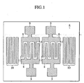
- a plurality of surface acoustic wave devices are simultaneously formed on a wafer.
- the surface acoustic wave device has a piezoelectric substrate 4 and a metal film having a predetermined shape arranged on the piezoelectric substrate 4.
- the metal film has two pairs of comb-teeth-shaped metal electrodes 8 mating with each other, electrode pads 9 connected to the metal electrodes 8, respectively, and reflectors 10 arranged on opposite ends of the metal electrodes 8.
- the metal electrodes 8 have electrode fingers 11 forming the mating comb-teeth parts. To the electrode pads 9, signal input/output terminals of the surface acoustic wave device are connectable.
- the reflectors 10 consist of a plurality of metals each having a rectangular plan shape with a large longitudinal-to-lateral ratio.
- the piezoelectric substrate 4 is a lithium tantalate (LiTaO 3 ) substrate.
- the metal film is made of 99.5 w/t % aluminum (Al) added with 0.5 w/t % copper (Cu).
- plan dimensions i.e., longitudinal and lateral dimensions of the electrode fingers 11 and the dimension of a gap between the adjacent electrode fingers 11 are precisely controlled by a known patterning technique.
- variable-velocity film forming process (S3) and fixed-velocity film forming process (S4) will be explained in detail in terms of the erosion diameter.
- an ordinate represents the erosion diameter (with standardized values) and an abscissa represents elapsed time. Values of the erosion diameter are standardized with the erosion diameter of the A-mode serving as 1. As explained above, the erosion diameter is adjustable according to the strength of a magnetic field parallel to a target surface.
- the erosion diameter (RE) is set to 3.6 in the E-mode (S31). Continuously thereafter, the erosion diameter (RE) is set to 4.6 in the F-mode (S32). In the E-mode (S33), the erosion diameter (RE) is set to 3.6. In the A-mode (S34), the erosion diameter (RE) is set to 1.0. These temporal erosion diameter changes form a cycle and are repeated seven times. After the completion of seven cycles, the erosion diameter (RE) is set to 3.6 in the E-mode (S4). In this way, the erosion diameter (RE) is cyclically changed, to achieve the variable-velocity film forming process (S3) and fixed-velocity film forming process (S4) shown in Fig. 3 .
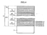
- Figure 4 shows a structure of the metal film 3 before carrying out the patterning process of step S6.
- the metal film 3 consists of a film formed by the variable-velocity film forming process (S3) and a film formed by the fixed-velocity film forming process (S4).
- the film by the variable-velocity film forming process (S3) is formed, and thereon, the film by the fixed-velocity film forming process (S4) is formed.
- the film by the variable-velocity film forming process (S3) consists of a plurality of films formed in the first through seventh cycles, respectively.
- the film of each cycle further consists of a plurality of films formed in steps S31 through S34, respectively.
- the film formed in step S31 in the E-mode involves substantially no film thickness difference between the central and peripheral parts of the wafer 2.
- S32(F-mode) film a film thickness at the central part of the wafer 2 is thinner than a film thickness at the peripheral part thereof.
- the S33(E-mode) film is like the S31(E-mode) film.
- S34(A-mode) film a film thickness at the central part of the wafer 2 is thicker than a film thickness at the peripheral part thereof. In this way, the films formed in the respective film-forming modes have different in-wafer-plane film-thickness distributions.
- the first-cycle (S31 through S34) film has substantially no film thickness difference between the central and peripheral parts of the wafer 2 and shows an even in-wafer-plane film-thickness distribution.
- the second- to seventh-cycle films are like the first-cycle film. Namely, combining two or more film-forming modes (A-mode and F-mode) involving uneven in-wafer-plane film-thickness distributions and a film-forming mode (E-mode) involving an even in-wafer-plane film-thickness distribution equalizes the in-wafer-plane film-thickness distribution of a metal film formed in one cycle.
- the film-forming modes (A-mode and F-mode) have opposite film-thickness distributions.
- the A-mode has a film-forming velocity Vc at the central part of the wafer 2 faster than a film-forming velocity Vp at the peripheral part of the wafer 2, and the F-mode shows the film-forming velocity Vc slower than the film-forming velocity Vp.
- the case explained here forms a cycle from three film-forming modes, i.e., the A-mode, F-mode, and E-mode. It is possible to exclude, from a cycle, the film-forming mode (E-mode) showing an even in-wafer-plane film-thickness distribution and form a cycle with two or more film-forming modes (A-mode and F-mode) showing uneven in-wafer-plane film-thickness distributions. In this case, adjusting a film forming time of each mode will equalize the in-wafer-plane film-thickness distribution of a metal film formed in each cycle.
- the thickness of the metal film 3 to be formed is 185 nm and each cycle forms a film of 25 nm thick.
- the above-mentioned cycle is repeated seven times.
- variable-velocity film forming process (S3) capable of forming a metal film having an even in-wafer-plane film-thickness distribution is employed to form the metal film 3 up to nearly the required film thickness
- the fixed-velocity film forming process (S4) is employed to carry out a final fine film thickness adjustment on the metal film 3.
- a film forming time of each of the film-forming modes (A-mode, F-mode, and E-mode) constituting the cycle must be adjusted. Namely, it is necessary to grasp, in advance, how the in-wafer-plane film-forming-velocity distribution of each film-forming mode is.
- a film-forming mode used in the fixed-velocity film forming process (S4) to carry out a final fine adjustment on the thickness of the metal film 3 is preferably required to have a sufficiently low film-forming velocity. Accordingly, the inventor measured the in-wafer-plane film-forming-velocity distribution of each film-forming mode.
- the measurement was carried out on a plurality of film-forming modes having different erosion diameters.
- a metal film Al film
- Al film Al film
- Erosion diameters were controlled with current values applied to an electromagnet for sputtering.
- a measuring apparatus used was profilometer (maker: KLA Tencor, model: P-10). The profilometer scans a wafer with a probe to measure irregularities on the surface of the wafer. The probe moves up and down in response to irregularities on the surface, to change the value of a capacitance attached to a base of the probe. The capacitance value change is read as an electric signal, to measure the irregularities on the surface. The same location on the wafer was measured 10 times and an average thereof was calculated.
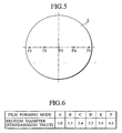
- film thickness measuring locations are five including a central part P3 of a wafer 2 having a radius of 50 mm, peripheral parts (P1 and P5) 40 mm from the central part, and intermediate parts (P2 and P4) 20 mm from the central part.
- film-thickness distributions were measured for six film-forming modes A through F. Erosion diameters (standardized values) of the film-forming modes are as shown in Fig. 6 . Each erosion diameter value is a standardized value with a value of the A-mode serving as 1.
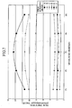
- a film-thickness distribution in the A-mode having the smallest erosion diameter shows a thicker film thickness at the wafer central part than at the peripheral parts and a largest film thickness difference compared with the other film-forming modes.
- a film-forming velocity over the wafer in the A-mode is fastest among all modes.
- a film-thickness distribution of the F-mode having the largest erosion diameter shows that a film thickness at the wafer central part is thinner than those at the peripheral parts and a film-forming velocity over the wafer is slowest among all modes.
- the film thickness values are standardized according to a film thickness value at the coordinates of the location P3 formed in the F-mode.
- a film-forming velocity of the film-forming mode used in the fixed-velocity film forming process (S4) must be equal to or lower than 150 nm per minute, and preferably, equal to or lower than 100 nm per minute.
- This film-forming velocity is an average of film-forming velocities at the wafer central part (P3) and peripheral parts (P1 and P5).
- ) in the fixed-velocity film forming process (S4) is preferably equal to or lower than 12%, and more preferably, equal to or lower than 11%.
- Film-forming modes that satisfy the above-mentioned film-forming conditions in the fixed-velocity film forming process are the D-mode, E-mode, and F-mode. Among them, the embodiment has selected the E-mode. Accordingly, instead of the E-mode, the D-mode or the F-mode may be employed in the fixed-velocity film forming process.
- forming a part of the metal film 3 in two or more film-forming modes (A-mode, E-mode, and F-mode) having different in-wafer-plane film-thickness distributions (variable-velocity film forming process) is capable of precisely controlling the in-wafer-plane film-thickness distribution of the part of the metal film 3.
- Forming the remaining part of the metal film 3 under a fixed film-forming condition (E-mode) is capable of precisely controlling the final thickness of the metal film 3.
- the materials and properties of the parts such as the piezoelectric substrate 4 mentioned in the embodiment are only examples and they are replaceable to provide the same effect of the present invention.
- the material of the piezoelectric substrate 4 is lithium tantalate (LiTaO 3 ).
- the substrate may be a lithium niobate (LiNbO 3 ) substrate, a lithium barate (LiB 4 O 7 ) substrate, or a piezoelectric substrate made of other material such as sapphire and crystal.
- the embodiment has been explained in connection with a metal film made of an alloy of 99.5 w/t % Al and 0.5 w/t % Cu.
- an electrode film made of Al without additives, or with an additive of other metal, or with a composition ratio different from the above-mentioned values.
- a metal film is directly formed on a piezoelectric substrate 4. It is possible to form, between the piezoelectric substrate 4 and the metal film, a barrier metal film made of, for example, titanium (Ti) or tantalum (Ta).
- variable-velocity film forming process is cyclically carried out, and then, the fixed-velocity film forming process is carried out.
- the fixed-velocity film forming process may be carried out first, and then, the variable-velocity film forming process may be carried out.
- film-forming velocities were changed in order of the E-mode, F-mode, E-mode, and A-mode. The order may not be limited to this and may be changed.
- A-, E-, and F-modes other film-forming modes shown in Fig. 6 are employable.
- an erosion diameter is determined by adjusting the strength of a magnetic field in a sputtering apparatus.
- an erosion diameter may be determined by adjusting sputtering power of a magnetron-type sputtering apparatus.
Landscapes
- Physics & Mathematics (AREA)
- Acoustics & Sound (AREA)
- Engineering & Computer Science (AREA)
- Manufacturing & Machinery (AREA)
- Surface Acoustic Wave Elements And Circuit Networks Thereof (AREA)
- Physical Vapour Deposition (AREA)
Claims (6)
- Herstellungsverfahren für eine Oberflächenwellen-Vorrichtung, umfassend ein Ausbilden eines Metallfilms an einem piezoelektrischen Substrat (4) und gezieltes Entfernen des Metallfilms, um kammzahnartige Metallelektroden (8) auszubilden, wobei der Arbeitsablauf des Ausbildens des Metallfilms am piezoelektrischen Substrat umfasst:einen ersten Arbeitsablauf (S3) des Ausbildens von Filmen mittels Durchführen zweier oder mehrerer Filmausbildungsbetriebsarten (A, E, F), die unterschiedliche Filmausbildungsgeschwindigkeitsverteilungen in einer Wafer-Ebene involvieren, undeinen zweiten Arbeitsablauf (S4) für eine endgültige Feinfilmdickeneinstellung des Ausbildens eines Films in einer festen Filmausbildungsbetriebsart, die eine ebene Filmdickenverteilung in einer Wafer-Ebene involviert.
- Herstellungsverfahren für eine Oberflächenwellen-Vorrichtung gemäß Anspruch 1, bei dem die zwei oder mehreren Filmausbildungsbetriebsarten (A, E, F) unterschiedliche Filmausbildungsgeschwindigkeitsverteilungen in einer Wafer-Ebene involvieren, umfassend:eine erste Filmausbildungsbetriebsart (A), bei der eine Filmausbildungsgeschwindigkeit an einem mittigen Teil des Wafers größer ist als diejenige an einem Umfangsteil des Wafers, undeine zweite Filmausbildungsbetriebsart (F), bei der eine Filmausbildungsgeschwindigkeit an einem mittigen Teil des Wafers geringer ist als diejenige an einem Umfangsteil des Wafers.
- Herstellungsverfahren für eine Oberflächenwellen-Vorrichtung gemäß Anspruch 2, bei dem die feste Filmausbildungsbetriebsart im zweiten Arbeitsablauf eine Filmausbildungsbetriebsart (E) ist, bei der eine durch Subtraktion einer Filmausbildungsgeschwindigkeit am Umfangsteil des Wafers von einer Filmausbildungsgeschwindigkeit an einem mittigen Teil des Wafers erhaltene Filmausbildungsgeschwindigkeitsdifferenz v kleiner ist als diejenige der ersten Filmausbildungsbetriebsart und größer als diejenige der zweiten Filmausbildungsbetriebsart.
- Herstellungsverfahren für eine Oberflächenwellen-Vorrichtung gemäß einem der vorangegangenen Ansprüche, bei dem beim ersten Arbeitsablauf (S3) die zwei oder mehreren Filmausbildungsbetriebsarten (A, E, F) zyklisch wiederholt werden.
- Herstellungsverfahren für eine Oberflächenwellen-Vorrichtung gemäß einem der vorangegangenen Ansprüche, bei dem beim zweiten Arbeitsablauf (S4) der Film in der Filmausbildungsbetriebsart bei einer durchschnittlichen Filmausbildungsgeschwindigkeit von 150 nm/min oder weniger ausgebildet wird.
- Herstellungsverfahren für eine Oberflächenwellen-Vorrichtung gemäß einem der vorangegangenen Ansprüche, bei dem(i) der Metallfilm mittels einer Magnetron-Bedampfungs-Technik ausgebildet wird,(ii) die im ersten Arbeitsablauf (S3) ausgebildeten Filme durch Verändern der Erosions-Durchmesser an einem Ziel ausgebildet werden, wodurch die Filmausbildungsgeschwindigkeitsverteilung in einer Wafer-Ebene verändert wird, und(iii) der im zweiten Arbeitsablauf (S4) ausgebildete Film bei einem festen Erosions-Durchmesser ausgebildet wird.
Applications Claiming Priority (3)
| Application Number | Priority Date | Filing Date | Title |
|---|---|---|---|
| JP2000191732 | 2000-06-26 | ||
| JP2000191732 | 2000-06-26 | ||
| PCT/JP2001/004814 WO2002001714A1 (fr) | 2000-06-26 | 2001-06-07 | Procede de fabrication d'un dispositif a ondes acoustiques de surface |
Publications (3)
| Publication Number | Publication Date |
|---|---|
| EP1306972A1 EP1306972A1 (de) | 2003-05-02 |
| EP1306972A4 EP1306972A4 (de) | 2008-10-15 |
| EP1306972B1 true EP1306972B1 (de) | 2009-11-04 |
Family
ID=18690982
Family Applications (1)
| Application Number | Title | Priority Date | Filing Date |
|---|---|---|---|
| EP01936895A Expired - Lifetime EP1306972B1 (de) | 2000-06-26 | 2001-06-07 | Verfahren zur herstellung eines oberflächenwellen-bauelements |
Country Status (7)
| Country | Link |
|---|---|
| US (1) | US6790321B2 (de) |
| EP (1) | EP1306972B1 (de) |
| JP (1) | JP4057907B2 (de) |
| KR (1) | KR100460218B1 (de) |
| CN (1) | CN1199351C (de) |
| DE (1) | DE60140367D1 (de) |
| WO (1) | WO2002001714A1 (de) |
Family Cites Families (4)
| Publication number | Priority date | Publication date | Assignee | Title |
|---|---|---|---|---|
| JPH03208888A (ja) | 1990-01-11 | 1991-09-12 | Nippon Telegr & Teleph Corp <Ntt> | スパッタリング方法 |
| JP3208888B2 (ja) | 1993-01-27 | 2001-09-17 | 株式会社村田製作所 | 液状樹脂組成物 |
| US5815900A (en) * | 1995-03-06 | 1998-10-06 | Matsushita Electric Industrial Co., Ltd. | Method of manufacturing a surface acoustic wave module |
| JP3430745B2 (ja) * | 1995-11-08 | 2003-07-28 | 松下電器産業株式会社 | Sawデバイス |
-
2001
- 2001-06-07 DE DE60140367T patent/DE60140367D1/de not_active Expired - Lifetime
- 2001-06-07 CN CNB018117686A patent/CN1199351C/zh not_active Expired - Fee Related
- 2001-06-07 JP JP2002505752A patent/JP4057907B2/ja not_active Expired - Fee Related
- 2001-06-07 US US10/297,950 patent/US6790321B2/en not_active Expired - Fee Related
- 2001-06-07 EP EP01936895A patent/EP1306972B1/de not_active Expired - Lifetime
- 2001-06-07 KR KR10-2002-7017630A patent/KR100460218B1/ko not_active Expired - Fee Related
- 2001-06-07 WO PCT/JP2001/004814 patent/WO2002001714A1/ja not_active Ceased
Also Published As
| Publication number | Publication date |
|---|---|
| KR100460218B1 (ko) | 2004-12-08 |
| US20030104136A1 (en) | 2003-06-05 |
| CN1439191A (zh) | 2003-08-27 |
| CN1199351C (zh) | 2005-04-27 |
| DE60140367D1 (de) | 2009-12-17 |
| EP1306972A4 (de) | 2008-10-15 |
| EP1306972A1 (de) | 2003-05-02 |
| KR20030011368A (ko) | 2003-02-07 |
| JP4057907B2 (ja) | 2008-03-05 |
| WO2002001714A1 (fr) | 2002-01-03 |
| US6790321B2 (en) | 2004-09-14 |
Similar Documents
| Publication | Publication Date | Title |
|---|---|---|
| EP0435189A2 (de) | Akustische Oberflächenwellenanordnung | |
| EP1391988B1 (de) | Oberflächenwellen-Bauelement und Verfahren zu seiner Herstellung | |
| KR20200078571A (ko) | 압전성 재료 기판과 지지 기판의 접합체, 그 제조 방법 및 탄성파 소자 | |
| US20150303895A1 (en) | Transducer with bulk waves surface-guided by synchronous excitation structures | |
| EP0064506B2 (de) | Verbesserungen von verfahren zum herstellen von bauelementen mit metallisierten bereichen auf dielektrischen substraten | |
| US5838090A (en) | Surface acoustic wave device | |
| US5320865A (en) | Method of manufacturing a surface acoustic wave device | |
| EP0688098B1 (de) | Akustische Oberflächenwellenanordnung von Diamant-LiTaO3 | |
| JPWO2011007690A1 (ja) | 弾性表面波装置 | |
| JP3318920B2 (ja) | 表面弾性波素子 | |
| US6810566B2 (en) | Method of manufacturing a surface acoustic wave element | |
| Iriarte et al. | SAW COM-parameter extraction in AlN/diamond layered structures | |
| JPH0998059A (ja) | 表面弾性波素子 | |
| Spencer | Monolithic crystal filters | |
| US6603371B2 (en) | Surface acoustic wave device having a small acoustic velocity distribution and method of producing the same | |
| US6483224B1 (en) | Surface acoustic wave device and method of producing the same | |
| EP1306972B1 (de) | Verfahren zur herstellung eines oberflächenwellen-bauelements | |
| WO2020038667A1 (en) | Tf-saw transducer with improved suppression of unwanted modes | |
| Fuentes Iriarte | AlN thin film electroacoustic devices | |
| JPWO2002001714A1 (ja) | 弾性表面波装置の製造方法 | |
| Callaghan et al. | Beam-supported AlN thin film bulk acoustic resonators | |
| Kadota et al. | Properties of zinc oxide films deposited by a radio‐frequency magnetron mode electron cyclotron resonance sputtering system | |
| JP3365505B2 (ja) | 表面弾性波素子 | |
| Henrot et al. | Ridge-shaped periodically poled transducer for wide band RF filter | |
| JPH09148879A (ja) | 弾性表面波デバイス |
Legal Events
| Date | Code | Title | Description |
|---|---|---|---|
| PUAI | Public reference made under article 153(3) epc to a published international application that has entered the european phase |
Free format text: ORIGINAL CODE: 0009012 |
|
| 17P | Request for examination filed |
Effective date: 20030121 |
|
| AK | Designated contracting states |
Designated state(s): DE FR GB |
|
| AX | Request for extension of the european patent |
Extension state: AL LT LV MK RO SI |
|
| A4 | Supplementary search report drawn up and despatched |
Effective date: 20080915 |
|
| 17Q | First examination report despatched |
Effective date: 20081124 |
|
| GRAP | Despatch of communication of intention to grant a patent |
Free format text: ORIGINAL CODE: EPIDOSNIGR1 |
|
| GRAS | Grant fee paid |
Free format text: ORIGINAL CODE: EPIDOSNIGR3 |
|
| GRAA | (expected) grant |
Free format text: ORIGINAL CODE: 0009210 |
|
| AK | Designated contracting states |
Kind code of ref document: B1 Designated state(s): DE FR GB |
|
| REG | Reference to a national code |
Ref country code: GB Ref legal event code: FG4D |
|
| REF | Corresponds to: |
Ref document number: 60140367 Country of ref document: DE Date of ref document: 20091217 Kind code of ref document: P |
|
| PGFP | Annual fee paid to national office [announced via postgrant information from national office to epo] |
Ref country code: FR Payment date: 20100709 Year of fee payment: 10 |
|
| PLBE | No opposition filed within time limit |
Free format text: ORIGINAL CODE: 0009261 |
|
| STAA | Information on the status of an ep patent application or granted ep patent |
Free format text: STATUS: NO OPPOSITION FILED WITHIN TIME LIMIT |
|
| 26N | No opposition filed |
Effective date: 20100805 |
|
| PGFP | Annual fee paid to national office [announced via postgrant information from national office to epo] |
Ref country code: GB Payment date: 20100602 Year of fee payment: 10 Ref country code: DE Payment date: 20100602 Year of fee payment: 10 |
|
| GBPC | Gb: european patent ceased through non-payment of renewal fee |
Effective date: 20110607 |
|
| REG | Reference to a national code |
Ref country code: FR Ref legal event code: ST Effective date: 20120229 |
|
| REG | Reference to a national code |
Ref country code: DE Ref legal event code: R119 Ref document number: 60140367 Country of ref document: DE Effective date: 20120103 |
|
| PG25 | Lapsed in a contracting state [announced via postgrant information from national office to epo] |
Ref country code: FR Free format text: LAPSE BECAUSE OF NON-PAYMENT OF DUE FEES Effective date: 20110630 Ref country code: DE Free format text: LAPSE BECAUSE OF NON-PAYMENT OF DUE FEES Effective date: 20120103 |
|
| PG25 | Lapsed in a contracting state [announced via postgrant information from national office to epo] |
Ref country code: GB Free format text: LAPSE BECAUSE OF NON-PAYMENT OF DUE FEES Effective date: 20110607 |