EP1306888A2 - Semiconductor processing apparatus for continuously forming semiconductor film on flexible substrate - Google Patents
Semiconductor processing apparatus for continuously forming semiconductor film on flexible substrate Download PDFInfo
- Publication number
- EP1306888A2 EP1306888A2 EP02016312A EP02016312A EP1306888A2 EP 1306888 A2 EP1306888 A2 EP 1306888A2 EP 02016312 A EP02016312 A EP 02016312A EP 02016312 A EP02016312 A EP 02016312A EP 1306888 A2 EP1306888 A2 EP 1306888A2
- Authority
- EP
- European Patent Office
- Prior art keywords
- flexible substrate
- heating
- heating device
- etching
- semiconductor film
- Prior art date
- Legal status (The legal status is an assumption and is not a legal conclusion. Google has not performed a legal analysis and makes no representation as to the accuracy of the status listed.)
- Withdrawn
Links
Images



Classifications
-
- H—ELECTRICITY
- H10—SEMICONDUCTOR DEVICES; ELECTRIC SOLID-STATE DEVICES NOT OTHERWISE PROVIDED FOR
- H10P—GENERIC PROCESSES OR APPARATUS FOR THE MANUFACTURE OR TREATMENT OF DEVICES COVERED BY CLASS H10
- H10P14/00—Formation of materials, e.g. in the shape of layers or pillars
- H10P14/20—Formation of materials, e.g. in the shape of layers or pillars of semiconductor materials
-
- H—ELECTRICITY
- H10—SEMICONDUCTOR DEVICES; ELECTRIC SOLID-STATE DEVICES NOT OTHERWISE PROVIDED FOR
- H10P—GENERIC PROCESSES OR APPARATUS FOR THE MANUFACTURE OR TREATMENT OF DEVICES COVERED BY CLASS H10
- H10P72/00—Handling or holding of wafers, substrates or devices during manufacture or treatment thereof
- H10P72/04—Apparatus for manufacture or treatment
- H10P72/0478—Apparatus for manufacture or treatment the substrates being processed being not semiconductor wafers, e.g. leadframes or chips
-
- C—CHEMISTRY; METALLURGY
- C23—COATING METALLIC MATERIAL; COATING MATERIAL WITH METALLIC MATERIAL; CHEMICAL SURFACE TREATMENT; DIFFUSION TREATMENT OF METALLIC MATERIAL; COATING BY VACUUM EVAPORATION, BY SPUTTERING, BY ION IMPLANTATION OR BY CHEMICAL VAPOUR DEPOSITION, IN GENERAL; INHIBITING CORROSION OF METALLIC MATERIAL OR INCRUSTATION IN GENERAL
- C23C—COATING METALLIC MATERIAL; COATING MATERIAL WITH METALLIC MATERIAL; SURFACE TREATMENT OF METALLIC MATERIAL BY DIFFUSION INTO THE SURFACE, BY CHEMICAL CONVERSION OR SUBSTITUTION; COATING BY VACUUM EVAPORATION, BY SPUTTERING, BY ION IMPLANTATION OR BY CHEMICAL VAPOUR DEPOSITION, IN GENERAL
- C23C14/00—Coating by vacuum evaporation, by sputtering or by ion implantation of the coating forming material
- C23C14/22—Coating by vacuum evaporation, by sputtering or by ion implantation of the coating forming material characterised by the process of coating
- C23C14/56—Apparatus specially adapted for continuous coating; Arrangements for maintaining the vacuum, e.g. vacuum locks
- C23C14/562—Apparatus specially adapted for continuous coating; Arrangements for maintaining the vacuum, e.g. vacuum locks for coating elongated substrates
-
- C—CHEMISTRY; METALLURGY
- C23—COATING METALLIC MATERIAL; COATING MATERIAL WITH METALLIC MATERIAL; CHEMICAL SURFACE TREATMENT; DIFFUSION TREATMENT OF METALLIC MATERIAL; COATING BY VACUUM EVAPORATION, BY SPUTTERING, BY ION IMPLANTATION OR BY CHEMICAL VAPOUR DEPOSITION, IN GENERAL; INHIBITING CORROSION OF METALLIC MATERIAL OR INCRUSTATION IN GENERAL
- C23C—COATING METALLIC MATERIAL; COATING MATERIAL WITH METALLIC MATERIAL; SURFACE TREATMENT OF METALLIC MATERIAL BY DIFFUSION INTO THE SURFACE, BY CHEMICAL CONVERSION OR SUBSTITUTION; COATING BY VACUUM EVAPORATION, BY SPUTTERING, BY ION IMPLANTATION OR BY CHEMICAL VAPOUR DEPOSITION, IN GENERAL
- C23C16/00—Chemical coating by decomposition of gaseous compounds, without leaving reaction products of surface material in the coating, i.e. chemical vapour deposition [CVD] processes
- C23C16/44—Chemical coating by decomposition of gaseous compounds, without leaving reaction products of surface material in the coating, i.e. chemical vapour deposition [CVD] processes characterised by the method of coating
- C23C16/54—Apparatus specially adapted for continuous coating
- C23C16/545—Apparatus specially adapted for continuous coating for coating elongated substrates
Definitions
- the present invention relates to a semiconductor processing apparatus for continuously forming a semiconductor film on a flexible substrate.
- a first prior art as shown in, for example, FIG. 4 is known as a conventional method for forming a semiconductor film on a substrate, as disclosed in Jpn. Pat. Appln. KOKAI Publication No. 8-293466.
- a reference numeral 1 shown in FIG. 4 denotes a tray for disposing thereon a planar irradiating substrate 2 to be irradiated with light.
- the tray 1 is movable in a direction denoted by an arrow A.
- a base coat film 3 is formed on the irradiating substrate 2, and an amorphous silicon film 4 is formed on the base coat 3.
- the surface of the irradiating substrate 2 is irradiated with a laser light C emitted from a laser oscillator 5 and having a high energy density. As shown in the drawing, the laser light C passes through a reflector 6 and a beam shaping unit 7 so as to permit the irradiating substrate 2 to be irradiated with the laser light C.
- an irradiating light B having an energy density lower than that of the laser light C is emitted from a high intensity light unit 9 equipped with an ultraviolet light unit 8 so as to permit the irradiating substrate 2 to be irradiated with the irradiating light B.
- the irradiating substrate 2 is irradiated with both the laser light C having a high energy density and the laser light B emitted from the high intensity light unit 9 and having an energy density lower than that of the laser light C so as to heat the amorphous silicon film 4 formed on the base coat film 3 and, thus, to convert the amorphous silicon film 4 into a polycrystalline silicon (polysilicon) film.
- FIG. 5 A second prior art shown in FIG. 5, which is disclosed in Japanese Patent Disclosure No. 10-270359, is also known as a conventional method for forming a semiconductor thin film on a substrate.
- a reference numeral 11 shown in FIG. 5 denotes a sample.
- the sample 11 is constructed such that an insulating film 13, a thin film semiconductor film 14, an insulating film 15, a thin film semiconductor film 16 and an insulating film 17 are formed in the order mentioned on a planar substrate 12.
- molten portions 18 and 19 are formed in the thin semiconductor films 14 and 16, respectively.
- recrystallized semiconductor portions 20 and 21 are also formed in the thin semiconductor films 14 and 16, respectively.
- a base heating source 22 for performing the function of heating the entire sample 11 is arranged below the sample 11. Also, a melt heating source 23 is arranged above the sample 11. The infrared rays generated from the melt heating source 23 pass through an elliptical mirror 24 so as to be converged on a prescribed portion on the sample 11.
- the temperature of the melt heating source 23 such as an infrared halogen lamp is elevated under the state that the temperature of the base heating source 23 is elevated so as to heat the entire sample 11 to a temperature not higher than the melting point of silicon, e.g., 100°C to 1,400°C.
- the infrared rays generated by the heating of the melt heating source 23 are focused by the elliptical mirror 24 so as to heat and melt dot-like points of the thin semiconductor films 14 and 16 that are to be melted for recrystallization, thereby forming the molten portions 18 and 19.
- a semiconductor film which is not of a single crystalline structure, is irradiated with a laser light or an electron beam so as to increase the crystal grain size of the thin film, to convert the crystal structure into a single crystalline structure, to laminate thin films, or to carry out a lithography.
- each of these prior arts is directed to a process that is carried out on a rigid planar substrate.
- an apparatus for forming a semiconductor film on a flexible substrate has not yet been developed.
- the prior art is directed to an apparatus for carrying out the processing on the basis of a batch system in which the substrate such as a semiconductor wafer is processed one by one. In other words, the conventional apparatus is incapable of performing a continuous processing efficiently.
- An object of the present invention is to provide an apparatus for forming a semiconductor film continuously on a flexible substrate, which permits continuously performing a series of steps ranging between the formation of an amorphous silicon thin film on a flexible substrate and the recrystallization of the amorphous silicon thin film to form a laminate structure of single crystalline silicon films.
- an apparatus for forming a semiconductor film on a flexible substrate comprising a supply device for supplying a flexible substrate; a recovery device for recovering the flexible substrate; a first heating device arranged between the supply device arid the recovery device for heating the substrate; a PVD device for depositing a film on the substrate by a physical vapor deposition; a CVD device for depositing a film on the substrate by a chemical vapor deposition; a second heating device for heating the material deposited on the substrate; and an etching device for etching the material deposited on the substrate, wherein the CVD device, the second heating device and the etching device are repeatedly arranged within a casing held under a prescribed atmosphere.
- the apparatus of the present invention for forming a semiconductor film on a flexible substrate comprises a supply device for supplying a flexible substrate; a recovery device for recovering the flexible substrate; a first heating device arranged between said supply device and said recovery device for heating said substrate; a PVD device for depositing a film on said substrate by a physical vapor deposition; a CVD device for depositing a film on said substrate by a chemical vapor deposition; a second heating device for heating the material deposited on said substrate; and an etching device for etching the material deposited on said substrate, wherein said CVD device, said second heating device and said etching device are repeatedly arranged within a casing held under a prescribed atmosphere.
- a radiation heat type or a laser type heating device is used as the second heating device, and an optical etching device is used as the etching device.
- an exhaust chamber is arranged between the first heating device and the PCD device, between the PVD device and the CVD device, between the DVD device and the second heating device, and between the second heating device and the etching device.
- a floating roll for determining the position of the flexible substrate is arranged between the first heating device and the PVD device, between the PVD device and the CVD device, between the CVD device and the second heating device, and between the second heating device and the etching device.
- the flexible substrate is formed of any of a thin metal sheet and a thin plastic sheet.
- a roll for applying each processing to the flexible substrate is arranged in each of the chambers housing the first heating device, the PVD device, the CVD device, the second heating device, and the etching device. Also, the roll noted above has a surface roughness not larger than 0.3 ⁇ m.
- the present invention covers the case where the second heating device is a radiation heat type or laser type heating device, and the etching device is an optical etching device.
- an exhaust chamber between the first heating device and the PVD device, between the PVD device and the CVD device, between the CVD device and the second heating device, and between the second heating device and the etching device.
- the exhaust chamber thus arranged permits avoiding the mixing of the process gasses supplied to the process chambers.
- a floating roll for determining the position of the flexible substrate between the first heating device and the PVD device, between the PVD device and the CVD device, between the CVD device and the second heating device, and between the second heating device and the etching device.
- the floating roll thus arranged permits determining the position for applying the processing to the flexible substrate.
- the flexible substrate is formed of a thin metal sheet such as a thin stainless steel sheet or a thin plastic sheet.
- the particular thin sheet is excellent in the ductility and in the heat resistance or heat insulating properties. It follows that the flexible substrate formed of the particular thin sheet is adapted for the process such as a local heating.
- the present invention it is desirable to arrange a roll for applying each processing to the flexible substrate in each of the chambers housing the first heating device, the PVD (physical vapor deposition) device, the CVD (chemical vapor deposition) device, the second heating device, and the etching device. It is also desirable for the surface roughness of the roll to be set at a level not higher than 0.3 ⁇ m. Where the surface roughness of the roll is set at a level not higher than 0.3 ⁇ m, it is possible to maintain uniform the temperature of the flexible substrate and to make uniform the contact heat transmission to the substrate. If the surface roughness of the roll exceeds 0.3 ⁇ m, it is impossible to obtain sufficient effects.
- the present invention provides an apparatus for forming continuously a semiconductor film on a flexible substrate in place of the conventional apparatus for forming a semiconductor film on a batch system.
- the apparatus of the present invention permits consecutively performing a series of steps ranging between the step of forming an amorphous silicon thin film on a flexible substrate and the step of crystallizing the amorphous silicon thin film so as to form a multi-layer structure consisting of a plurality of single crystalline silicon films on the flexible substrate.
- the present invention provides an apparatus for forming a semiconductor film on a flexible substrate, which permits producing various effects, including, for example, that (1) it is possible to prevent an unnecessary gaseous components from being carried into the process chamber, (2) a series of process steps can be carried out while preventing the laminate structure of the semiconductor films from being contaminated with the air, (3) the process position can be determined by the fine adjustment of the floating roll, (4) the process chamber gas can be prevented from entering the exhaust chamber gas on the side of the front stage and the exhaust chamber gas on the side of the rear stage so as to permit the waste process chamber gas to be evacuated efficiently, (5) the flexible substrate passing along the outer circumferential surface of the process roll can be heated to the temperature required for the processing, (6) the unnecessary gas or the like after the processing in each process section can be evacuated to the outside through an exhaust port so as to decrease the amount of the waste gas in the exhaust chamber, (7) even if the amount of the thermal expansion of the flexible substrate within a certain process chamber differs from that in another process chamber, it is possible for the floating
- FIG. 1 schematically shows the entire construction of an apparatus for forming a semiconductor film on a flexible substrate
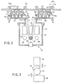
- FIG. 2 shows in a magnified fashion a gist portion of the apparatus shown in FIG. 1
- FIG. 3 shows in a magnified fashion a gist portion of the apparatus shown in FIG. 2.
- the apparatus of the present invention for forming a semiconductor film on a flexible substrate is housed in a series of continuous casings in which a prescribed atmosphere is maintained.
- the semiconductor film forming apparatus comprises a pay-off section 31, which is arranged on the side of one end of the semiconductor film forming apparatus and used as a supply device for supplying a flexible substrate 32 formed of a polyimide film into each process section, and a wind-up section 34, which is arranged on the side of the other end of the semiconductor film forming apparatus and used as a recovery device for recovering the flexible substrate.
- the pay-off section 31 comprises a pay-off reel 33 held under a clean atmosphere free from dust for winding up the flexible substrate 32.
- the wind-up section 34 comprises a wind-up reel 35 arranged under a clean atmosphere free from dust for winding up the processed flexible substrate 32.
- a first heating device 36 Arranged between the pay-off section 31 and the wind-up section 34 are a first heating device 36, a PVD device 37, CVD devices 38, 41, laser type second heating devices 39, 42, optical etching devices 40, 43 and an additional treatment device 44.
- the first heating device 36 performs the function of heating the flexible substrate 32.
- the PVD device 37 performs the function of physically depositing a film on the flexible substrate 32 by a physical vapor deposition.
- the CVD devices 38 and 41 perform the function of depositing a film on the flexible substrate 32 by a chemical vapor deposition.
- the second heating devices 39 and 42 perform the function of heating the material deposited on the flexible substrate 32.
- the optical etching devices 40 and 43 perform the function of etching the material deposited on the flexible substrate 32.
- the CVD devices, the second heating devices and the etching devices are repeatedly arranged n-times in the direction of the flow of the flexible substrate 32. Each of these devices 36 to 43 is held under the atmosphere required
- the deposition of a first semiconductor film on the flexible substrate 32, the annealing of the first semiconductor film by irradiation with a laser beam (or EB), and the laser etching are performed by the CVD device 38, the second heating device 39 and the etching device 40, respectively.
- the deposition of a second semiconductor film on the flexible substrate 32, the annealing of the first semiconductor film by irradiation with a laser beam (or EB), and the laser etching are performed by the CVD device 41, the second heating device 42 and the etching device 43, respectively.
- various types of processing are successively applied to the semiconductor films formed on the flexible substrate so as to finally apply various types of processing to the n-th semiconductor film formed on the flexible substrate.
- the flexible substrate 32 having an additional treatment applied thereto in the final stage is wound up by the wind-up reel 35 arranged in the wind-up section 32.
- exhaust sections 45a, 45b, 45c, 45d, 45e, 45f, 45g, 45h, 45i, ... 45n are arranged between adjacent process sections, i.e., between the pay-off section 31 and the first heating device 36, between the first heating device 36 and the PVD device 37, between the PVD device 37 and the CVD device 38, between the CVD device 38 and the second heating device 39, between the second heating device 39 and the etching device 40, between the etching device 40 and the CVD device 41, between the CVD device 41 and the second heating device 42, between the second heating device 42 and the wind-up etching device 43, and between the additional treatment device 44 and the wind-up section 34, respectively.
- the sealing function between the adjacent process sections e.g., the sealing function in the first heating device 36
- the process sections other than the first heating device 36 also perform a similar sealing function.
- a casing 51 is filled with a process chamber gas 52.
- a process roll 54 equipped with a heating device 53 and a heater 55 are arranged inside the casing 51, and the casing 51 is exhausted through an exhaust port 56.
- the surface roughness of the process roll 54 is set at 0.3 ⁇ m or less in order to maintain uniform the temperature of the flexible substrate 32, thereby making the contact heat transmission uniform.
- Four sealing rolls 57 are arranged apart from each other in an exhaust section 45a on the upstream side (the upper side in the drawing) of the first heating device 36.
- four upper side sealing bars 58 are arranged upstream of the four sealing rolls 57, and four lower side sealing bars 60 are arranged downstream of the four sealing rolls 57.
- the flexible substrate 32 is allowed to pass through the clearance between the sealing roll 57 and the upper side sealing bar 58.
- the flexible substrate 32 passes through the clearance between the sealing roll 57 and the upper side sealing bar 58 so as to reach the process roll 54 through a floating roll 61a serving to determine the fine positioning of the flexible substrate 32.
- the floating roll 61a is set movable in a direction perpendicular to the main surface of the flexible substrate 32, i.e., in the direction denoted by an arrow X in the drawing.
- the exhaust section 45a is divided into three chambers by the sealing roll 57, the upper side sealing bar 58 and the lower side sealing bar 60.
- FIG. 3 shows the clearance between the upper side sealing bar 58 and the sealing roll 57 and the clearance between the sealing roll 57 and the lower side sealing bar 60.
- the clearance L 1 between the upper side sealing bar 58 and the upper surface of the flexible substrate 32 is set at 0.15 mm and, thus, the clearance between the upper side sealing bar 58 and the sealing roll 57 is set equal to the sum of the clearance L 1 , i.e., 0.15 mm, and the thickness of the flexible substrate 32.
- the lower side clearance L 2 between the lower side sealing bar 60 and the sealing roll 57 is set at 0.15 mm.
- deflector rolls 59 are arranged adjacent to the prescribed upper side sealing bars 58 on the upper side of the flexible substrate 32 so as to prevent the flexible substrate 32 from being brought into contact with the upper side sealing bars 58. It should be noted that these deflector rolls 59 serve to hold the flexible substrate 32 on the side of the sealing rolls 58.
- Each exhaust chamber is provided with an exhaust port 67.
- the apparatus is constructed such that the process chamber gas 52, which is capable of entering the exhaust chamber on the side of the process chamber and the central exhaust chamber, is incapable of entering the exhaust chamber on the front stage and the exhaust chamber on the rear stage. Also, the apparatus is capable of evacuating the waste process chamber gas to the outside through the exhaust ports 67.
- the flexible substrate 32 reaching the process roll 54 is heated by the heating device 53 to the temperature required for the processing. Also, the gas required for the processing or a metal vapor is released from the process device 36, and the unnecessary gas or the like is evacuated to the outside through the exhaust port 56.
- An exhaust section 45b downstream of the first heating device 36 (the right side in the drawing) is substantially equal in construction to the exhaust section 45a upstream of the first heating section 36.
- sealing rolls 62 are arranged apart from each other on the downstream side in the exhaust section 45b.
- sealing bars 63 are arranged on the upper side of the sealing rolls 62, and four lower side sealing bars 65 are arranged on the lower side of the sealing rolls 62. Further, the flexible substrate 32 passes through the clearance between the sealing rolls 62 and the upper side sealing bars 63.
- the flexible substrate 32 passes through a floating roll 61b serving to perform a fine positioning and, then, through the clearance between the sealing rolls 62 and the upper sealing bars 63 so as to reach the next process chamber.
- a floating roll 61b serving to perform a fine positioning and, then, through the clearance between the sealing rolls 62 and the upper sealing bars 63 so as to reach the next process chamber.
- the exhaust section 45b is divided into three chambers by the sealing rolls 62, the upper side sealing bars 63 and the lower side sealing bars 65.
- the clearance between the upper side sealing bar 63 and the upper surface of the flexible substrate 32 is set at 0.15 mm and, thus, the upper side clearance between the upper side sealing bar 63 and the sealing roll 62 is set equal to the sum of the clearance between the upper side sealing bar 63 and the upper surface of the flexible substrate 32, i.e., 0.15 mm, and the thickness of the flexible substrate 32.
- the lower clearance between the sealing roll 62 and the lower side sealing bar 65 is set at 0.15 mm. Therefore, it is possible to suppress the entry of the process gas into the upper and lower clearances.
- the flexible substrate 32 passing through the upper clearance is prevented from being brought into contact with the upper side sealing bar 63.
- deflector rolls 64 are arranged adjacent to the prescribed upper side sealing bars 63 so as to prevent the flexible substrate 32 from being brought into contact with the upper side sealing bars 63. These deflector rolls 64 serve to hold the flexible substrate 32 toward the sealing rolls 62.
- Each exhaust chamber is provided with three exhaust ports 68, and the apparatus is constructed such that the process chamber gas 52, which is capable of entering the exhaust chamber on the side of the process chamber and the central exhaust chamber, is incapable of entering the exhaust chamber on the front stage and the exhaust chamber on the rear stage.
- the apparatus is capable of discharging the waste process chamber gas 52 to the outside.
- a control sensor 69 is arranged on the downstream side of the floating roll 61b.
- the control sensor 69 serves to maintain constant the moving speed of the flexible substrate 32 within each process section while measuring the moving speed of the flexible substrate 32 and to prevent a nonuniform excessive tension from being applied to the flexible substrate 32.
- a reference numeral 70 shown in FIG. 2 denotes a casing
- reference numerals 71a and 71b denote the sealing section casings between the adjacent casings 70.
- the flexible substrate 32 is driven at a constant moving speed within each process section while the moving speed of the flexible substrate 32 is being measured by the control sensor 69 so as to prevent a nonuniform excessive tension from being applied to the flexible substrate 32.
- the flexible substrate is formed of a polyimide film.
- the flexible substrate is not limited to a polyimide film.
- a thin sheet such as a stainless steel sheet can also be used as the flexible substrate.
- the exhaust section includes three exhaust chambers.
- the exhaust section it is not absolutely necessary for the exhaust section to include three exhaust chambers.
- the exhaust section it is possible for the exhaust section to include only one exhaust chamber, depending on the allowable amount of impurity gas contained in the process gas.
- the exhaust section it is possible for the exhaust section to include four or five exhaust chambers in the case where the allowable amount of the impurity gas is severe.
Landscapes
- Chemical & Material Sciences (AREA)
- Chemical Kinetics & Catalysis (AREA)
- Engineering & Computer Science (AREA)
- Materials Engineering (AREA)
- Mechanical Engineering (AREA)
- Metallurgy (AREA)
- Organic Chemistry (AREA)
- General Chemical & Material Sciences (AREA)
- Chemical Vapour Deposition (AREA)
- Recrystallisation Techniques (AREA)
- Lasers (AREA)
- Physical Vapour Deposition (AREA)
Abstract
Description
Claims (6)
- An apparatus for forming a semiconductor film on a flexible substrate, characterized by comprising:wherein said CVD device (38), (40), said second heating device (39), (42) and said etching device (40), (43) are repeatedly arranged within a casing held under a prescribed atmosphere.a supply device (31) for supplying a flexible substrate (32);a recovery device (34) for recovering the flexible substrate (32);a first heating device (36) arranged between said supply device (31) and said recovery device (34) for heating said substrate (32) ;a PVD device (37) for depositing a film on said substrate (32) by a physical vapor deposition;a CVD device (38) for depositing a film on said substrate (32) by a chemical vapor deposition;a second heating device (39) for heating the material deposited on said substrate (32); andan etching device (40) for etching the material deposited on said substrate (32),
- The apparatus for forming a semiconductor film on a flexible substrate according to claim 1, characterized in that said second heating device (39), (42) is a radiation heat type or laser type heating device, and said etching device (40), (43) is an optical etching device.
- The apparatus for forming a semiconductor film on a flexible substrate according to any one of claim 1 and claim 2, characterized in that an exhaust chamber is arranged between said first heating device (36) and said PVD device (37), between said PVD device (37) and said CVD device (38), (41), between said CVD device (38), (41) and said second heating device (39), (42), and between said second heating device (39), (42) and said etching device (40), (43).
- The apparatus for forming a semiconductor film on a flexible substrate according to any one of claim 1 to claim 3, characterized in that a floating roll (61a), (61b) for determining the position of said flexible substrate (32) is arranged between said first heating device (36) and said PVD device (37), between said PVD device (37) and said CVD device (38), (41), between said CVD device (38), (41) and said second heating device (39), (42), and between said second heating device (39), (42) and said etching device (40), (43).
- The apparatus for forming a semiconductor film on a flexible substrate according to any one of claim 1 to claim 4, characterized in that said flexible substrate (32) is formed of any of a thin metal sheet and a thin plastic sheet.
- The apparatus for forming a semiconductor film on a flexible substrate according to any one of claim 1 to claim 5, characterized in that a roll (54) for applying a processing to said flexible substrate is arranged in each of the chambers housing said first heating device (36), said PVD device (37), said CVD device (38), (41), said second heating device (39), (42), and said etching device (40), (43), and the surface roughness of said roll (54) is not larger than 0.3 µm.
Applications Claiming Priority (2)
| Application Number | Priority Date | Filing Date | Title |
|---|---|---|---|
| JP2001331382 | 2001-10-29 | ||
| JP2001331382A JP2003133230A (en) | 2001-10-29 | 2001-10-29 | Semiconductor processing equipment for flexible substrates |
Publications (2)
| Publication Number | Publication Date |
|---|---|
| EP1306888A2 true EP1306888A2 (en) | 2003-05-02 |
| EP1306888A3 EP1306888A3 (en) | 2006-07-05 |
Family
ID=19146974
Family Applications (1)
| Application Number | Title | Priority Date | Filing Date |
|---|---|---|---|
| EP02016312A Withdrawn EP1306888A3 (en) | 2001-10-29 | 2002-07-24 | Semiconductor processing apparatus for continuously forming semiconductor film on flexible substrate |
Country Status (5)
| Country | Link |
|---|---|
| US (1) | US20030079837A1 (en) |
| EP (1) | EP1306888A3 (en) |
| JP (1) | JP2003133230A (en) |
| KR (1) | KR100473009B1 (en) |
| TW (1) | TW558780B (en) |
Cited By (2)
| Publication number | Priority date | Publication date | Assignee | Title |
|---|---|---|---|---|
| WO2009024460A3 (en) * | 2007-08-20 | 2009-05-07 | Novogenio S L | System and process for the continous vacuum coating of a material in web form |
| FR2940321A1 (en) * | 2008-12-19 | 2010-06-25 | Carewave Shielding Technologie | VACUUM DEPOSITION MACHINE ON SUBSTRATE OF THIN LAYER MATERIALS BY CATHODIC SPRAYING. |
Families Citing this family (16)
| Publication number | Priority date | Publication date | Assignee | Title |
|---|---|---|---|---|
| US6878207B2 (en) * | 2003-02-19 | 2005-04-12 | Energy Conversion Devices, Inc. | Gas gate for isolating regions of differing gaseous pressure |
| JP4923446B2 (en) * | 2005-06-20 | 2012-04-25 | ソニー株式会社 | Laser processing apparatus and laser processing method |
| US20070141843A1 (en) * | 2005-12-01 | 2007-06-21 | Tokyo Electron Limited | Substrate peripheral film-removing apparatus and substrate peripheral film-removing method |
| KR100728889B1 (en) | 2006-06-07 | 2007-06-20 | (주)에스엠씨 | Flexible film etching equipment |
| KR100728890B1 (en) * | 2006-06-07 | 2007-06-20 | (주)에스엠씨 | Flexible film etching equipment |
| JP2008081820A (en) * | 2006-09-28 | 2008-04-10 | Sumitomo Electric Ind Ltd | Deposition equipment |
| WO2008108036A1 (en) * | 2007-03-01 | 2008-09-12 | Sharp Kabushiki Kaisha | Substrate processing equipment and substrate processing method employing it |
| KR100886115B1 (en) * | 2007-05-22 | 2009-02-27 | 네오뷰코오롱 주식회사 | Flexible substrate, manufacturing method thereof, and flexible display device using same |
| KR20090088056A (en) * | 2008-02-14 | 2009-08-19 | 삼성전기주식회사 | Gas Supply Units and Chemical Vapor Deposition Devices |
| US8419857B2 (en) * | 2009-03-31 | 2013-04-16 | United Technologies Corporation | Electron beam vapor deposition apparatus and method of coating |
| CN102650046B (en) * | 2012-05-23 | 2013-08-21 | 徐明生 | Device for largely and continuously preparing two-dimensional nanometer films in large |
| WO2013149572A1 (en) * | 2012-04-02 | 2013-10-10 | Xu Mingsheng | Equipment for large-scale continuous preparation of two-dimensional nanometer thin film |
| CN102634776B (en) * | 2012-05-03 | 2014-03-12 | 徐明生 | Chemical vapor deposition device for continuously preparing two-dimensional nanofilm |
| JP5958092B2 (en) * | 2012-05-31 | 2016-07-27 | ソニー株式会社 | Film forming apparatus and film forming method |
| CN102732834B (en) * | 2012-06-18 | 2013-11-20 | 徐明生 | Apparatus for preparing two-dimensional nanometer film |
| CN103484825B (en) * | 2013-10-15 | 2016-01-13 | 汕头万顺包装材料股份有限公司 | A kind of sputter shaped device of conductive film |
Family Cites Families (19)
| Publication number | Priority date | Publication date | Assignee | Title |
|---|---|---|---|---|
| US2972330A (en) * | 1956-02-15 | 1961-02-21 | Nat Steel Corp | Vacuum seal for coating apparatus |
| US2989026A (en) * | 1957-11-19 | 1961-06-20 | Nat Steel Corp | Vacuum coating apparatus |
| US2952569A (en) * | 1958-01-28 | 1960-09-13 | Nat Steel Corp | Method and apparatus forming an ice seal in vapor deposition |
| BE792701A (en) * | 1971-12-14 | 1973-03-30 | Arbed | |
| US3807058A (en) * | 1972-12-20 | 1974-04-30 | Gaf Corp | Sealing arrangement for enclosed chamber |
| US4438723A (en) * | 1981-09-28 | 1984-03-27 | Energy Conversion Devices, Inc. | Multiple chamber deposition and isolation system and method |
| EP0130444B1 (en) * | 1983-06-17 | 1987-09-23 | Hitachi, Ltd. | Continuous vacuum treating apparatus |
| US4663829A (en) * | 1985-10-11 | 1987-05-12 | Energy Conversion Devices, Inc. | Process and apparatus for continuous production of lightweight arrays of photovoltaic cells |
| DE3627384A1 (en) * | 1986-08-12 | 1988-02-18 | Siemens Ag | INDIRECTLY HEATED STORAGE CATHODE, IN PARTICULAR METAL-CAPILLARY CATHODE, FOR ELECTRICAL DISCHARGE VESSELS |
| DE3641718A1 (en) * | 1986-12-06 | 1988-06-16 | Leybold Ag | METHOD FOR PRODUCING WRAPS FROM INSULATING FILMS COATED CONDUCTIVELY IN A VACUUM |
| US5192585A (en) * | 1987-05-20 | 1993-03-09 | Kawasaki Steel Corp. | Differential pressure sealing apparatus and method |
| US4763601A (en) * | 1987-09-02 | 1988-08-16 | Nippon Steel Corporation | Continuous composite coating apparatus for coating strip |
| DE4324320B4 (en) * | 1992-07-24 | 2006-08-31 | Fuji Electric Co., Ltd., Kawasaki | Method and device for producing a thin-film photovoltaic conversion device |
| US6171714B1 (en) * | 1996-04-18 | 2001-01-09 | Gould Electronics Inc. | Adhesiveless flexible laminate and process for making adhesiveless flexible laminate |
| KR100296692B1 (en) * | 1996-09-10 | 2001-10-24 | 사토 도리 | Plasma CVD |
| KR100284567B1 (en) * | 1997-04-15 | 2001-04-02 | 후지이 아키히로 | Vertical wafer boat |
| US6186090B1 (en) * | 1999-03-04 | 2001-02-13 | Energy Conversion Devices, Inc. | Apparatus for the simultaneous deposition by physical vapor deposition and chemical vapor deposition and method therefor |
| US6298685B1 (en) * | 1999-11-03 | 2001-10-09 | Applied Materials, Inc. | Consecutive deposition system |
| JP4316767B2 (en) * | 2000-03-22 | 2009-08-19 | 株式会社半導体エネルギー研究所 | Substrate processing equipment |
-
2001
- 2001-10-29 JP JP2001331382A patent/JP2003133230A/en not_active Withdrawn
-
2002
- 2002-07-24 EP EP02016312A patent/EP1306888A3/en not_active Withdrawn
- 2002-07-30 KR KR10-2002-0044887A patent/KR100473009B1/en not_active Expired - Fee Related
- 2002-07-30 US US10/207,023 patent/US20030079837A1/en not_active Abandoned
- 2002-07-31 TW TW091117147A patent/TW558780B/en active
Cited By (5)
| Publication number | Priority date | Publication date | Assignee | Title |
|---|---|---|---|---|
| WO2009024460A3 (en) * | 2007-08-20 | 2009-05-07 | Novogenio S L | System and process for the continous vacuum coating of a material in web form |
| ES2336870A1 (en) * | 2007-08-20 | 2010-04-16 | Novogenio, S.L. | System and process for the continous vacuum coating of a material in web form |
| ES2336870B1 (en) * | 2007-08-20 | 2011-02-18 | Novogenio, S.L. | SYSTEM AND PROCEDURE FOR EMPTY AND CONTINUOUS COATING OF A BAND-FORMED MATERIAL. |
| FR2940321A1 (en) * | 2008-12-19 | 2010-06-25 | Carewave Shielding Technologie | VACUUM DEPOSITION MACHINE ON SUBSTRATE OF THIN LAYER MATERIALS BY CATHODIC SPRAYING. |
| WO2010076419A1 (en) * | 2008-12-19 | 2010-07-08 | Carewave Shielding Technologies (Sas) | Machine for the vacuum deposition of materials into thin layers by cathode spraying |
Also Published As
| Publication number | Publication date |
|---|---|
| KR20030035825A (en) | 2003-05-09 |
| TW558780B (en) | 2003-10-21 |
| US20030079837A1 (en) | 2003-05-01 |
| EP1306888A3 (en) | 2006-07-05 |
| JP2003133230A (en) | 2003-05-09 |
| KR100473009B1 (en) | 2005-03-10 |
Similar Documents
| Publication | Publication Date | Title |
|---|---|---|
| US20030079837A1 (en) | Semiconductor processing apparatus for continuously forming semiconductor film on flexible substrate | |
| US7687380B2 (en) | Laser annealing method and laser annealing device | |
| US7986871B2 (en) | Processing multilayer semiconductors with multiple heat sources | |
| US5505779A (en) | Integrated module multi-chamber CVD processing system and its method for processing substrates | |
| US5862302A (en) | Thermal processing apparatus having a reaction tube with transparent and opaque portions | |
| US5259883A (en) | Method of thermally processing semiconductor wafers and an apparatus therefor | |
| US6150265A (en) | Apparatus for forming materials | |
| JP3393469B2 (en) | Thin film semiconductor device manufacturing method and thin film semiconductor forming apparatus | |
| JPH06260436A (en) | Method of manufacturing semiconductor device and semiconductor processing apparatus | |
| US12248243B2 (en) | Multilayer graphene direct growth method and method for manufacturing pellicle for extreme ultraviolet lithography using the same | |
| US20080296258A1 (en) | Plenum reactor system | |
| US5439850A (en) | Method for forming a layer of uniform thickness on a semiconductor wafer during rapid thermal processing | |
| JPH03148829A (en) | Heat-treating device | |
| US20050053369A1 (en) | Focused photon energy heating chamber | |
| US20240030038A1 (en) | Atomic layer etching (ale) apparatus and ale method based on the apparatus | |
| US6281122B1 (en) | Method for forming materials | |
| JP3612018B2 (en) | Method for manufacturing semiconductor device | |
| JP3612009B2 (en) | Method for manufacturing semiconductor device | |
| JPS6152231B2 (en) | ||
| JPH04180624A (en) | Formation of pattern | |
| JP3272610B2 (en) | Metal thin film forming method | |
| JP3605330B2 (en) | Method for manufacturing thin film device and semiconductor film | |
| JP2001040485A (en) | Composite treatment of film substrate and composite treating device | |
| JPH10116795A (en) | Equipment for manufacturing semiconductor material | |
| JPS63308910A (en) | Method for producing thin film by energy beam irradiation and apparatus used therein |
Legal Events
| Date | Code | Title | Description |
|---|---|---|---|
| PUAI | Public reference made under article 153(3) epc to a published international application that has entered the european phase |
Free format text: ORIGINAL CODE: 0009012 |
|
| 17P | Request for examination filed |
Effective date: 20020724 |
|
| AK | Designated contracting states |
Designated state(s): AT BE BG CH CY CZ DE DK EE ES FI FR GB GR IE IT LI LU MC NL PT SE SK TR |
|
| AX | Request for extension of the european patent |
Extension state: AL LT LV MK RO SI |
|
| PUAL | Search report despatched |
Free format text: ORIGINAL CODE: 0009013 |
|
| AK | Designated contracting states |
Kind code of ref document: A3 Designated state(s): AT BE BG CH CY CZ DE DK EE ES FI FR GB GR IE IT LI LU MC NL PT SE SK TR |
|
| AX | Request for extension of the european patent |
Extension state: AL LT LV MK RO SI |
|
| RIC1 | Information provided on ipc code assigned before grant |
Ipc: C23C 16/54 20060101ALI20060601BHEP Ipc: C23C 14/56 20060101ALI20060601BHEP Ipc: H01L 21/00 20060101AFI20030304BHEP |
|
| AKX | Designation fees paid |
Designated state(s): DE FR GB |
|
| GRAP | Despatch of communication of intention to grant a patent |
Free format text: ORIGINAL CODE: EPIDOSNIGR1 |
|
| STAA | Information on the status of an ep patent application or granted ep patent |
Free format text: STATUS: THE APPLICATION IS DEEMED TO BE WITHDRAWN |
|
| 18D | Application deemed to be withdrawn |
Effective date: 20100916 |