EP1304687A1 - Optical element, optical head and optical information processor - Google Patents
Optical element, optical head and optical information processor Download PDFInfo
- Publication number
- EP1304687A1 EP1304687A1 EP01941234A EP01941234A EP1304687A1 EP 1304687 A1 EP1304687 A1 EP 1304687A1 EP 01941234 A EP01941234 A EP 01941234A EP 01941234 A EP01941234 A EP 01941234A EP 1304687 A1 EP1304687 A1 EP 1304687A1
- Authority
- EP
- European Patent Office
- Prior art keywords
- light
- light beam
- diffraction
- transmitting material
- photodetector
- Prior art date
- Legal status (The legal status is an assumption and is not a legal conclusion. Google has not performed a legal analysis and makes no representation as to the accuracy of the status listed.)
- Withdrawn
Links
Images


Classifications
-
- G—PHYSICS
- G02—OPTICS
- G02B—OPTICAL ELEMENTS, SYSTEMS OR APPARATUS
- G02B5/00—Optical elements other than lenses
- G02B5/18—Diffraction gratings
- G02B5/1833—Diffraction gratings comprising birefringent materials
-
- G—PHYSICS
- G02—OPTICS
- G02B—OPTICAL ELEMENTS, SYSTEMS OR APPARATUS
- G02B27/00—Optical systems or apparatus not provided for by any of the groups G02B1/00 - G02B26/00, G02B30/00
- G02B27/42—Diffraction optics, i.e. systems including a diffractive element being designed for providing a diffractive effect
- G02B27/4233—Diffraction optics, i.e. systems including a diffractive element being designed for providing a diffractive effect having a diffractive element [DOE] contributing to a non-imaging application
- G02B27/4238—Diffraction optics, i.e. systems including a diffractive element being designed for providing a diffractive effect having a diffractive element [DOE] contributing to a non-imaging application in optical recording or readout devices
-
- G—PHYSICS
- G02—OPTICS
- G02B—OPTICAL ELEMENTS, SYSTEMS OR APPARATUS
- G02B27/00—Optical systems or apparatus not provided for by any of the groups G02B1/00 - G02B26/00, G02B30/00
- G02B27/42—Diffraction optics, i.e. systems including a diffractive element being designed for providing a diffractive effect
- G02B27/4233—Diffraction optics, i.e. systems including a diffractive element being designed for providing a diffractive effect having a diffractive element [DOE] contributing to a non-imaging application
- G02B27/4255—Diffraction optics, i.e. systems including a diffractive element being designed for providing a diffractive effect having a diffractive element [DOE] contributing to a non-imaging application for alignment or positioning purposes
-
- G—PHYSICS
- G02—OPTICS
- G02B—OPTICAL ELEMENTS, SYSTEMS OR APPARATUS
- G02B27/00—Optical systems or apparatus not provided for by any of the groups G02B1/00 - G02B26/00, G02B30/00
- G02B27/42—Diffraction optics, i.e. systems including a diffractive element being designed for providing a diffractive effect
- G02B27/4261—Diffraction optics, i.e. systems including a diffractive element being designed for providing a diffractive effect having a diffractive element with major polarization dependent properties
-
- G—PHYSICS
- G02—OPTICS
- G02B—OPTICAL ELEMENTS, SYSTEMS OR APPARATUS
- G02B5/00—Optical elements other than lenses
- G02B5/18—Diffraction gratings
- G02B5/1814—Diffraction gratings structurally combined with one or more further optical elements, e.g. lenses, mirrors, prisms or other diffraction gratings
- G02B5/1819—Plural gratings positioned on the same surface, e.g. array of gratings
- G02B5/1823—Plural gratings positioned on the same surface, e.g. array of gratings in an overlapping or superposed manner
-
- G—PHYSICS
- G11—INFORMATION STORAGE
- G11B—INFORMATION STORAGE BASED ON RELATIVE MOVEMENT BETWEEN RECORD CARRIER AND TRANSDUCER
- G11B7/00—Recording or reproducing by optical means, e.g. recording using a thermal beam of optical radiation by modifying optical properties or the physical structure, reproducing using an optical beam at lower power by sensing optical properties; Record carriers therefor
- G11B7/08—Disposition or mounting of heads or light sources relatively to record carriers
- G11B7/09—Disposition or mounting of heads or light sources relatively to record carriers with provision for moving the light beam or focus plane for the purpose of maintaining alignment of the light beam relative to the record carrier during transducing operation, e.g. to compensate for surface irregularities of the latter or for track following
- G11B7/0901—Disposition or mounting of heads or light sources relatively to record carriers with provision for moving the light beam or focus plane for the purpose of maintaining alignment of the light beam relative to the record carrier during transducing operation, e.g. to compensate for surface irregularities of the latter or for track following for track following only
-
- G—PHYSICS
- G11—INFORMATION STORAGE
- G11B—INFORMATION STORAGE BASED ON RELATIVE MOVEMENT BETWEEN RECORD CARRIER AND TRANSDUCER
- G11B7/00—Recording or reproducing by optical means, e.g. recording using a thermal beam of optical radiation by modifying optical properties or the physical structure, reproducing using an optical beam at lower power by sensing optical properties; Record carriers therefor
- G11B7/08—Disposition or mounting of heads or light sources relatively to record carriers
- G11B7/09—Disposition or mounting of heads or light sources relatively to record carriers with provision for moving the light beam or focus plane for the purpose of maintaining alignment of the light beam relative to the record carrier during transducing operation, e.g. to compensate for surface irregularities of the latter or for track following
- G11B7/0943—Methods and circuits for performing mathematical operations on individual detector segment outputs
-
- G—PHYSICS
- G11—INFORMATION STORAGE
- G11B—INFORMATION STORAGE BASED ON RELATIVE MOVEMENT BETWEEN RECORD CARRIER AND TRANSDUCER
- G11B7/00—Recording or reproducing by optical means, e.g. recording using a thermal beam of optical radiation by modifying optical properties or the physical structure, reproducing using an optical beam at lower power by sensing optical properties; Record carriers therefor
- G11B7/12—Heads, e.g. forming of the optical beam spot or modulation of the optical beam
- G11B7/123—Integrated head arrangements, e.g. with source and detectors mounted on the same substrate
-
- G—PHYSICS
- G11—INFORMATION STORAGE
- G11B—INFORMATION STORAGE BASED ON RELATIVE MOVEMENT BETWEEN RECORD CARRIER AND TRANSDUCER
- G11B7/00—Recording or reproducing by optical means, e.g. recording using a thermal beam of optical radiation by modifying optical properties or the physical structure, reproducing using an optical beam at lower power by sensing optical properties; Record carriers therefor
- G11B7/12—Heads, e.g. forming of the optical beam spot or modulation of the optical beam
- G11B7/13—Optical detectors therefor
- G11B7/131—Arrangement of detectors in a multiple array
-
- G—PHYSICS
- G11—INFORMATION STORAGE
- G11B—INFORMATION STORAGE BASED ON RELATIVE MOVEMENT BETWEEN RECORD CARRIER AND TRANSDUCER
- G11B7/00—Recording or reproducing by optical means, e.g. recording using a thermal beam of optical radiation by modifying optical properties or the physical structure, reproducing using an optical beam at lower power by sensing optical properties; Record carriers therefor
- G11B7/12—Heads, e.g. forming of the optical beam spot or modulation of the optical beam
- G11B7/135—Means for guiding the beam from the source to the record carrier or from the record carrier to the detector
- G11B7/1353—Diffractive elements, e.g. holograms or gratings
-
- G—PHYSICS
- G11—INFORMATION STORAGE
- G11B—INFORMATION STORAGE BASED ON RELATIVE MOVEMENT BETWEEN RECORD CARRIER AND TRANSDUCER
- G11B7/00—Recording or reproducing by optical means, e.g. recording using a thermal beam of optical radiation by modifying optical properties or the physical structure, reproducing using an optical beam at lower power by sensing optical properties; Record carriers therefor
- G11B7/12—Heads, e.g. forming of the optical beam spot or modulation of the optical beam
- G11B7/135—Means for guiding the beam from the source to the record carrier or from the record carrier to the detector
- G11B7/1381—Non-lens elements for altering the properties of the beam, e.g. knife edges, slits, filters or stops
Definitions
- the present invention relates to an optical head device, an optical information processing apparatus and an optical element for recording/reproducing or erasing information that is stored in an optical medium such as an optical disk or an optical card.
- optical disks With the development of optical disks in recent years, the variety of optical disks in use such as recording and reproducing optical disks and read-only memory (ROM) optical disks has been increasing. Under such circumstances, an optical head device that can reproduce information from these plural types of optical disks has been devised.
- ROM read-only memory
- numeral 160 denotes an LD-PD (Laser Diode Photo Detector) unit that is arranged so as to emit light polarized in an x-axis direction.
- the LD-PD unit 160 which will be described more specifically later, has photodetectors for detecting light containing a signal and a semiconductor laser serving as a light source that are fixed in a certain positional relationship.
- Numeral 102 denotes a collimator lens.
- Numeral 180 denotes a polarization anisotropic hologram having a function of transmitting light polarized in a certain direction and diffracting light polarized in a direction perpendicular thereto, which is arranged so as to transmit light polarized in the x-axis direction.
- Numeral 115 denotes a 1/4 wave plate
- numeral 103 denotes an objective lens.
- Numeral 106 denotes a holder for maintaining the positional relationship between the polarization anisotropic hologram 180, the 1/4 wave plate 115 and the objective lens 103.
- Numeral 105 denotes an optical disk that is arranged so that its tangential direction corresponds to a y-axis direction.
- Numeral 112 denotes a driving member for driving the holder 106.
- a linearly polarized light beam L0 emitted from a radiation light source in the LD-PD unit 160 is not diffracted by the polarization anisotropic hologram 180 because it is polarized in the x-axis direction, and then reaches the 1/4 wave plate 115.
- This light beam further passes through the 1/4 wave plate 115, becomes circularly polarized by an effect of the 1/4 wave plate 115, enters the objective lens 103 and is converged on the optical disk 105 (outgoing path).
- the light beam reflected by the optical disk 105 travels backward along the optical path, passes through the 1/4 wave plate 115 again, becomes linearly polarized light beam whose polarization direction is perpendicular to that of the original light beam (the y-axis direction), and then enters the polarization anisotropic hologram 180.
- Returning +1-order diffraction light L1 and -1-order diffraction light L2 that are generated from the polarization anisotropic hologram 180 reach photodetectors arranged in the LD-PD unit 160 where a servo error signal and a recorded information signal are detected.
- FIG. 22 is a schematic view showing the polarization anisotropic hologram 180
- FIG. 23 is a schematic view showing the LD-PD unit 160.
- the polarization anisotropic hologram 180 is divided into large regions A, B, C and D by straight lines that pass through the center of the polarization anisotropic hologram 180 (the same as an optical axis) and are parallel to the x-axis and the y-axis, respectively. Furthermore, each of the regions is divided into small strap-like regions by a plurality of straight lines. Within one large region, hologram patterns with the same functions are formed in every other small strap-like regions. Hereinafter, the regions having the same hologram patterns are altogether referred to as one small region (region Ab, Af, Bb, Bf, Cb, Cf, Db, Df).
- the LD-PD unit 160 has a photodetector 191 and a photodetector 192, which are arranged on both sides of a light-emitting point (or a point equivalent to a light-emitting point) P.
- the photodetector 191 is divided into two regions across the y-axis direction, and each of them further is divided into two regions by a straight line that is parallel to the x-axis, thus forming regions FE1, FE2 and regions FE3, FE4.
- the photodetector 192 is divided into four regions (regions TEa, TEb, TEc, TEd) by straight lines that are parallel to the x-axis and the y-axis, respectively.
- the returning light that has entered the polarization anisotropic hologram 180 is converted into the returning +1-order diffraction light L1 and - 1-order diffraction light L2 by a diffraction effect of the polarization anisotropic hologram 180.
- the polarization anisotropic hologram 180 is divided into a plurality of regions, which are formed so as to diffract light in different directions and wavefronts.
- Each region of the polarization anisotropic hologram 180 is designed so as to function in the following manner when the smallest light spot is formed on a recording surface of the optical disk 105 (in a focused state).
- the +1-order diffraction light L1 generated from the light that has entered each region of the polarization anisotropic hologram 180 shown in FIG. 22 reaches each position in the photodetector 191 shown in FIG. 23 as follows.
- the light that has entered the region Ab reaches the position indicated by L1Ab in the photodetector 191 so as to converge on a back side (at the position with a smaller z coordinate) with respect to the photodetector 191.
- the light that has entered the region Af reaches the position indicated by L1Af in the photodetector 191 so as to converge on a front side (at the position with a larger z coordinate) with respect to the photodetector 191.
- the light that has entered the region Bb reaches the position indicated by L1Bb in the photodetector 191 so as to converge on the back side (at the position with a smaller z coordinate) with respect to the photodetector 191.
- the light that has entered the region Bf reaches the position indicated by L1Bf in the photodetector 191 so as to converge on the front side (at the position with a larger z coordinate) with respect to the photodetector 191.
- the light that has entered the region Cb reaches the position indicated by L1Cb in the photodetector 191 so as to converge on the back side (at the position with a smaller z coordinate) with respect to the photodetector 191.
- the light that has entered the region Cf reaches the position indicated by L1Cf in the photodetector 191 so as to converge on the front side (at the position with a larger z coordinate) with respect to the photodetector 191.
- the light that has entered the region Db reaches the position indicated by L1Db in the photodetector 191 so as to converge on the back side (at the position with a smaller z coordinate) with respect to the photodetector 191.
- the light that has entered the region Df reaches the position indicated by L1Df in the photodetector 191 so as to converge on the front side (at the position with a larger z coordinate) with respect to the photodetector 191.
- the -1-order diffraction light L2 that is generated by the polarization anisotropic hologram 180 enters the photodetector 192 as follows.
- the light that has entered the region Ab in FIG. 22 reaches the position indicated by L2Ab in FIG. 23.
- the light that has entered the region Af reaches the position indicated by L2Af.
- the light that has entered the region Bb reaches the position indicated by L2Bb.
- the light that has entered the region Bf reaches the position indicated by L2Bf.
- the light that has entered the region Cb reaches the position indicated by L2Cb.
- the light that has entered the region Cf reaches the position indicated by L2Cf.
- the light that has entered the region Db reaches the position indicated by L2Db.
- the light that has entered the region Df reaches the position indicated by L2Df.
- An optical head device with the above-described configuration can detect various signals in the following manner.
- a tracking error signal is detected by the photodetector 192.
- one of two methods is used suitably depending on the type of the optical disk 105.
- a push-pull method is used for an optical disk with a continuous groove (for example, a recording/ reproducing optical disk)
- a phase difference method is used for an optical disk with pit-shaped track information (for example, a ROM disk).
- the tracking error signal TE according to the phase difference method can be obtained by phase comparison of (TEa + TEc) and (TEb + TEd).
- a focus error signal FE is detected by the photodetector 191.
- the data signal S has been detected by the sum of servo error signals (the focus error signal FE and the tracking error signal TE). Since the photodetector for detecting the servo error signals has to detect incident light in a defocused state, it has been necessary for the photodetector to have a large light-receiving area. An increase in the light-receiving area results in a larger capacitance of the photodetector. Consequently, the frequency characteristics of a detected signal deteriorate, leading to a problem that the data signal cannot be reproduced at a high speed.
- the optical head device since the light-receiving area is large, the optical head device easily is affected by stray light. Thus, in a system with much stray light, for example, a system for reproducing information from an optical disk with many layers in which the information is recorded, a signal to noise ratio (S/N) deteriorates, causing a problem that an excellent reproduction signal cannot be obtained.
- S/N signal to noise ratio
- the present invention has the following configuration.
- An optical head device with a first basic configuration includes a radiation light source, a converging optical system for converging a light beam from the radiation light source onto an information medium and forming a minute spot, a photodetector, divided into a plurality of regions, for receiving the light beam reflected by the information medium and outputting a photoelectric current, and a diffraction optical system for diffracting the light beam reflected by the information medium as a diffraction light beam and directing it to the photodetector.
- the diffraction optical system generates a first diffraction light beam and a second diffraction light beam from an incident light beam in a predetermined energy distribution ratio.
- the first diffraction light beam enters a first detection region in the photodetector, and the second diffraction light beam is not a complex conjugate wave of the first diffraction light beam.
- Information recorded on the information medium is read out using the first diffraction light beam alone, while a servo error signal is obtained using the second diffraction light beam.
- An optical head device with a second basic configuration includes a radiation light source, a converging optical system for converging a light beam from the radiation light source onto an information medium and forming a minute spot, a photodetector, divided into a plurality of regions, for receiving the light beam reflected by the information medium and outputting a photoelectric current, and a diffraction optical system for diffracting the light beam reflected by the information medium as a diffraction light beam and directing it to the photodetector.
- the diffraction optical system includes a first diffraction region and a second diffraction region.
- the first diffraction region generates a first diffraction light beam and a second diffraction light beam from an incident light beam in a predetermined energy distribution ratio.
- the first diffraction light beam enters a first detection region in the photodetector, and the second diffraction light beam is not a complex conjugate wave of the first diffraction light beam.
- the second diffraction region generates a third diffraction light beam and a fourth diffraction light beam from an incident light beam in a predetermined energy distribution ratio.
- the third diffraction light beam enters a second detection region in the photodetector and the fourth diffraction light beam is not a complex conjugate wave of the third diffraction light beam.
- Information recorded on the information medium is read out using the first diffraction light beam and the third diffraction light beam alone, while a servo error signal is obtained using the second diffraction light beam and the fourth diffraction light beam.
- the information recorded on the information medium is read out using the diffraction light beam that is different from the diffraction light beam for obtaining the servo error signal.
- a photodetection region exclusively for reading out the information recorded on the information medium, thus achieving a smaller area of the photodetection region.
- an optical head device having excellent frequency characteristics and allowing a high-speed reproduction of a data signal can be achieved.
- it is not easily affected by stray light, and thus can obtain an excellent reproduction signal even in a system with much stray light (for example, a system for reproducing information from an optical disk with many layers in which the information is recorded).
- the radiation light source and the photodetector are arranged and fixed close to each other.
- a reflection mirror further may be provided for reflecting the light beam from the radiation light source substantially perpendicularly to a surface of the photodetector.
- a rigid body including a first surface and a second surface that are substantially perpendicular to each other, so that the radiation light source is fixed substantially to the first surface, and the photodetector is fixed substantially to the second surface.
- the radiation light source can be fixed to a surface of a holding member
- a reflection mirror for reflecting the light beam from the radiation light source substantially perpendicularly to the surface of the holding member can be formed or disposed on the holding member
- the holding member and the photodetector can be fixed substantially to a single surface of a single rigid body.
- the radiation light source can be a surface emitting laser, and the radiation light source and the photodetector can be fixed substantially to a single surface of a single rigid body.
- the region for photodetection for reading out the information recorded on the information medium can be arranged close to a light-emitting position of the radiation light source, at a position along a tangential direction of the information medium with respect to the light-emitting position.
- the region for photodetection for detecting a focus error signal can be divided into a plurality of regions by a straight line in a radial direction of the information medium.
- the plurality of regions for detecting the focus error signal can be arranged away from each other, at positions along the radial direction of the recording medium with respect to a light-emitting position of the radiation light source.
- the diffraction light beam for reading out the information recorded on the information medium can be converged to the region for photodetection for reading out the information recorded on the information medium.
- the diffraction optical system can generate both a +1-order diffraction light beam and a -1-order diffraction light beam for detecting the servo error signal.
- a focus error signal can be detected with the +1-order diffraction light beam
- a tracking error signal can be detected with the -1-order diffraction light beam.
- An optical element with a basic structure transmits a light beam polarized in a first direction and diffracts a light beam polarized in a second direction that is perpendicular to the first direction.
- the optical element diffracts an incident light beam polarized in the second direction as a first diffraction light beam including no complex conjugate wave at a predetermined efficiency, and generates a diffraction light beam whose wavefront is different from that of a higher order diffraction light beam of the first diffraction light beam.
- the above-described optical head device of the present invention can be realized easily.
- the diffraction optical system in the optical head device with any of the configurations described above includes this optical element with the basic structure.
- the optical element with the basic structure described above preferably has a first diffraction element for transmitting the light beam polarized in the first direction and diffracting all the light beam polarized in the second direction, and a second diffraction element for transmitting the light beam polarized in the first direction and diffracting the light beam polarized in the second direction at a predetermined efficiency.
- the first diffraction element includes a first light-transmitting material and a second light-transmitting material. A refractive index of the first light-transmitting material and a refractive index of the second light-transmitting material are equal for the light beam polarized in the first direction and different for the light beam polarized in the second direction.
- the second diffraction element includes a third light-transmitting material and a fourth light-transmitting material.
- a refractive index of the third light-transmitting material and a refractive index of the fourth light-transmitting material are equal for the light beam polarized in the first direction and different for the light beam polarized in the second direction.
- An interface between the third light-transmitting material and the fourth light-transmitting material has a groove shape formed of periodic protrusions and depressions. The first diffraction element and the second diffraction element are fixed to each other in a predetermined relative positional relationship.
- the optical element with the basic structure described above preferably includes a first light-transmitting material, a second light-transmitting material and a third light-transmitting material.
- the first light-transmitting material and the second light-transmitting material are adjacent to each other via a first interface
- the second light-transmitting material and the third light-transmitting material are adjacent to each other via a second interface.
- a refractive index of the first light-transmitting material and a refractive index of the second light-transmitting material are equal for the light beam polarized in the first direction and different for the light beam polarized in the second direction.
- the refractive index of the second light-transmitting material and a refractive index of the third light-transmitting material are equal for the light beam polarized in the first direction and different for the light beam polarized in the second direction.
- the first interface has a sawtooth groove shape
- the second interface has a groove shape formed of periodic protrusions and depressions.
- the optical element with the basic structure described above preferably includes a first light-transmitting material; a second light-transmitting material and a third light-transmitting material.
- the first light-transmitting material and the second light-transmitting material are adjacent to each other via a first interface, and the second light-transmitting material and the third light-transmitting material are adjacent to each other via a second interface.
- a refractive index of the first light-transmitting material and a refractive index of the second light-transmitting material are equal for the light beam polarized in the first direction and different for the light beam polarized in the second direction.
- the refractive index of the second light-transmitting material and a refractive index of the third light-transmitting material are equal for the light beam polarized in the first direction and different for the light beam polarized in the second direction.
- the first interface has a step-like shape
- the second interface has a groove shape formed of periodic protrusions and depressions.
- the optical element with the basic structure described above preferably includes a first light-transmitting material and a second light-transmitting material.
- the first light-transmitting material and the second light-transmitting material are adjacent to each other via an interface.
- a refractive index of the first light-transmitting material and a refractive index of the second light-transmitting material are equal for the light beam polarized in the first direction and different for the light beam polarized in the second direction.
- a shape of the interface is defined by a shape function expressed by a sum of a function d 1 representing a sawtooth groove shape or a step-like shape and a function d 2 representing a groove shape formed of periodic protrusions and depressions.
- the optical element with the basic structure described above preferably includes a first light-transmitting material and a second light-transmitting material.
- the first light-transmitting material and the second light-transmitting material are adjacent to each other via an interface.
- a refractive index of the first light-transmitting material and a refractive index of the second light-transmitting material are equal for the light beam polarized in the first direction and different by ⁇ n for the light beam polarized in the second direction.
- a shape of the interface is defined by a shape function expressed by a remainder obtained when dividing by ⁇ / ⁇ n a sum of a function d 1 representing a sawtooth groove shape or a step-like shape and a function d 2 representing a groove shape formed of periodic protrusions and depressions.
- the diffraction optical system can include the optical element with any of the structures describe above.
- An optical information processing apparatus in accordance with the present invention includes the optical head device having any of the above-described configurations, and an electric circuit for processing a signal detected by the optical head device and extracting a desired signal.
- an optical information processing apparatus having excellent frequency characteristics and allowing a high-speed reproduction of a data signal can be achieved. Furthermore, it is not easily affected by stray light, and thus can obtain an excellent reproduction signal even in a system with much stray light (for example, a system for reproducing information from an optical disk with many layers in which the information is recorded). Moreover, since the number of head amplifiers for reading out the information recorded on the information medium can be reduced, it is possible to simplify a circuit configuration compared with a conventional one, reduce the amplifier noise and achieve an inexpensive system.
- the electric circuit can include an electric circuit having a gain only in an information signal frequency band and current/ voltage converting and amplifying an output from the photodetector for detecting an information signal recorded on the information medium.
- the electric circuit can include an electric circuit having a gain only in a servo signal frequency band and current/voltage converting and amplifying an output from the photodetector for detecting a focus error signal.
- the electric circuit includes an electric circuit having a gain only in a servo signal frequency band and current/ voltage converting and amplifying an output from the photodetector for detecting a tracking error signal.
- the tracking error signal can be detected by a push-pull method.
- the electric circuit includes an electric circuit having a gain only in an information signal frequency band and current/ voltage converting and amplifying an output from the photodetector for detecting a tracking error signal.
- the tracking error signal can be detected by a phase difference method.
- the electric circuit includes an electric circuit having a gain in an information signal frequency band and a servo signal frequency band and current/ voltage converting and amplifying an output from the photodetector for detecting a tracking error signal.
- the tracking error signal can be detected by switching or combining a phase difference method and a push-pull method.
- FIG. 1 is a sectional view showing a schematic configuration of an optical head device according to the first embodiment.
- the xyz coordinate axes are set as shown at the bottom left corner of this figure, with the arrow of each axis pointing forward. The forward direction of the y-axis is toward the back of the sheet.
- the coordinate axes of FIG. 1 are common to the other drawings unless otherwise specified.
- numeral 161 denotes an LD-PD unit that is arranged so as to emit light L0 polarized in the x-axis direction.
- the LD-PD unit 161 which will be described more specifically later, has photodetectors for detecting light containing signals and a semiconductor laser serving as a light source that are fixed in a certain positional relationship.
- Numeral 102 denotes a collimator lens, which turns the light emitted from the LD-PD unit 161 into parallel light.
- Numeral 118 denotes a diffraction optical system having the following function. First, it transmits light polarized in the x-axis direction. Then, it bends the traveling direction of light polarized in the y-axis direction in a certain direction, so that the light whose traveling direction has been bent generates diffraction light as well as transmitted light (zero-order diffraction light). In other words, the diffraction optical system 118 has a function of bending the traveling direction of incident light and diffracting a part of this light. Its specific structure will be described later.
- Numeral 115 denotes a 1/4 wave plate
- numeral 103 denotes an objective lens
- Numeral 106 denotes a holder for maintaining the positional relationship between the diffraction optical system 118, the 1/4 wave plate 115 and the objective lens 103.
- Numeral 105 denotes an optical disk
- numeral 112 denotes a driving member for driving the holder 106.
- a radial direction of the optical disk 105 at the position of a light spot formed on the optical disk 105 corresponds to the x-axis direction, while a tangential direction of a recording track of the optical disk at this position corresponds to the y-axis direction.
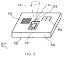
- FIG. 2 is a perspective view showing a configuration of the LD-PD unit 161 in FIG. 1.
- numeral 204 denotes a silicon substrate
- numeral 101 denotes a semiconductor laser that is fixed to the silicon substrate 204
- numerals 193, 194 and 195 denote photodetectors that are formed on the surface of the silicon substrate 204
- numeral 205 denotes an etched mirror that is formed on the silicon substrate 204 and directs the light emitted from the semiconductor laser 101 toward the side above the silicon substrate 204 (emitted light L0).
- the semiconductor laser 101 serving as a light source is fixed directly to the silicon substrate 204.
- the positional relationship between the photodetectors 193, 194 and 195 and the semiconductor laser 101 is stable regardless of temperature variation, vibration and the like. Furthermore, since the semiconductor laser 101 can be surface-mounted, the mounting accuracy is excellent, and mass-production can be achieved easily. Incidentally, the similar effects can be obtained by replacing the etched mirror 205 with a mirror fixed to the silicon substrate 204.
- FIG. 3 is a sectional view showing the structure of the diffraction optical system 118.
- the diffraction optical system 118 includes a polarization anisotropic hologram element 181 and a polarization anisotropic hologram element 182, which are fixed in a predetermined positional relationship.
- Numeral 410 denotes an isotropic substrate whose surface is provided with periodic sawtooth grooves. These sawtooth grooves are filled with a birefringent material 450.
- the isotropic substrate 410 and the birefringent material 450 are selected so that their refractive indexes in the x-axis direction of FIG. 1 match, and do not diffract light polarized in this direction.
- the polarization anisotropic hologram element 181 diffracts light polarized in the y-axis direction of FIG. 1 at maximal efficiency.
- the depth of the grooves is determined according to a birefringence amount of the birefringent material 450 so that light that has passed through the deepest portion of the groove and light that has passed through the shallowest portion thereof have a phase difference of 2 ⁇ .
- incident light L0a polarized in the y-axis direction is converted to light polarized in the y-axis direction L0b by the polarization anisotropic hologram element 181.
- Numeral 411 denotes an isotropic substrate whose surface is provided with grooves formed of periodic protrusions and depressions. These protrusion/ depression grooves are filled with a birefringent material 451.
- the isotropic substrate 411 and the birefringent material 451 are selected so that their refractive indexes in the x-axis direction of FIG. 1 match, and do not diffract light polarized in this direction.
- the depth of the protrusion/ depression grooves is determined according to a birefringence amount of the birefringent material 451 so as to diffract light polarized in the y-axis direction of FIG. 1 at predetermined diffraction efficiency and transmittance.
- ⁇ (2/ ⁇ ) 2 ⁇ sin 2 ((4 ⁇ / ⁇ ) ⁇ n ⁇ d ) wherein d is the depth of the groove, ⁇ n is a difference in the refractive indexes with respect to light polarized in the y-axis direction between the isotropic substrate 411 and the birefringent material 451, and ⁇ is a wavelength of the light source.
- the diffraction optical system 118 that bends the traveling direction of the incident light and diffracts a part of this light can be realized.
- the grooves formed on the isotropic substrate 410 and those formed on the isotropic substrate 411 are illustrated in the same direction (the direction toward the back of the sheet) in FIG. 3 for convenience, they are formed in different directions in practice. In other words, adjustment is made so that the +1-order diffraction light (L1), the -1-order diffraction light (L2) and the transmitted light (L3) enter suitably the photodetectors 193, 194 and 195 on the LD-PD unit 161 in FIG. 2, respectively.
- the isotropic substrate is not limited to a substrate formed of a single material but may be one obtained by forming or bonding a transparent material of a different type onto a substrate transparent to a used wavelength. A similar effect can be obtained by using a birefringent substrate and filling it with an isotropic material. Furthermore, it may be possible to use one obtained by forming a birefringent material on the surface of an isotropic substrate instead of the birefringent substrate.
- the 1/4 wave plate 115 also may be formed as one piece with the surface of the polarization anisotropic hologram element 181 or the polarization anisotropic hologram element 182 that is facing away from the other, thereby simplifying the optical system.
- a linearly polarized light beam L0 emitted from the LD-PD unit 161 is turned into a parallel light beam by the collimator lens 102 and reaches the polarization anisotropic hologram element 181.
- This light beam is not diffracted by the polarization anisotropic hologram element 181 or the polarization anisotropic hologram element 182 because it is polarized in the x-axis direction, and then reaches the 1/4 wave plate 115.
- This light beam further passes through the 1/4 wave plate 115, and is turned into a circularly polarized light beam by an effect of the 1/4 wave plate 115.
- This circularly polarized light beam enters the objective lens 103 and is converged on the optical disk 105 (outgoing path).
- the light beam reflected by the optical disk 105 travels backward along the optical path, passes through the 1/4 wave plate 115 again, becomes linearly polarized light beam whose polarization direction is perpendicular to that of the original light beam (the y-axis direction), and then enters the diffraction optical system 118.
- the diffraction optical system 118 converts the incident light beam into the light whose traveling direction is bent (L3), and the +1-order diffraction light (L1) and -1-order diffraction light (L2), which are obtained by diffracting a part of L3.
- the +1-order diffraction light (L1) and the -1-order diffraction light (L2) respectively enter the photodetector 193 and the photodetector 194 that are arranged on the LD-PD unit 161 shown in FIG. 2 and divided into a plurality of regions, and servo error signals are detected with signals from these regions.
- the light beam L3 that has been transmitted by the polarization anisotropic hologram element 182 is converged to the photodetector 195 that is arranged close to an equivalent light-emitting point along the y-axis direction and then detected as a data signal.
- Such a close arrangement makes it possible to suppress spot shifts owing to error factors such as wavelength variation and reduce a necessary light-receiving area.
- the photodetector 195 is arranged along the y-axis direction because it should be placed at a closest possible position to the light-emitting point. This arrangement is consistent with the need for aligning the photodetectors 193 and 194 in the x-axis direction.
- FIG. 4 is a schematic view showing the polarization anisotropic hologram element 182.
- FIG. 5 is a schematic view showing the shapes of the photodetectors in the LD-PD unit 161 and the position of the light-emitting point.
- the photodetector 193 and the photodetector 194 in the LD-PD unit 161 are arranged on both sides of a light-emitting point (or a point equivalent to a light-emitting point) P.
- the y coordinate at the center of the photodetector 193 corresponds to the y coordinate at the equivalent light-emitting point of the semiconductor laser 101. This arrangement serves to reduce susceptibility to the error factors such as wavelength variation.
- the photodetector 193 is divided into two regions across the y-axis direction, and each of them further is divided into two regions (regions FE1, FE2 and regions FE3, FE4) by a straight line that is parallel to the x-axis. Also, the photodetector 194 is divided into four regions (regions TEa, TEb, TEc, TEd) by straight lines that are parallel to the x-axis and the y-axis, respectively.
- the polarization anisotropic hologram element 182 is divided into large regions A, B, C and D by straight lines that pass the center of this hologram element 182 (the same as the optical axis) and are parallel to the x-axis and the y-axis, respectively. Furthermore, each of the regions is divided into strap-like regions by a plurality of straight lines.
- the returning light that has entered the polarization anisotropic hologram element 182 is converted into the returning +1-order diffraction light L1 and -1-order diffraction light L2 by a diffraction effect of the polarization anisotropic hologram element 182.
- the polarization anisotropic hologram element 182 is divided into a plurality of regions, which are formed so as to diffract light in different directions and wavefronts.
- Each region of the polarization anisotropic hologram element 182 is designed so as to function in the following manner when the smallest light spot is formed on a recording surface of the optical disk 105 (in a focused state).
- the +1-order diffraction light L1 generated from the light that has entered each region of the polarization anisotropic hologram element 182 shown in FIG. 4 reaches each position in the photodetector 193 shown in FIG. 5 as follows.
- the light that has entered the region Ab reaches the position indicated by L1Ab in the photodetector 193 so as to converge on a back side (at the position with a smaller z coordinate) with respect to the photodetector 193.
- the light that has entered the region Af reaches the position indicated by L1Af in the photodetector 193 so as to converge on a front side (at the position with a larger z coordinate) with respect to the photodetector 193.
- the light that has entered the region Bb reaches the position indicated by L1Bb in the photodetector 193 so as to converge on the back side (at the position with a smaller z coordinate) with respect to the photodetector 193.
- the light that has entered the region Bf reaches the position indicated by L1Bf in the photodetector 193 so as to converge on the front side (at the position with a larger z coordinate) with respect to the photodetector 193.
- the light that has entered the region Cb reaches the position indicated by L1Cb in the photodetector 193 so as to converge on the back side (at the position with a smaller z coordinate) with respect to the photodetector 193.
- the light that has entered the region Cf reaches the position indicated by L1Cf in the photodetector 193 so as to converge on the front side (at the position with a larger z coordinate) with respect to the photodetector 193.
- the light that has entered the region Db reaches the position indicated by L1Db in the photodetector 193 so as to converge on the back side (at the position with a smaller z coordinate) with respect to the photodetector 193.
- the light that has entered the region Df reaches the position indicated by L1Df in the photodetector 193 so as to converge on the front side (at the position with a larger z coordinate) with respect to the photodetector 193.
- the -1-order diffraction light L2 that is generated by the polarization anisotropic hologram element 182 enters the following position in the photodetector 194.
- the light that has entered the region Ab in FIG. 4 reaches the position indicated by L2Ab in FIG. 5.
- the light that has entered the region Af reaches the position indicated by L2Af.
- the light that has entered the region Bb reaches the position indicated by L2Bb.
- the light that has entered the region Bf reaches the position indicated by L2Bf.
- the light that has entered the region Cb reaches the position indicated by L2Cb.
- the light that has entered the region Cf reaches the position indicated by L2Cf.
- the light that has entered the region Db reaches the position indicated by L2Db.
- the light that has entered the region Df reaches the position indicated by L2Df.
- An optical head device with the above-described configuration can detect various signals in the following manner.
- a tracking error signal is detected by the photodetector 194.
- one of two methods is used suitably depending on the type of the optical disk 105.
- a push-pull method is used for an optical disk with a continuous groove (for example, a recording/ reproducing optical disk)
- a phase difference method is used for an optical disk with pit-shaped track information (for example, a ROM disk).
- the tracking error signal TE according to the phase difference method can be obtained by phase comparison of (TEa + TEc) and (TEb + TEd).
- a focus error signal FE is detected by the photodetector 193.
- the FE signal has an offset owing to a spot shift accompanied with a change in emission wavelength of the semiconductor laser 101.
- the data signal is detected only with a signal from the photodetector 195.
- the light (L3) for detecting the data signal converges onto the photodetector 195, and its spot is smaller than that of the light (L1, L2) for detecting the servo error signals.
- the light-receiving area in the photodetector 195 can be reduced, resulting in a smaller capacitance of the photodetector. Consequently, it is possible to achieve excellent frequency characteristics, so that the data signal can be reproduced at a high speed.
- the optical head device since the light-receiving area is small, the optical head device is not easily affected by stray light. Thus, even in a system with much stray light (for example, a system for reproducing information from an optical disk with many layers in which the information is recorded), an excellent reproduction signal can be obtained.
- the LD-PD unit 161 can be replaced with an LD-PD unit 162 with a configuration shown in FIG. 6.
- the silicon substrate 204 has a surface provided with the photodetectors 193, 194 and 195 and is fixed onto the upper surface of a holder 301 so that a normal vector of that surface corresponds to the z-axis direction.
- the semiconductor laser 101 On one lateral surface of the holder 301 that is perpendicular to the upper surface, the semiconductor laser 101 further is fixed so that the direction of the emitted light L0 corresponds to the z-axis direction.
- the light-emitting point of the semiconductor laser 101 and the optical axis (the z-axis direction) of the photodetector 195 are positioned far apart. Accordingly, if the diffraction optical system 118 described in the first embodiment is used as it is, the light L3 does not converge onto the photodetector 195.
- the diffraction optical system 118 of FIG. 1 is allowed to have a lens effect in addition to the effect of bending the traveling direction of the incident light.
- This can be achieved by adopting a polarization anisotropic hologram element 181 that has a lens effect in the diffraction optical system 118 with the structure described in FIG. 3.
- a polarization anisotropic hologram element 181 that has a lens effect in the diffraction optical system 118 with the structure described in FIG. 3.
- an LD-PD unit whose light emitting point and optical axis of the photodetector are apart such as the LD-PD unit 162
- the present embodiment is directed to the case where the semiconductor laser 101 and the silicon substrate 204 are fixed directly to the holder 301. However, they do not have to be fixed directly, but may be fixed via a parallel plate such as a silicon substrate as long as they are fixed substantially.
- the LD-PD unit 161 can be replaced with an LD-PD unit 163 with a configuration shown in FIG. 7.
- the silicon substrate 204 has a surface provided with the photodetectors 193, 194 and 195 and is fixed to a holder 302.
- the semiconductor laser 101 is fixed to a silicon substrate 221 on which the etched mirror 205 is formed.
- the silicon substrate 221 further is fixed to the holder 302 so that the direction of the emitted light L0 corresponds to the z-axis direction. Even in the LD-PD unit 163 described above, it is possible to achieve an optical head device with effects similar to those in the first embodiment.
- the LD-PD unit 161 can be replaced with an LD-PD unit 164 with a configuration shown in FIG. 8.
- the silicon substrate 204 has a surface provided with the photodetectors 193, 194 and 195 and is fixed to a holder 303.
- Numeral 117 denotes a surface emitting laser, which is fixed so that the direction of the emitted light L0 corresponds to the z-axis direction.
- the diffraction optical system 118 shown in FIG. 1 also can be constituted using a blazed hologram that has a shape approximating that of the polarization anisotropic hologram element 181 shown in FIG. 3 in the first embodiment.
- FIG. 9 is a structural view showing a diffraction optical system according to the fifth embodiment.
- the hologram element 182 is the same as that in FIG. 3.
- a polarization anisotropic hologram element 183 is obtained by changing the groove shape of the polarization anisotropic hologram element 181 of FIG. 3 from the sawtooth shape into a step-like shape.
- an isotropic substrate 412 and a birefringent material 452 are selected so that their refractive indexes in the x-axis direction of FIG. 1 match, and do not diffract light polarized in this direction.
- N the number of steps
- the polarization anisotropic hologram element 183 can be produced by a production process widely used for manufacturing semiconductors (for example, photolithography), and this makes mass production easy.
- the diffraction efficiency is lower than that of the polarization anisotropic hologram element 181 used in the first embodiment, there is no practical problem if the value of N is set to be large as necessary.
- the number N of steps on the surface is set to be the mth power of 2 where m is an integer (2 m )
- m is an integer (2 m )
- grooves formed on the polarization anisotropic hologram element 182 and those formed on the polarization anisotropic hologram element 183 are illustrated in the same direction (the direction toward the back of the sheet) in FIG. 9 for convenience, they are formed in different directions in practice.
- the 1/4 wave plate 115 also may be formed as one piece with the surface of the polarization anisotropic hologram element 183 or 182 that is facing away from the other, thereby simplifying the optical system.
- the diffraction optical system 118 shown in FIG. 1 also can be constituted using a polarization anisotropic hologram element 184 shown in FIG. 10.
- Numerals 412 and 413 denote isotropic substrates having the same refractive index.
- the surface of the isotropic substrate 412 is provided with sawtooth grooves, while that of the isotropic substrate 413 is provided with grooves formed of protrusions and depressions.
- the isotropic substrates 412 and 413 are arranged so that their grooves face each other, between which a birefringent material 453 is filled.
- the birefringent material 453 is selected so as to match its refractive index to the refractive indexes of the isotropic substrates 412 and 413 with respect to the x-axis direction of FIG. 1. This achieves an effect that light polarized in this direction is not diffracted.
- the depth of the grooves of the isotropic substrate 412 is determined according to a birefringence amount of the birefringent material 453 so that light that has passed through the deepest portion of the groove and light that has passed through the shallowest portion thereof have a phase difference of 2 ⁇ .
- the groove depth of the isotropic substrate 413 is determined as described in the first embodiment, for achieving a predetermined diffraction efficiency.
- the present embodiment makes it possible to achieve a polarization anisotropic hologram element that is applicable to the diffraction optical system 118.
- the grooves formed on the isotropic substrate 412 and those formed on the isotropic substrate 413 are illustrated in the same direction (the direction toward the back of the sheet) in FIG. 10 for convenience, they are formed in different directions in practice.
- the 1/4 wave plate 115 also may be formed as one piece with the surface of the polarization anisotropic hologram element 184, thereby simplifying the optical system.
- the diffraction optical system 118 shown in FIG. 1 also can be constituted using a polarization anisotropic hologram element 185 shown in FIG. 11.
- the polarization anisotropic hologram element 185 is obtained by replacing the isotropic substrate 412 of the polarization anisotropic hologram element 184 shown in FIG. 10 with an isotropic substrate 414 having a step-like surface shape.
- this polarization anisotropic hologram element can be produced by a production process widely used for manufacturing semiconductors (for example, photolithography), and this makes mass production easy. Also in the present embodiment, when the number N of steps on the surface is set to be the m th power of 2 where m is an integer (2 m ), it is possible to produce the hologram element 185 by m etching processes, thereby realizing a hologram element having an excellent diffraction efficiency with fewer production processes.
- the grooves formed on the isotropic substrate 413 and those formed on the isotropic substrate 414 are illustrated in the same direction (the direction toward the back of the sheet) in FIG. 11 for convenience, they are formed in different directions in practice.
- the 1/4 wave plate 115 also may be formed as one piece with the surface of the polarization anisotropic hologram element 185, thereby simplifying the optical system.
- the present embodiment makes it possible to achieve a polarization anisotropic hologram element that is applicable to the diffraction optical system 118.
- FIG. 12A is a perspective view showing the isotropic substrate 412 used in the sixth embodiment
- FIG. 12B is a perspective view showing the isotropic substrate 413 used in the sixth embodiment
- FIG. 12C is a perspective view showing an isotropic substrate 415 used in the eighth embodiment.
- FIG. 13 illustrates a structure of a polarization anisotropic hologram element 186 based on the present embodiment.
- the isotropic substrate 415 shown in FIG. 12C is filled with the birefringent material 453 used in the sixth embodiment, thus forming the diffraction optical system 118.
- the polarization anisotropic hologram element 186 can generate diffraction light L3 as well as diffraction light L1 and its complex conjugate wave, i.e., diffraction light L2.
- the diffraction light L1 and the diffraction light L2 are not higher order diffraction lights accompanied with the diffraction light L3, but diffraction lights independent of the diffraction light L3.
- the present embodiment makes it possible to achieve an optical system with a simpler structure and a lower cost compared with those of the sixth and seventh embodiments.
- the same effects also can be obtained in the case of replacing the isotropic substrate 412 with the isotropic substrate 414 used in the seventh embodiment.
- the 1/4 wave plate 115 also may be formed as one piece with the surface of the polarization anisotropic hologram element 186, thereby simplifying the optical system.
- FIG. 14A is a perspective view showing the isotropic substrate 414 shown in FIG. 11 used in the seventh embodiment
- FIG. 14B is a perspective view showing the isotropic substrate 413 used in the seventh embodiment
- FIG. 14C is a perspective view showing an isotropic substrate 416 used in the ninth embodiment.
- the shape function d 1 (x, y) of the isotropic substrate 414 and the shape function d 2 (x, y) of the isotropic substrate 413 are determined as described in the seventh embodiment, while the shape function d 0 (x, y) of the isotropic substrate 416 is determined as a composite of d 1 (x, y) and d 2 (x, y).
- d 0 (x, y) mod(d 1 (x, y) + d2(x, y), ⁇ / ⁇ n ), wherein mod(A, B) is defined as a function representing the remainder obtained by dividing A by B, ⁇ n is a difference in the refractive indexes with respect to light polarized in the y-axis direction between the isotropic substrate 416 and the birefringent material 453, and ⁇ is a wavelength of the light source.
- FIG. 15 illustrates a structure of a polarization anisotropic hologram element 187 based on the present embodiment.
- This hologram element is formed by filling the isotropic substrate 416 shown in FIG. 14C with the birefringent material 453.
- the present embodiment can constitute a polarization anisotropic hologram element by a substrate with shallower grooves than that in the eighth embodiment, allowing easier production.
- a polarization anisotropic hologram element can be produced with simpler processes by selecting the shape functions d 1 and d 2 suitably.
- the groove depth according to the shape function d 2 is set to be the depth of one step according to the shape function d 1
- the surface shape according to the shape function do has the equal number N of steps to the surface shape according to the shape function d 1 , so that the isotropic substrate 416 can be produced by the same process as for the isotropic substrate 414.
- the present embodiment makes it possible to achieve a polarization anisotropic hologram element that is applicable to the diffraction optical system 118 and produced by simple processes.
- the 1/4 wave plate 115 also may be formed as one piece with the surface of the polarization anisotropic hologram element 187, thereby simplifying the optical system.
- An optical head device is constituted using a photodetector 196 shown in FIG. 16 instead of the photodetector 195 on the LD-PD unit 161 shown in FIG. 2 of the optical head device according to the first embodiment.
- the photodetector 196 has two regions (RF1, RF2).
- the groove shapes of polarization anisotropic hologram elements 188 and 189 shown in FIGs. 17 and 18, which correspond to the polarization anisotropic hologram elements 181 and 182 in FIG. 3, are determined in the following manner.
- the polarization anisotropic hologram element 188 has two regions (region L, region R) that have different groove shapes.
- the two regions are both designed so as to diffract light polarized in the y-axis direction at maximal efficiency, like the polarization anisotropic hologram element 181.
- the groove shape in the region L is determined so that incident light polarized in the y-axis direction is converted to diffraction light reaching RF1 of the photodetector 196.
- the groove shape in the region R is determined so that incident light polarized in the y-axis direction is converted to diffraction light reaching RF2 of the photodetector 196.
- the polarization anisotropic hologram element 189 shown in FIG. 18 is divided as in the polarization anisotropic hologram element 182 shown in FIG. 4 in the first embodiment.
- Each region of the polarization anisotropic hologram element 189 is designed so as to function in the following manner when the smallest light spot is formed on a recording surface of the optical disk 105 (in a focused state).
- the light that has been diffracted by the region R (FIG. 17) and entered the region Ab (FIG. 18) reaches the position indicated by L1Ab (FIG. 16) in the photodetector 193 so as to converge on a back side (at the position with a smaller z coordinate) with respect to the photodetector 193.
- the light that has been diffracted by the region R and entered the region Af reaches the position indicated by L1Af in the photodetector 193 so as to converge on a front side (at the position with a larger z coordinate) with respect to the photodetector 193.
- the light that has been diffracted by the region R and entered the region Bb reaches the position indicated by L1Bb in the photodetector 193 so as to converge on the back side (at the position with a smaller z coordinate) with respect to the photodetector 193.
- the light that has been diffracted by the region R and entered the region Bf reaches the position indicated by L1Bf in the photodetector 193 so as to converge on the front side (at the position with a larger z coordinate) with respect to the photodetector 193.
- the light that has been diffracted by the region L and entered the region Cb reaches the position indicated by L1Cb in the photodetector 193 so as to converge on the back side (at the position with a smaller z coordinate) with respect to the photodetector 193.
- the light that has been diffracted by the region L and entered the region Cf reaches the position indicated by L1Cf in the photodetector 193 so as to converge on the front side (at the position with a larger z coordinate) with respect to the photodetector 193.
- the light that has been diffracted by the region L and entered the region Db reaches the position indicated by L1Db in the photodetector 193 so as to converge on the back side (at the position with a smaller z coordinate) with respect to the photodetector 193.
- the light that has been diffracted by the region L and entered the region Df reaches the position indicated by L1Df in the photodetector 193 so as to converge on the front side (at the position with a larger z coordinate) with respect to the photodetector 193.
- the -1-order diffraction light L2 that is generated by the polarization anisotropic hologram element 189 enters the following position in the photodetector 194.
- the light that has entered the region Ab reaches the position indicated by L2Ab.
- the light that has entered the region Af reaches the position indicated by L2Af.
- the light that has entered the region Bb reaches the position indicated by L2Bb.
- the light that has entered the region Bf reaches the position indicated by L2Bf.
- the light that has entered the region Cb reaches the position indicated by L2Cb.
- the light that has entered the region Cf reaches the position indicated by L2Cf.
- the light that has entered the region Db reaches the position indicated by L2Db.
- the light that has entered the region Df reaches the position indicated by L2Df.
- Light L3L and light L3R which have entered the regions L and R respectively in the polarization anisotropic hologram element 188 and been transmitted without being diffracted by the polarization anisotropic hologram element 189, are focused on light-receiving regions RF1 and RF2 respectively in the photodetector 196.
- the optical head device can detect signals even in a system in which an information signal such as an address is recorded by positions on the right and left of a groove.
- the present embodiment is directed to the case of modifying a detection region of the LD-PD unit 161 used in the first embodiment, there is no particular limitation as long as the light-receiving elements and the light-emitting element are arranged close to each other and two light beams for data signals can be detected.
- FIG. 19 illustrates an optical information processing apparatus according to the eleventh embodiment of the present invention.
- the present embodiment will be directed to the optical information processing apparatus using the optical head device of the first embodiment, but it also is possible to constitute an optical information processing apparatus in a similar manner using the optical head devices of the other embodiments.
- the optical disk 105 is rotated by an optical disk rotating mechanism 501.
- An optical head device 500 is driven to a track having desired information in the optical disk 105 by an optical head device driving device 502.
- Signals detected from the light-receiving regions of the optical head device 500 are current/ voltage converted and amplified by a head amplifier 503, then input to an electric circuit 504.
- the electric circuit 504 calculates the input signals to obtain a servo error signal, and then transmits to the optical head device 500 a signal for moving the objective lens slightly. With this signal, the optical head device 500 performs a focus servo and a tracking servo with respect to the optical disk 105 and reads out, writes in or erase a data signal with respect to the optical disk 105.
- FIG. 20 is a circuit diagram showing the head amplifier 503 and a part of the electric circuit 504.
- a data signal from the photodetector 195 is current/ voltage converted by a circuit IV RF . Since a servo error signal need not be detected from this signal, a circuit configuration with a limited bandwidth can be used, making it easier to achieve a circuit having a simple configuration and low noise level. Conventionally, since the data signal was obtained by totaling all the signals from the amplifiers in 6 channels, an amplifier noise was added in as well. On the other hand, since an amplifier noise of only 1 channel is mixed in according to the present invention, it is possible to suppress the noise down to 1/6 0.5 of the conventional level. When using the optical head device illustrated in the tenth embodiment, it is appropriate to add one more circuit that is similar to the circuit IV RF .
- FE1 and FE3 on the one hand and FE2 and FE4 on the other hand are connected, and the former is current/ voltage converted by a circuit IV 1 and the latter is current/ voltage converted by a circuit IV 2 , thus obtaining the focus error signal from the difference in their outputs.
- the amplifier used in this circuit system does not detect the data signal, it may be operated in a servo bandwidth at relatively low frequencies, thus achieving a low-current amplifier with a simple configuration.
- signals from the regions (TEa, TEb, TEc, TEd) in the photodetector 194 are current/voltage converted by circuits TV a , IV b , IV c , IV d , respectively.
- the used frequency band of the amplifier varies depending on the detection method of the servo error signal.
- a servo frequency band alone is suitable for detecting only a push-pull signal, while a signal frequency band alone is suitable for detecting only a phase difference signal.
- the circuits may be simple.
- the description of the present embodiment is directed to the case of providing the head amplifier 503 and a part of the electric circuit 504 independently of the optical head device, there is no particular limitation to this. It also may be possible to mount all or a part of them inside the optical head device 500 or to provide them on the substrate of the light-receiving element.
Abstract
Description
- The present invention relates to an optical head device, an optical information processing apparatus and an optical element for recording/reproducing or erasing information that is stored in an optical medium such as an optical disk or an optical card.
- With the development of optical disks in recent years, the variety of optical disks in use such as recording and reproducing optical disks and read-only memory (ROM) optical disks has been increasing. Under such circumstances, an optical head device that can reproduce information from these plural types of optical disks has been devised.
- In the following, a conventional technology will be described with reference to FIG. 21. In FIG. 21,
numeral 160 denotes an LD-PD (Laser Diode Photo Detector) unit that is arranged so as to emit light polarized in an x-axis direction. The LD-PD unit 160, which will be described more specifically later, has photodetectors for detecting light containing a signal and a semiconductor laser serving as a light source that are fixed in a certain positional relationship.Numeral 102 denotes a collimator lens. Numeral 180 denotes a polarization anisotropic hologram having a function of transmitting light polarized in a certain direction and diffracting light polarized in a direction perpendicular thereto, which is arranged so as to transmit light polarized in the x-axis direction. Numeral 115 denotes a 1/4 wave plate, andnumeral 103 denotes an objective lens. Numeral 106 denotes a holder for maintaining the positional relationship between the polarizationanisotropic hologram 180, the 1/4wave plate 115 and theobjective lens 103. Numeral 105 denotes an optical disk that is arranged so that its tangential direction corresponds to a y-axis direction. Numeral 112 denotes a driving member for driving theholder 106. - The following is an explanation of its operation. A linearly polarized light beam L0 emitted from a radiation light source in the LD-
PD unit 160 is not diffracted by the polarizationanisotropic hologram 180 because it is polarized in the x-axis direction, and then reaches the 1/4wave plate 115. This light beam further passes through the 1/4wave plate 115, becomes circularly polarized by an effect of the 1/4wave plate 115, enters theobjective lens 103 and is converged on the optical disk 105 (outgoing path). - The light beam reflected by the
optical disk 105 travels backward along the optical path, passes through the 1/4wave plate 115 again, becomes linearly polarized light beam whose polarization direction is perpendicular to that of the original light beam (the y-axis direction), and then enters the polarizationanisotropic hologram 180. Returning +1-order diffraction light L1 and -1-order diffraction light L2 that are generated from the polarizationanisotropic hologram 180 reach photodetectors arranged in the LD-PD unit 160 where a servo error signal and a recorded information signal are detected. - The following is a detailed description of how the signals are detected, with reference to FIGs. 22 and 23. FIG. 22 is a schematic view showing the polarization
anisotropic hologram 180, and FIG. 23 is a schematic view showing the LD-PD unit 160. - As shown in FIG. 22, the polarization
anisotropic hologram 180 is divided into large regions A, B, C and D by straight lines that pass through the center of the polarization anisotropic hologram 180 (the same as an optical axis) and are parallel to the x-axis and the y-axis, respectively. Furthermore, each of the regions is divided into small strap-like regions by a plurality of straight lines. Within one large region, hologram patterns with the same functions are formed in every other small strap-like regions. Hereinafter, the regions having the same hologram patterns are altogether referred to as one small region (region Ab, Af, Bb, Bf, Cb, Cf, Db, Df). - As shown in FIG. 23, the LD-
PD unit 160 has aphotodetector 191 and aphotodetector 192, which are arranged on both sides of a light-emitting point (or a point equivalent to a light-emitting point) P. Thephotodetector 191 is divided into two regions across the y-axis direction, and each of them further is divided into two regions by a straight line that is parallel to the x-axis, thus forming regions FE1, FE2 and regions FE3, FE4. Also, thephotodetector 192 is divided into four regions (regions TEa, TEb, TEc, TEd) by straight lines that are parallel to the x-axis and the y-axis, respectively. - The returning light that has entered the polarization
anisotropic hologram 180 is converted into the returning +1-order diffraction light L1 and - 1-order diffraction light L2 by a diffraction effect of the polarizationanisotropic hologram 180. - As described above, the polarization
anisotropic hologram 180 is divided into a plurality of regions, which are formed so as to diffract light in different directions and wavefronts. Each region of the polarizationanisotropic hologram 180 is designed so as to function in the following manner when the smallest light spot is formed on a recording surface of the optical disk 105 (in a focused state). - The +1-order diffraction light L1 generated from the light that has entered each region of the polarization
anisotropic hologram 180 shown in FIG. 22 reaches each position in thephotodetector 191 shown in FIG. 23 as follows. - The light that has entered the region Ab reaches the position indicated by L1Ab in the
photodetector 191 so as to converge on a back side (at the position with a smaller z coordinate) with respect to thephotodetector 191. The light that has entered the region Af reaches the position indicated by L1Af in thephotodetector 191 so as to converge on a front side (at the position with a larger z coordinate) with respect to thephotodetector 191. - The light that has entered the region Bb reaches the position indicated by L1Bb in the
photodetector 191 so as to converge on the back side (at the position with a smaller z coordinate) with respect to thephotodetector 191. The light that has entered the region Bf reaches the position indicated by L1Bf in thephotodetector 191 so as to converge on the front side (at the position with a larger z coordinate) with respect to thephotodetector 191. - The light that has entered the region Cb reaches the position indicated by L1Cb in the
photodetector 191 so as to converge on the back side (at the position with a smaller z coordinate) with respect to thephotodetector 191. The light that has entered the region Cf reaches the position indicated by L1Cf in thephotodetector 191 so as to converge on the front side (at the position with a larger z coordinate) with respect to thephotodetector 191. - The light that has entered the region Db reaches the position indicated by L1Db in the
photodetector 191 so as to converge on the back side (at the position with a smaller z coordinate) with respect to thephotodetector 191. The light that has entered the region Df reaches the position indicated by L1Df in thephotodetector 191 so as to converge on the front side (at the position with a larger z coordinate) with respect to thephotodetector 191. - Next, the -1-order diffraction light L2 that is generated by the polarization
anisotropic hologram 180 enters thephotodetector 192 as follows. - The light that has entered the region Ab in FIG. 22 reaches the position indicated by L2Ab in FIG. 23. The light that has entered the region Af reaches the position indicated by L2Af.
- The light that has entered the region Bb reaches the position indicated by L2Bb. The light that has entered the region Bf reaches the position indicated by L2Bf.
- The light that has entered the region Cb reaches the position indicated by L2Cb. The light that has entered the region Cf reaches the position indicated by L2Cf.
- The light that has entered the region Db reaches the position indicated by L2Db. The light that has entered the region Df reaches the position indicated by L2Df.
- An optical head device with the above-described configuration can detect various signals in the following manner. A tracking error signal is detected by the
photodetector 192. When detecting the tracking error signal, one of two methods is used suitably depending on the type of theoptical disk 105. In other words, a push-pull method is used for an optical disk with a continuous groove (for example, a recording/ reproducing optical disk), while a phase difference method is used for an optical disk with pit-shaped track information (for example, a ROM disk). - When a signal output from each region of the
photodetector 192 is expressed by the name of this region, a tracking error signal TE according to the push-pull method can be obtained by - A focus error signal FE is detected by the
photodetector 191. When a signal output from each region of thephotodetector 191 is expressed by the name of this region, the focus error signal FE can be obtained by - A data signal S can be obtained by totaling signals from the
photodetector 191 and thephotodetector 192, i.e., - In the optical head device with the conventional configuration described above, the data signal S has been detected by the sum of servo error signals (the focus error signal FE and the tracking error signal TE). Since the photodetector for detecting the servo error signals has to detect incident light in a defocused state, it has been necessary for the photodetector to have a large light-receiving area. An increase in the light-receiving area results in a larger capacitance of the photodetector. Consequently, the frequency characteristics of a detected signal deteriorate, leading to a problem that the data signal cannot be reproduced at a high speed.
- Moreover, since the light-receiving area is large, the optical head device easily is affected by stray light. Thus, in a system with much stray light, for example, a system for reproducing information from an optical disk with many layers in which the information is recorded, a signal to noise ratio (S/N) deteriorates, causing a problem that an excellent reproduction signal cannot be obtained.
- It is an object of the present invention to solve the conventional problems described above and to provide an optical head device in which a light-receiving area of a light-receiving element for detecting a data signal can be reduced, thereby achieving improved fast response characteristics and reduced susceptibility to stray light. It is a further object of the present invention to provide an optical element that is suitable for realizing such an optical head device. Furthermore, it is an object of the present invention to provide an optical information processing apparatus in which the number of head amplifiers necessary for detecting a data signal can be reduced, thereby obtaining a data signal with reduced amplifier noise.
- In order to achieve the above-mentioned objects, the present invention has the following configuration.
- An optical head device with a first basic configuration according to the present invention includes a radiation light source, a converging optical system for converging a light beam from the radiation light source onto an information medium and forming a minute spot, a photodetector, divided into a plurality of regions, for receiving the light beam reflected by the information medium and outputting a photoelectric current, and a diffraction optical system for diffracting the light beam reflected by the information medium as a diffraction light beam and directing it to the photodetector.
The diffraction optical system generates a first diffraction light beam and a second diffraction light beam from an incident light beam in a predetermined energy distribution ratio. The first diffraction light beam enters a first detection region in the photodetector, and the second diffraction light beam is not a complex conjugate wave of the first diffraction light beam. Information recorded on the information medium is read out using the first diffraction light beam alone, while a servo error signal is obtained using the second diffraction light beam. - An optical head device with a second basic configuration according to the present invention includes a radiation light source, a converging optical system for converging a light beam from the radiation light source onto an information medium and forming a minute spot, a photodetector, divided into a plurality of regions, for receiving the light beam reflected by the information medium and outputting a photoelectric current, and a diffraction optical system for diffracting the light beam reflected by the information medium as a diffraction light beam and directing it to the photodetector. The diffraction optical system includes a first diffraction region and a second diffraction region. The first diffraction region generates a first diffraction light beam and a second diffraction light beam from an incident light beam in a predetermined energy distribution ratio. The first diffraction light beam enters a first detection region in the photodetector, and the second diffraction light beam is not a complex conjugate wave of the first diffraction light beam. The second diffraction region generates a third diffraction light beam and a fourth diffraction light beam from an incident light beam in a predetermined energy distribution ratio. The third diffraction light beam enters a second detection region in the photodetector and the fourth diffraction light beam is not a complex conjugate wave of the third diffraction light beam.
Information recorded on the information medium is read out using the first diffraction light beam and the third diffraction light beam alone, while a servo error signal is obtained using the second diffraction light beam and the fourth diffraction light beam. - In accordance with the first and second optical head devices described above, the information recorded on the information medium is read out using the diffraction light beam that is different from the diffraction light beam for obtaining the servo error signal. Thus, it is possible to provide a photodetection region exclusively for reading out the information recorded on the information medium, thus achieving a smaller area of the photodetection region. As a result, an optical head device having excellent frequency characteristics and allowing a high-speed reproduction of a data signal can be achieved. Furthermore, it is not easily affected by stray light, and thus can obtain an excellent reproduction signal even in a system with much stray light (for example, a system for reproducing information from an optical disk with many layers in which the information is recorded).
- In the optical head device with any of the basic configurations described above, it is preferable that the radiation light source and the photodetector are arranged and fixed close to each other.
- In this configuration, a reflection mirror further may be provided for reflecting the light beam from the radiation light source substantially perpendicularly to a surface of the photodetector.
- Alternatively, it is possible to provide further a rigid body including a first surface and a second surface that are substantially perpendicular to each other, so that the radiation light source is fixed substantially to the first surface, and the photodetector is fixed substantially to the second surface.
- Alternatively, the radiation light source can be fixed to a surface of a holding member, a reflection mirror for reflecting the light beam from the radiation light source substantially perpendicularly to the surface of the holding member can be formed or disposed on the holding member, and the holding member and the photodetector can be fixed substantially to a single surface of a single rigid body.
- Alternatively, the radiation light source can be a surface emitting laser, and the radiation light source and the photodetector can be fixed substantially to a single surface of a single rigid body.
- In the optical head device with any of the configurations described above, the region for photodetection for reading out the information recorded on the information medium can be arranged close to a light-emitting position of the radiation light source, at a position along a tangential direction of the information medium with respect to the light-emitting position.
- In the optical head device with any of the configurations described above, the region for photodetection for detecting a focus error signal can be divided into a plurality of regions by a straight line in a radial direction of the information medium.
- In this case, the plurality of regions for detecting the focus error signal can be arranged away from each other, at positions along the radial direction of the recording medium with respect to a light-emitting position of the radiation light source.
- In the optical head device with any of the configurations described above, the diffraction light beam for reading out the information recorded on the information medium can be converged to the region for photodetection for reading out the information recorded on the information medium.
- In the optical head device with any of the configurations described above, the diffraction optical system can generate both a +1-order diffraction light beam and a -1-order diffraction light beam for detecting the servo error signal. In the optical head device with this configuration, a focus error signal can be detected with the +1-order diffraction light beam, and a tracking error signal can be detected with the -1-order diffraction light beam.
- An optical element with a basic structure according to the present invention transmits a light beam polarized in a first direction and diffracts a light beam polarized in a second direction that is perpendicular to the first direction. The optical element diffracts an incident light beam polarized in the second direction as a first diffraction light beam including no complex conjugate wave at a predetermined efficiency, and generates a diffraction light beam whose wavefront is different from that of a higher order diffraction light beam of the first diffraction light beam.
- By using this optical element, the above-described optical head device of the present invention can be realized easily.
- It is preferable that the diffraction optical system in the optical head device with any of the configurations described above includes this optical element with the basic structure.
- The optical element with the basic structure described above preferably has a first diffraction element for transmitting the light beam polarized in the first direction and diffracting all the light beam polarized in the second direction, and a second diffraction element for transmitting the light beam polarized in the first direction and diffracting the light beam polarized in the second direction at a predetermined efficiency. The first diffraction element includes a first light-transmitting material and a second light-transmitting material. A refractive index of the first light-transmitting material and a refractive index of the second light-transmitting material are equal for the light beam polarized in the first direction and different for the light beam polarized in the second direction. An interface between the first light-transmitting material and the second light-transmitting material has a sawtooth groove shape. The second diffraction element includes a third light-transmitting material and a fourth light-transmitting material. A refractive index of the third light-transmitting material and a refractive index of the fourth light-transmitting material are equal for the light beam polarized in the first direction and different for the light beam polarized in the second direction. An interface between the third light-transmitting material and the fourth light-transmitting material has a groove shape formed of periodic protrusions and depressions. The first diffraction element and the second diffraction element are fixed to each other in a predetermined relative positional relationship.
- Also, the optical element with the basic structure described above preferably has a first diffraction element for transmitting the light beam polarized in the first direction and diffracting all the light beam polarized in the second direction, and a second diffraction element for transmitting the light beam polarized in the first direction and diffracting the light beam polarized in the second direction at a predetermined efficiency. The first diffraction element includes a first light-transmitting material and a second light-transmitting material. A refractive index of the first light-transmitting material and a refractive index of the second light-transmitting material are equal for the light beam polarized in the first direction and different for the light beam polarized in the second direction. An interface between the first light-transmitting material and the second light-transmitting material has a step-like shape. The second diffraction element includes a third light-transmitting material and a fourth light-transmitting material. A refractive index of the third light-transmitting material and a refractive index of the fourth light-transmitting material are equal for the light beam polarized in the first direction and different for the light beam polarized in the second direction. An interface between the third light-transmitting material and the fourth light-transmitting material has a groove shape formed of periodic protrusions and depressions. The first diffraction element and the second diffraction element are fixed to each other in a predetermined relative positional relationship.
- Furthermore, the optical element with the basic structure described above preferably includes a first light-transmitting material, a second light-transmitting material and a third light-transmitting material. The first light-transmitting material and the second light-transmitting material are adjacent to each other via a first interface, and the second light-transmitting material and the third light-transmitting material are adjacent to each other via a second interface. A refractive index of the first light-transmitting material and a refractive index of the second light-transmitting material are equal for the light beam polarized in the first direction and different for the light beam polarized in the second direction. The refractive index of the second light-transmitting material and a refractive index of the third light-transmitting material are equal for the light beam polarized in the first direction and different for the light beam polarized in the second direction. The first interface has a sawtooth groove shape, and the second interface has a groove shape formed of periodic protrusions and depressions.
- Furthermore, the optical element with the basic structure described above preferably includes a first light-transmitting material; a second light-transmitting material and a third light-transmitting material. The first light-transmitting material and the second light-transmitting material are adjacent to each other via a first interface, and the second light-transmitting material and the third light-transmitting material are adjacent to each other via a second interface. A refractive index of the first light-transmitting material and a refractive index of the second light-transmitting material are equal for the light beam polarized in the first direction and different for the light beam polarized in the second direction. The refractive index of the second light-transmitting material and a refractive index of the third light-transmitting material are equal for the light beam polarized in the first direction and different for the light beam polarized in the second direction. The first interface has a step-like shape, and the second interface has a groove shape formed of periodic protrusions and depressions.
- Furthermore, the optical element with the basic structure described above preferably includes a first light-transmitting material and a second light-transmitting material. The first light-transmitting material and the second light-transmitting material are adjacent to each other via an interface. A refractive index of the first light-transmitting material and a refractive index of the second light-transmitting material are equal for the light beam polarized in the first direction and different for the light beam polarized in the second direction. A shape of the interface is defined by a shape function expressed by a sum of a function d1 representing a sawtooth groove shape or a step-like shape and a function d2 representing a groove shape formed of periodic protrusions and depressions.
- Furthermore, the optical element with the basic structure described above preferably includes a first light-transmitting material and a second light-transmitting material. The first light-transmitting material and the second light-transmitting material are adjacent to each other via an interface. A refractive index of the first light-transmitting material and a refractive index of the second light-transmitting material are equal for the light beam polarized in the first direction and different by Δn for the light beam polarized in the second direction. When λ is a wavelength of the incident light, a shape of the interface is defined by a shape function expressed by a remainder obtained when dividing by λ/Δn a sum of a function d1 representing a sawtooth groove shape or a step-like shape and a function d2 representing a groove shape formed of periodic protrusions and depressions.
- In the optical element with any of the structures described above, it is possible to provide as one piece a wave plate for converting the light beam polarized in the first direction into a circularly polarized light beam.
- In the optical head device with any of the configurations described above, the diffraction optical system can include the optical element with any of the structures describe above.
- An optical information processing apparatus in accordance with the present invention includes the optical head device having any of the above-described configurations, and an electric circuit for processing a signal detected by the optical head device and extracting a desired signal.
- In accordance with this optical information processing apparatus, an optical information processing apparatus having excellent frequency characteristics and allowing a high-speed reproduction of a data signal can be achieved. Furthermore, it is not easily affected by stray light, and thus can obtain an excellent reproduction signal even in a system with much stray light (for example, a system for reproducing information from an optical disk with many layers in which the information is recorded). Moreover, since the number of head amplifiers for reading out the information recorded on the information medium can be reduced, it is possible to simplify a circuit configuration compared with a conventional one, reduce the amplifier noise and achieve an inexpensive system.
- In the optical information processing apparatus with this configuration, the electric circuit can include an electric circuit having a gain only in an information signal frequency band and current/ voltage converting and amplifying an output from the photodetector for detecting an information signal recorded on the information medium.
- In the optical information processing apparatus with any of the configurations described above, the electric circuit can include an electric circuit having a gain only in a servo signal frequency band and current/voltage converting and amplifying an output from the photodetector for detecting a focus error signal.
- In a first configuration for a tracking control in the optical information processing apparatus with any of the configurations described above, the electric circuit includes an electric circuit having a gain only in a servo signal frequency band and current/ voltage converting and amplifying an output from the photodetector for detecting a tracking error signal. In the optical information processing apparatus with this configuration, the tracking error signal can be detected by a push-pull method.
- Further, in a second configuration for the tracking control in the optical information processing apparatus with any of the configurations described above, the electric circuit includes an electric circuit having a gain only in an information signal frequency band and current/ voltage converting and amplifying an output from the photodetector for detecting a tracking error signal. In the optical information processing apparatus with this configuration, the tracking error signal can be detected by a phase difference method.
- Moreover, in a third configuration for the tracking control in the optical information processing apparatus with any of the configurations described above, the electric circuit includes an electric circuit having a gain in an information signal frequency band and a servo signal frequency band and current/ voltage converting and amplifying an output from the photodetector for detecting a tracking error signal. In the optical information processing apparatus with this configuration, the tracking error signal can be detected by switching or combining a phase difference method and a push-pull method.
-
- FIG. 1 is a sectional view showing a schematic configuration of an optical head device according to a first embodiment.
- FIG. 2 is a perspective view showing a configuration of an LD-PD unit in FIG. 1.
- FIG. 3 is a sectional view showing a schematic structure of a diffraction optical system in FIG. 1.
- FIG. 4 is a plan view showing schematically a polarization anisotropic hologram element in FIG. 1.
- FIG. 5 is a plan view showing schematically shapes of light-receiving elements and a position of a light-emitting point in the LD-PD unit shown in FIG. 2.
- FIG. 6 is a perspective view showing a configuration of an LD-PD unit according to a second embodiment.
- FIG. 7 is a perspective view showing a configuration of an LD-PD unit according to a third embodiment.
- FIG. 8 is a perspective view showing a configuration of an LD-PD unit according to a fourth embodiment.
- FIG. 9 is a sectional view showing a schematic structure of a diffraction optical system according to a fifth embodiment.
- FIG. 10 is a sectional view showing schematically a polarization anisotropic hologram element according to a sixth embodiment.
- FIG. 11 is a sectional view showing schematically a polarization anisotropic hologram element according to a seventh embodiment.
- FIGs. 12A, 12B and 12C are perspective views for describing a structure of a polarization anisotropic hologram element according to an eighth embodiment.
- FIG. 13 is a sectional view showing schematically a polarization anisotropic hologram element according to the eighth embodiment.
- FIGs. 14A, 14B and 14C are perspective views for describing a structure of a polarization anisotropic hologram element according to a ninth embodiment.
- FIG. 15 is a sectional view showing schematically a polarization anisotropic hologram element according to the ninth embodiment.
- FIG. 16 is a plan view showing schematically shapes of light-receiving elements and a position of a light-emitting point according to a tenth embodiment.
- FIG. 17 is a plan view showing schematically a polarization anisotropic hologram element according to the tenth embodiment.
- FIG. 18 is a plan view showing schematically a polarization anisotropic hologram element according to the tenth embodiment.
- FIG. 19 is a structural view of an optical information processing apparatus according to an eleventh embodiment.
- FIG. 20 is a circuit diagram showing a partial configuration of head amplifiers and electric circuits according to the eleventh embodiment.
- FIG. 21 is a sectional view showing a schematic configuration of a conventional optical head device.
- FIG. 22 is a plan view showing schematically a conventional polarization anisotropic hologram.
- FIG. 23 is a plan view showing a schematic configuration of a conventional LD-PD unit.
-
- The following is a description of the first embodiment of the present invention, with reference to the accompanying drawings. FIG. 1 is a sectional view showing a schematic configuration of an optical head device according to the first embodiment. Hereinafter, for convenience of description, the xyz coordinate axes are set as shown at the bottom left corner of this figure, with the arrow of each axis pointing forward. The forward direction of the y-axis is toward the back of the sheet. In the following, the coordinate axes of FIG. 1 are common to the other drawings unless otherwise specified.
- In FIG. 1, numeral 161 denotes an LD-PD unit that is arranged so as to emit light L0 polarized in the x-axis direction. The LD-
PD unit 161, which will be described more specifically later, has photodetectors for detecting light containing signals and a semiconductor laser serving as a light source that are fixed in a certain positional relationship. -
Numeral 102 denotes a collimator lens, which turns the light emitted from the LD-PD unit 161 into parallel light.Numeral 118 denotes a diffraction optical system having the following function. First, it transmits light polarized in the x-axis direction. Then, it bends the traveling direction of light polarized in the y-axis direction in a certain direction, so that the light whose traveling direction has been bent generates diffraction light as well as transmitted light (zero-order diffraction light). In other words, the diffractionoptical system 118 has a function of bending the traveling direction of incident light and diffracting a part of this light. Its specific structure will be described later. -
Numeral 115 denotes a 1/4 wave plate, and numeral 103 denotes an objective lens.Numeral 106 denotes a holder for maintaining the positional relationship between the diffractionoptical system 118, the 1/4wave plate 115 and theobjective lens 103.Numeral 105 denotes an optical disk, and numeral 112 denotes a driving member for driving theholder 106. - In FIG. 1, a radial direction of the
optical disk 105 at the position of a light spot formed on theoptical disk 105 corresponds to the x-axis direction, while a tangential direction of a recording track of the optical disk at this position corresponds to the y-axis direction. - Before the operation of this optical head device is explained, the LD-
PD unit 161 and the diffractionoptical system 118 used in this optical head device will be described. - FIG. 2 is a perspective view showing a configuration of the LD-
PD unit 161 in FIG. 1. In FIG. 2, numeral 204 denotes a silicon substrate, numeral 101 denotes a semiconductor laser that is fixed to thesilicon substrate 204, andnumerals silicon substrate 204. Also, numeral 205 denotes an etched mirror that is formed on thesilicon substrate 204 and directs the light emitted from thesemiconductor laser 101 toward the side above the silicon substrate 204 (emitted light L0). In the LD-PD unit 161 with such a configuration, thesemiconductor laser 101 serving as a light source is fixed directly to thesilicon substrate 204. Therefore, the positional relationship between thephotodetectors semiconductor laser 101 is stable regardless of temperature variation, vibration and the like. Furthermore, since thesemiconductor laser 101 can be surface-mounted, the mounting accuracy is excellent, and mass-production can be achieved easily. Incidentally, the similar effects can be obtained by replacing the etchedmirror 205 with a mirror fixed to thesilicon substrate 204. - FIG. 3 is a sectional view showing the structure of the diffraction
optical system 118. The diffractionoptical system 118 includes a polarizationanisotropic hologram element 181 and a polarizationanisotropic hologram element 182, which are fixed in a predetermined positional relationship. - First, the polarization
anisotropic hologram element 181 will be described.Numeral 410 denotes an isotropic substrate whose surface is provided with periodic sawtooth grooves. These sawtooth grooves are filled with abirefringent material 450. Theisotropic substrate 410 and thebirefringent material 450 are selected so that their refractive indexes in the x-axis direction of FIG. 1 match, and do not diffract light polarized in this direction. - Further, the polarization
anisotropic hologram element 181 diffracts light polarized in the y-axis direction of FIG. 1 at maximal efficiency. For this purpose, the depth of the grooves is determined according to a birefringence amount of thebirefringent material 450 so that light that has passed through the deepest portion of the groove and light that has passed through the shallowest portion thereof have a phase difference of 2π. With this structure, incident light L0a polarized in the y-axis direction is converted to light polarized in the y-axis direction L0b by the polarizationanisotropic hologram element 181. - Next, the polarization
anisotropic hologram element 182 will be described.Numeral 411 denotes an isotropic substrate whose surface is provided with grooves formed of periodic protrusions and depressions. These protrusion/ depression grooves are filled with abirefringent material 451. - The
isotropic substrate 411 and thebirefringent material 451 are selected so that their refractive indexes in the x-axis direction of FIG. 1 match, and do not diffract light polarized in this direction. - In addition, the depth of the protrusion/ depression grooves is determined according to a birefringence amount of the
birefringent material 451 so as to diffract light polarized in the y-axis direction of FIG. 1 at predetermined diffraction efficiency and transmittance. When the ratio of the protrusion to the depression composing the grooves is 1 : 1, +1-order diffraction light (L1) and -1-order diffraction light (L2) have the same diffraction efficiency η, which is expressed by the following equation:isotropic substrate 411 and thebirefringent material 451, and λ is a wavelength of the light source. - Further, the efficiency of transmitted light (L3) η0 is expressed by the following equation:
- For example, in the case of Δn = 0.1 and λ = 0.65 µm, it is appropriate to set d = 0.4 µm for obtaining the efficiency of transmitted light η0 = 50%. The diffraction efficiency at this time is 20% for both the +1-order diffraction light (L1) and the -1-order diffraction light (L2). (This efficiency is taken as an example in the following description.)
- In this manner, the diffraction
optical system 118 that bends the traveling direction of the incident light and diffracts a part of this light can be realized. Although the grooves formed on theisotropic substrate 410 and those formed on theisotropic substrate 411 are illustrated in the same direction (the direction toward the back of the sheet) in FIG. 3 for convenience, they are formed in different directions in practice. In other words, adjustment is made so that the +1-order diffraction light (L1), the -1-order diffraction light (L2) and the transmitted light (L3) enter suitably thephotodetectors PD unit 161 in FIG. 2, respectively. - The isotropic substrate is not limited to a substrate formed of a single material but may be one obtained by forming or bonding a transparent material of a different type onto a substrate transparent to a used wavelength. A similar effect can be obtained by using a birefringent substrate and filling it with an isotropic material. Furthermore, it may be possible to use one obtained by forming a birefringent material on the surface of an isotropic substrate instead of the birefringent substrate. In addition, the 1/4
wave plate 115 also may be formed as one piece with the surface of the polarizationanisotropic hologram element 181 or the polarizationanisotropic hologram element 182 that is facing away from the other, thereby simplifying the optical system. - The following is an explanation of the operation of the optical head device of the first embodiment, with reference to FIG. 1. A linearly polarized light beam L0 emitted from the LD-
PD unit 161 is turned into a parallel light beam by thecollimator lens 102 and reaches the polarizationanisotropic hologram element 181. This light beam is not diffracted by the polarizationanisotropic hologram element 181 or the polarizationanisotropic hologram element 182 because it is polarized in the x-axis direction, and then reaches the 1/4wave plate 115. This light beam further passes through the 1/4wave plate 115, and is turned into a circularly polarized light beam by an effect of the 1/4wave plate 115. This circularly polarized light beam enters theobjective lens 103 and is converged on the optical disk 105 (outgoing path). - The light beam reflected by the
optical disk 105 travels backward along the optical path, passes through the 1/4wave plate 115 again, becomes linearly polarized light beam whose polarization direction is perpendicular to that of the original light beam (the y-axis direction), and then enters the diffractionoptical system 118. The diffractionoptical system 118 converts the incident light beam into the light whose traveling direction is bent (L3), and the +1-order diffraction light (L1) and -1-order diffraction light (L2), which are obtained by diffracting a part of L3. - The +1-order diffraction light (L1) and the -1-order diffraction light (L2) respectively enter the
photodetector 193 and thephotodetector 194 that are arranged on the LD-PD unit 161 shown in FIG. 2 and divided into a plurality of regions, and servo error signals are detected with signals from these regions. The light beam L3 that has been transmitted by the polarizationanisotropic hologram element 182 is converged to thephotodetector 195 that is arranged close to an equivalent light-emitting point along the y-axis direction and then detected as a data signal. Such a close arrangement makes it possible to suppress spot shifts owing to error factors such as wavelength variation and reduce a necessary light-receiving area. Furthermore, thephotodetector 195 is arranged along the y-axis direction because it should be placed at a closest possible position to the light-emitting point. This arrangement is consistent with the need for aligning thephotodetectors - The following is a detailed description of how the servo error signals are detected. FIG. 4 is a schematic view showing the polarization
anisotropic hologram element 182. FIG. 5 is a schematic view showing the shapes of the photodetectors in the LD-PD unit 161 and the position of the light-emitting point. - As shown in FIG. 5, the
photodetector 193 and thephotodetector 194 in the LD-PD unit 161 are arranged on both sides of a light-emitting point (or a point equivalent to a light-emitting point) P. The y coordinate at the center of thephotodetector 193 corresponds to the y coordinate at the equivalent light-emitting point of thesemiconductor laser 101. This arrangement serves to reduce susceptibility to the error factors such as wavelength variation. - The
photodetector 193 is divided into two regions across the y-axis direction, and each of them further is divided into two regions (regions FE1, FE2 and regions FE3, FE4) by a straight line that is parallel to the x-axis. Also, thephotodetector 194 is divided into four regions (regions TEa, TEb, TEc, TEd) by straight lines that are parallel to the x-axis and the y-axis, respectively. - As shown in FIG. 4, the polarization
anisotropic hologram element 182 is divided into large regions A, B, C and D by straight lines that pass the center of this hologram element 182 (the same as the optical axis) and are parallel to the x-axis and the y-axis, respectively. Furthermore, each of the regions is divided into strap-like regions by a plurality of straight lines. - The returning light that has entered the polarization
anisotropic hologram element 182 is converted into the returning +1-order diffraction light L1 and -1-order diffraction light L2 by a diffraction effect of the polarizationanisotropic hologram element 182. - As described above, the polarization
anisotropic hologram element 182 is divided into a plurality of regions, which are formed so as to diffract light in different directions and wavefronts. Each region of the polarizationanisotropic hologram element 182 is designed so as to function in the following manner when the smallest light spot is formed on a recording surface of the optical disk 105 (in a focused state). - The +1-order diffraction light L1 generated from the light that has entered each region of the polarization
anisotropic hologram element 182 shown in FIG. 4 reaches each position in thephotodetector 193 shown in FIG. 5 as follows. - The light that has entered the region Ab reaches the position indicated by L1Ab in the
photodetector 193 so as to converge on a back side (at the position with a smaller z coordinate) with respect to thephotodetector 193. The light that has entered the region Af reaches the position indicated by L1Af in thephotodetector 193 so as to converge on a front side (at the position with a larger z coordinate) with respect to thephotodetector 193. - The light that has entered the region Bb reaches the position indicated by L1Bb in the
photodetector 193 so as to converge on the back side (at the position with a smaller z coordinate) with respect to thephotodetector 193. The light that has entered the region Bf reaches the position indicated by L1Bf in thephotodetector 193 so as to converge on the front side (at the position with a larger z coordinate) with respect to thephotodetector 193. - The light that has entered the region Cb reaches the position indicated by L1Cb in the
photodetector 193 so as to converge on the back side (at the position with a smaller z coordinate) with respect to thephotodetector 193. The light that has entered the region Cf reaches the position indicated by L1Cf in thephotodetector 193 so as to converge on the front side (at the position with a larger z coordinate) with respect to thephotodetector 193. - The light that has entered the region Db reaches the position indicated by L1Db in the
photodetector 193 so as to converge on the back side (at the position with a smaller z coordinate) with respect to thephotodetector 193. The light that has entered the region Df reaches the position indicated by L1Df in thephotodetector 193 so as to converge on the front side (at the position with a larger z coordinate) with respect to thephotodetector 193. - Next, the -1-order diffraction light L2 that is generated by the polarization
anisotropic hologram element 182 enters the following position in thephotodetector 194. - The light that has entered the region Ab in FIG. 4 reaches the position indicated by L2Ab in FIG. 5. The light that has entered the region Af reaches the position indicated by L2Af.
- The light that has entered the region Bb reaches the position indicated by L2Bb. The light that has entered the region Bf reaches the position indicated by L2Bf.
- The light that has entered the region Cb reaches the position indicated by L2Cb. The light that has entered the region Cf reaches the position indicated by L2Cf.
- The light that has entered the region Db reaches the position indicated by L2Db. The light that has entered the region Df reaches the position indicated by L2Df.
- An optical head device with the above-described configuration can detect various signals in the following manner.
- A tracking error signal is detected by the
photodetector 194. When detecting the tracking error signal, one of two methods is used suitably depending on the type of theoptical disk 105. In other words, a push-pull method is used for an optical disk with a continuous groove (for example, a recording/ reproducing optical disk), while a phase difference method is used for an optical disk with pit-shaped track information (for example, a ROM disk). - When a signal output from each region of the
photodetector 194 is expressed by the name of this region, a tracking error signal TE according to the push-pull method can be obtained by - A focus error signal FE is detected by the
photodetector 193. When a signal output from each region of thephotodetector 193 is expressed by the name of this region, the focus error signal FE can be obtained bysemiconductor laser 101. - In the optical head device with this configuration, the data signal is detected only with a signal from the
photodetector 195. The light (L3) for detecting the data signal converges onto thephotodetector 195, and its spot is smaller than that of the light (L1, L2) for detecting the servo error signals. Thus, the light-receiving area in thephotodetector 195 can be reduced, resulting in a smaller capacitance of the photodetector. Consequently, it is possible to achieve excellent frequency characteristics, so that the data signal can be reproduced at a high speed. - Moreover, since the light-receiving area is small, the optical head device is not easily affected by stray light. Thus, even in a system with much stray light (for example, a system for reproducing information from an optical disk with many layers in which the information is recorded), an excellent reproduction signal can be obtained.
- In the optical head device having the configuration of the first embodiment as shown in FIG. 1, the LD-
PD unit 161 can be replaced with an LD-PD unit 162 with a configuration shown in FIG. 6. Thesilicon substrate 204 has a surface provided with thephotodetectors holder 301 so that a normal vector of that surface corresponds to the z-axis direction. On one lateral surface of theholder 301 that is perpendicular to the upper surface, thesemiconductor laser 101 further is fixed so that the direction of the emitted light L0 corresponds to the z-axis direction. - In this configuration, the light-emitting point of the
semiconductor laser 101 and the optical axis (the z-axis direction) of thephotodetector 195 are positioned far apart. Accordingly, if the diffractionoptical system 118 described in the first embodiment is used as it is, the light L3 does not converge onto thephotodetector 195. - Thus, the diffraction
optical system 118 of FIG. 1 is allowed to have a lens effect in addition to the effect of bending the traveling direction of the incident light. This can be achieved by adopting a polarizationanisotropic hologram element 181 that has a lens effect in the diffractionoptical system 118 with the structure described in FIG. 3. In this manner, even in an LD-PD unit whose light emitting point and optical axis of the photodetector are apart, such as the LD-PD unit 162, it is possible to achieve an optical head device with effects similar to those in the first embodiment. - The present embodiment is directed to the case where the
semiconductor laser 101 and thesilicon substrate 204 are fixed directly to theholder 301. However, they do not have to be fixed directly, but may be fixed via a parallel plate such as a silicon substrate as long as they are fixed substantially. - In the optical head device having the configuration of the first embodiment as shown in FIG. 1, the LD-
PD unit 161 can be replaced with an LD-PD unit 163 with a configuration shown in FIG. 7. Similarly to the second embodiment, thesilicon substrate 204 has a surface provided with thephotodetectors holder 302. Thesemiconductor laser 101 is fixed to asilicon substrate 221 on which the etchedmirror 205 is formed. Thesilicon substrate 221 further is fixed to theholder 302 so that the direction of the emitted light L0 corresponds to the z-axis direction. Even in the LD-PD unit 163 described above, it is possible to achieve an optical head device with effects similar to those in the first embodiment. - In the optical head device having the configuration of the first embodiment as shown in FIG. 1, the LD-
PD unit 161 can be replaced with an LD-PD unit 164 with a configuration shown in FIG. 8. Similarly to the second embodiment, thesilicon substrate 204 has a surface provided with thephotodetectors holder 303.Numeral 117 denotes a surface emitting laser, which is fixed so that the direction of the emitted light L0 corresponds to the z-axis direction. Even in the LD-PD unit 164 described above, it is possible to achieve an optical head device with effects similar to those in the first embodiment. - The diffraction
optical system 118 shown in FIG. 1 also can be constituted using a blazed hologram that has a shape approximating that of the polarizationanisotropic hologram element 181 shown in FIG. 3 in the first embodiment. FIG. 9 is a structural view showing a diffraction optical system according to the fifth embodiment. Thehologram element 182 is the same as that in FIG. 3. - A polarization
anisotropic hologram element 183 is obtained by changing the groove shape of the polarizationanisotropic hologram element 181 of FIG. 3 from the sawtooth shape into a step-like shape. As in the polarizationanisotropic hologram element 181, anisotropic substrate 412 and abirefringent material 452 are selected so that their refractive indexes in the x-axis direction of FIG. 1 match, and do not diffract light polarized in this direction. - When N represents the number of steps, it is possible to achieve maximal diffraction efficiency by setting the depth ds of one step of the step-like grooves to be
- The polarization
anisotropic hologram element 183 can be produced by a production process widely used for manufacturing semiconductors (for example, photolithography), and this makes mass production easy. - Although the diffraction efficiency is lower than that of the polarization
anisotropic hologram element 181 used in the first embodiment, there is no practical problem if the value of N is set to be large as necessary. When the number N of steps on the surface is set to be the mth power of 2 where m is an integer (2m), it is possible to produce thehologram element 183 by m etching processes, thereby realizing a hologram element having an excellent diffraction efficiency with fewer production processes. In this case, the depth ds of one step of the step-like grooves can be expressed by the following equation. - Although the grooves formed on the polarization
anisotropic hologram element 182 and those formed on the polarizationanisotropic hologram element 183 are illustrated in the same direction (the direction toward the back of the sheet) in FIG. 9 for convenience, they are formed in different directions in practice. - In addition, the 1/4
wave plate 115 also may be formed as one piece with the surface of the polarizationanisotropic hologram element - The diffraction
optical system 118 shown in FIG. 1 also can be constituted using a polarizationanisotropic hologram element 184 shown in FIG. 10.Numerals isotropic substrate 412 is provided with sawtooth grooves, while that of theisotropic substrate 413 is provided with grooves formed of protrusions and depressions. Theisotropic substrates birefringent material 453 is filled. - The
birefringent material 453 is selected so as to match its refractive index to the refractive indexes of theisotropic substrates isotropic substrate 412 is determined according to a birefringence amount of thebirefringent material 453 so that light that has passed through the deepest portion of the groove and light that has passed through the shallowest portion thereof have a phase difference of 2π. Moreover, the groove depth of theisotropic substrate 413 is determined as described in the first embodiment, for achieving a predetermined diffraction efficiency. - As described above, the present embodiment makes it possible to achieve a polarization anisotropic hologram element that is applicable to the diffraction
optical system 118. - Although the grooves formed on the
isotropic substrate 412 and those formed on theisotropic substrate 413 are illustrated in the same direction (the direction toward the back of the sheet) in FIG. 10 for convenience, they are formed in different directions in practice. In addition, the 1/4wave plate 115 also may be formed as one piece with the surface of the polarizationanisotropic hologram element 184, thereby simplifying the optical system. - The diffraction
optical system 118 shown in FIG. 1 also can be constituted using a polarizationanisotropic hologram element 185 shown in FIG. 11. The polarizationanisotropic hologram element 185 is obtained by replacing theisotropic substrate 412 of the polarizationanisotropic hologram element 184 shown in FIG. 10 with anisotropic substrate 414 having a step-like surface shape. - As in the fifth embodiment, this polarization anisotropic hologram element can be produced by a production process widely used for manufacturing semiconductors (for example, photolithography), and this makes mass production easy. Also in the present embodiment, when the number N of steps on the surface is set to be the mth power of 2 where m is an integer (2m), it is possible to produce the
hologram element 185 by m etching processes, thereby realizing a hologram element having an excellent diffraction efficiency with fewer production processes. - Although the grooves formed on the
isotropic substrate 413 and those formed on theisotropic substrate 414 are illustrated in the same direction (the direction toward the back of the sheet) in FIG. 11 for convenience, they are formed in different directions in practice. In addition, the 1/4wave plate 115 also may be formed as one piece with the surface of the polarizationanisotropic hologram element 185, thereby simplifying the optical system. - As described above, the present embodiment makes it possible to achieve a polarization anisotropic hologram element that is applicable to the diffraction
optical system 118. - The eighth embodiment will be described with reference to FIGs. 12A, 12B, 12C and 13. FIG. 12A is a perspective view showing the
isotropic substrate 412 used in the sixth embodiment, and FIG. 12B is a perspective view showing theisotropic substrate 413 used in the sixth embodiment. Further, FIG. 12C is a perspective view showing anisotropic substrate 415 used in the eighth embodiment. - The shape function d1(x, y) of the
isotropic substrate 412 and the shape function d2(x, y) of theisotropic substrate 413 are determined as described in the sixth embodiment, while the shape function d0(x, y) of theisotropic substrate 415 is determined as a composite of d1(x, y) and d2(x, y).
In other words, it is determined by - FIG. 13 illustrates a structure of a polarization
anisotropic hologram element 186 based on the present embodiment. Theisotropic substrate 415 shown in FIG. 12C is filled with thebirefringent material 453 used in the sixth embodiment, thus forming the diffractionoptical system 118. - In other words, from incident light L0a, the polarization
anisotropic hologram element 186 can generate diffraction light L3 as well as diffraction light L1 and its complex conjugate wave, i.e., diffraction light L2. The diffraction light L1 and the diffraction light L2 are not higher order diffraction lights accompanied with the diffraction light L3, but diffraction lights independent of the diffraction light L3. - The present embodiment makes it possible to achieve an optical system with a simpler structure and a lower cost compared with those of the sixth and seventh embodiments.
- Although the case based on the shape of the sixth embodiment has been described here, there is no particular limitation to this. For example, the similar effects also can be obtained in the case of replacing the
isotropic substrate 412 with theisotropic substrate 414 used in the seventh embodiment. In addition, the 1/4wave plate 115 also may be formed as one piece with the surface of the polarizationanisotropic hologram element 186, thereby simplifying the optical system. - In the following, the ninth embodiment will be described with reference to FIGs. 14A, 14B, 14C and 15. FIG. 14A is a perspective view showing the
isotropic substrate 414 shown in FIG. 11 used in the seventh embodiment, and FIG. 14B is a perspective view showing theisotropic substrate 413 used in the seventh embodiment. Further, FIG. 14C is a perspective view showing anisotropic substrate 416 used in the ninth embodiment. - The shape function d1(x, y) of the
isotropic substrate 414 and the shape function d2(x, y) of theisotropic substrate 413 are determined as described in the seventh embodiment, while the shape function d0(x, y) of theisotropic substrate 416 is determined as a composite of d1(x, y) and d2(x, y). In other words, it is determined byisotropic substrate 416 and thebirefringent material 453, and λ is a wavelength of the light source. - FIG. 15 illustrates a structure of a polarization
anisotropic hologram element 187 based on the present embodiment. This hologram element is formed by filling theisotropic substrate 416 shown in FIG. 14C with thebirefringent material 453. - The present embodiment can constitute a polarization anisotropic hologram element by a substrate with shallower grooves than that in the eighth embodiment, allowing easier production.
- Although the case based on the shape of the seventh embodiment has been described here, there is no particular limitation to this. For example, it is possible to achieve a polarization anisotropic hologram element even in the case of replacing the
isotropic substrate 414 with theisotropic substrate 412 used in the sixth embodiment. - Furthermore, in the case where the surface shape expressed by the shape function d1 is step-like, a polarization anisotropic hologram element can be produced with simpler processes by selecting the shape functions d1 and d2 suitably. In other words, when the groove depth according to the shape function d2 is set to be the depth of one step according to the shape function d1, the surface shape according to the shape function do has the equal number N of steps to the surface shape according to the shape function d1, so that the
isotropic substrate 416 can be produced by the same process as for theisotropic substrate 414. - Moreover, when the number N of steps according to the shape function d1 is set to be the mth power of 2 where m is an integer (2m), it is possible to produce the hologram element by m etching processes. Taking the case of N = 4 for example, it is appropriate that the groove depth according to the shape function d2 is set equal to the depth of one step according to the shape function d1, and the efficiency at this time is equal to that of the optical system described in the fifth embodiment.
- As described above, the present embodiment makes it possible to achieve a polarization anisotropic hologram element that is applicable to the diffraction
optical system 118 and produced by simple processes. In addition, the 1/4wave plate 115 also may be formed as one piece with the surface of the polarizationanisotropic hologram element 187, thereby simplifying the optical system. - An optical head device according to the tenth embodiment is constituted using a
photodetector 196 shown in FIG. 16 instead of thephotodetector 195 on the LD-PD unit 161 shown in FIG. 2 of the optical head device according to the first embodiment. Thephotodetector 196 has two regions (RF1, RF2). The groove shapes of polarizationanisotropic hologram elements anisotropic hologram elements - The polarization
anisotropic hologram element 188 has two regions (region L, region R) that have different groove shapes. The two regions are both designed so as to diffract light polarized in the y-axis direction at maximal efficiency, like the polarizationanisotropic hologram element 181. The groove shape in the region L is determined so that incident light polarized in the y-axis direction is converted to diffraction light reaching RF1 of thephotodetector 196. Also, the groove shape in the region R is determined so that incident light polarized in the y-axis direction is converted to diffraction light reaching RF2 of thephotodetector 196. - The polarization
anisotropic hologram element 189 shown in FIG. 18 is divided as in the polarizationanisotropic hologram element 182 shown in FIG. 4 in the first embodiment. Each region of the polarizationanisotropic hologram element 189 is designed so as to function in the following manner when the smallest light spot is formed on a recording surface of the optical disk 105 (in a focused state). - Light beams diffracted by the regions L and R of the polarization anisotropic hologram element 188 (FIG. 17) enter respective regions in the polarization anisotropic hologram element 189 (FIG. 18), so that +1-order diffraction light L1 and -1-order diffraction light L2 are generated. The +1-order diffraction light L1 reaches its respective position in the
photodetectors - The light that has been diffracted by the region R (FIG. 17) and entered the region Ab (FIG. 18) reaches the position indicated by L1Ab (FIG. 16) in the
photodetector 193 so as to converge on a back side (at the position with a smaller z coordinate) with respect to thephotodetector 193. The light that has been diffracted by the region R and entered the region Af reaches the position indicated by L1Af in thephotodetector 193 so as to converge on a front side (at the position with a larger z coordinate) with respect to thephotodetector 193. - The light that has been diffracted by the region R and entered the region Bb reaches the position indicated by L1Bb in the
photodetector 193 so as to converge on the back side (at the position with a smaller z coordinate) with respect to thephotodetector 193. The light that has been diffracted by the region R and entered the region Bf reaches the position indicated by L1Bf in thephotodetector 193 so as to converge on the front side (at the position with a larger z coordinate) with respect to thephotodetector 193. - The light that has been diffracted by the region L and entered the region Cb reaches the position indicated by L1Cb in the
photodetector 193 so as to converge on the back side (at the position with a smaller z coordinate) with respect to thephotodetector 193. The light that has been diffracted by the region L and entered the region Cf reaches the position indicated by L1Cf in thephotodetector 193 so as to converge on the front side (at the position with a larger z coordinate) with respect to thephotodetector 193. - The light that has been diffracted by the region L and entered the region Db reaches the position indicated by L1Db in the
photodetector 193 so as to converge on the back side (at the position with a smaller z coordinate) with respect to thephotodetector 193. The light that has been diffracted by the region L and entered the region Df reaches the position indicated by L1Df in thephotodetector 193 so as to converge on the front side (at the position with a larger z coordinate) with respect to thephotodetector 193. - Next, the -1-order diffraction light L2 that is generated by the polarization
anisotropic hologram element 189 enters the following position in thephotodetector 194. - The light that has entered the region Ab reaches the position indicated by L2Ab. The light that has entered the region Af reaches the position indicated by L2Af.
- The light that has entered the region Bb reaches the position indicated by L2Bb. The light that has entered the region Bf reaches the position indicated by L2Bf.
- The light that has entered the region Cb reaches the position indicated by L2Cb. The light that has entered the region Cf reaches the position indicated by L2Cf.
- The light that has entered the region Db reaches the position indicated by L2Db. The light that has entered the region Df reaches the position indicated by L2Df.
- Light L3L and light L3R, which have entered the regions L and R respectively in the polarization
anisotropic hologram element 188 and been transmitted without being diffracted by the polarizationanisotropic hologram element 189, are focused on light-receiving regions RF1 and RF2 respectively in thephotodetector 196. - The optical head device according to the present embodiment can detect signals even in a system in which an information signal such as an address is recorded by positions on the right and left of a groove.
- Although the present embodiment is directed to the case of modifying a detection region of the LD-
PD unit 161 used in the first embodiment, there is no particular limitation as long as the light-receiving elements and the light-emitting element are arranged close to each other and two light beams for data signals can be detected. For example, it also may be possible to achieve a configuration in which the light-receiving elements in the LD-PD units in the second to fourth embodiments are modified. - FIG. 19 illustrates an optical information processing apparatus according to the eleventh embodiment of the present invention. The present embodiment will be directed to the optical information processing apparatus using the optical head device of the first embodiment, but it also is possible to constitute an optical information processing apparatus in a similar manner using the optical head devices of the other embodiments.
- In FIG. 19, the
optical disk 105 is rotated by an optical diskrotating mechanism 501. Anoptical head device 500 is driven to a track having desired information in theoptical disk 105 by an optical headdevice driving device 502. Signals detected from the light-receiving regions of theoptical head device 500 are current/ voltage converted and amplified by ahead amplifier 503, then input to anelectric circuit 504. - The
electric circuit 504 calculates the input signals to obtain a servo error signal, and then transmits to the optical head device 500 a signal for moving the objective lens slightly. With this signal, theoptical head device 500 performs a focus servo and a tracking servo with respect to theoptical disk 105 and reads out, writes in or erase a data signal with respect to theoptical disk 105. - FIG. 20 is a circuit diagram showing the
head amplifier 503 and a part of theelectric circuit 504. In order to detect the data signal, a data signal from thephotodetector 195 is current/ voltage converted by a circuit IVRF. Since a servo error signal need not be detected from this signal, a circuit configuration with a limited bandwidth can be used, making it easier to achieve a circuit having a simple configuration and low noise level. Conventionally, since the data signal was obtained by totaling all the signals from the amplifiers in 6 channels, an amplifier noise was added in as well. On the other hand, since an amplifier noise of only 1 channel is mixed in according to the present invention, it is possible to suppress the noise down to 1/60.5 of the conventional level. When using the optical head device illustrated in the tenth embodiment, it is appropriate to add one more circuit that is similar to the circuit IVRF. - With respect to signals from the regions (FE1, FE2, FE3, FE4) in the
photodetector 193, for the purpose of detecting a focus error (FE) signal, FE1 and FE3 on the one hand and FE2 and FE4 on the other hand are connected, and the former is current/ voltage converted by a circuit IV1 and the latter is current/ voltage converted by a circuit IV2, thus obtaining the focus error signal from the difference in their outputs. Since the amplifier used in this circuit system does not detect the data signal, it may be operated in a servo bandwidth at relatively low frequencies, thus achieving a low-current amplifier with a simple configuration. - For the purpose of detecting a tracking error (TE) signal, signals from the regions (TEa, TEb, TEc, TEd) in the
photodetector 194 are current/voltage converted by circuits TVa, IVb, IVc, IVd, respectively. - In order to obtain a tracking servo signal by the push-pull method, it is appropriate to add the outputs of the circuits IVa and IVb, add the outputs of the circuits IVc and IVd, and then obtain the difference between them. In order to obtain a tracking servo signal by the phase difference method, it is appropriate to add the outputs of the circuits IVa and IVc, add the outputs of the circuits IVb and IVd, and then compare the phases of these output signals.
- The used frequency band of the amplifier varies depending on the detection method of the servo error signal. A servo frequency band alone is suitable for detecting only a push-pull signal, while a signal frequency band alone is suitable for detecting only a phase difference signal. When switching the two systems for use, it is necessary to use the entire frequency band. In any case, since a noise influence is not as large as that in the case of reproducing a data signal, the circuits may be simple.
- According to the above configuration, it is possible to achieve an optical information processing apparatus that can reproduce a data signal at a high speed and obtain an excellent reproduction signal even in a system with much stray light.
- Although the description of the present embodiment is directed to the case of providing the
head amplifier 503 and a part of theelectric circuit 504 independently of the optical head device, there is no particular limitation to this. It also may be possible to mount all or a part of them inside theoptical head device 500 or to provide them on the substrate of the light-receiving element. - The invention may be embodied in other specific forms without departing from the spirit or essential characteristics thereof. The embodiments disclosed in this application are to be considered in all respects as illustrative and not restrictive, the scope of the invention being indicated by the appended claims rather than by the foregoing description, all changes that come within the meaning and range of equivalency of the claims are intended to be embraced therein.
Claims (31)
- An optical head device comprising:wherein the diffraction optical system generates a first diffraction light beam and a second diffraction light beam from an incident light beam in a predetermined energy distribution ratio, the first diffraction light beam entering a first detection region in the photodetector and the second diffraction light beam not being a complex conjugate wave of the first diffraction light beam, anda radiation light source;a converging optical system for converging a light beam from the radiation light source onto an information medium and forming a minute spot;a photodetector, divided into a plurality of regions, for receiving the light beam reflected by the information medium and outputting a photoelectric current; anda diffraction optical system for diffracting the light beam reflected by the information medium as a diffraction light beam and directing it to the photodetector;
information recorded on the information medium is read out using the first diffraction light beam alone, while a servo error signal is obtained using the second diffraction light beam. - An optical head device comprising:wherein the diffraction optical system comprises a first diffraction region and a second diffraction region,a radiation light source;a converging optical system for converging a light beam from the radiation light source onto an information medium and forming a minute spot;a photodetector, divided into a plurality of regions, for receiving the light beam reflected by the information medium and outputting a photoelectric current; anda diffraction optical system for diffracting the light beam reflected by the information medium as a diffraction light beam and directing it to the photodetector;
the first diffraction region generates a first diffraction light beam and a second diffraction light beam from an incident light beam in a predetermined energy distribution ratio, the first diffraction light beam entering a first detection region in the photodetector and the second diffraction light beam not being a complex conjugate wave of the first diffraction light beam,
the second diffraction region generates a third diffraction light beam and a fourth diffraction light beam from an incident light beam in a predetermined energy distribution ratio, the third diffraction light beam entering a second detection region in the photodetector and the fourth diffraction light beam not being a complex conjugate wave of the third diffraction light beam, and
information recorded on the information medium is read out using the first diffraction light beam and the third diffraction light beam alone, while a servo error signal is obtained using the second diffraction light beam and the fourth diffraction light beam. - The optical head device according to claim 1 or 2, wherein the radiation light source and the photodetector are arranged and fixed close to each other.
- The optical head device according to claim 1 or 2, further comprising a reflection mirror for reflecting the light beam from the radiation light source substantially perpendicularly to a surface of the photodetector.
- The optical head device according to claim 1 or 2, further comprising
a rigid body comprising a first surface and a second surface that are substantially perpendicular to each other,
wherein the radiation light source is fixed substantially to the first surface, and
the photodetector is fixed substantially to the second surface. - The optical head device according to claim 1 or 2, wherein the radiation light source is fixed to a surface of a holding member,
a reflection mirror for reflecting the light beam from the radiation light source substantially perpendicularly to the surface of the holding member is formed or disposed on the holding member, and
the holding member and the photodetector are fixed substantially to a single surface of a single rigid body. - The optical head device according to claim 1 or 2, wherein the radiation light source is a surface emitting laser, and the radiation light source and the photodetector are fixed substantially to a single surface of a single rigid body.
- The optical head device according to claim 1 or 2, wherein the region for photodetection for reading out the information recorded on the information medium is arranged close to a light-emitting position of the radiation light source, at a position along a tangential direction of the information medium with respect to the light-emitting position.
- The optical head device according to claim 1 or 2, wherein the region for photodetection for detecting a focus error signal is divided into a plurality of regions by a straight line in a radial direction of the information medium.
- The optical head device according to claim 9, wherein the plurality of regions for detecting the focus error signal are arranged away from each other, at positions along the radial direction of the recording medium with respect to a light-emitting position of the radiation light source.
- The optical head device according to claim 1 or 2, wherein the diffraction light beam for reading out the information recorded on the information medium is converged to the region for photodetection for reading out the information recorded on the information medium.
- The optical head device according to claim 1 or 2, wherein the diffraction optical system generates both a +1-order diffraction light beam and a -1-order diffraction light beam for detecting the servo error signal.
- The optical head device according to claim 12, wherein a focus error signal is detected with the +1-order diffraction light beam, and a tracking error signal is detected with the -1-order diffraction light beam.
- An optical element, transmitting a light beam polarized in a first direction and diffracting a light beam polarized in a second direction that is perpendicular to the first direction,
wherein the optical element diffracts an incident light beam polarized in the second direction as a first diffraction light beam including no complex conjugate wave at a predetermined efficiency, and generates a diffraction light beam whose wavefront is different from that of a higher order diffraction light beam of the first diffraction light beam. - The optical head device according to claim 1 or 2, wherein the diffraction optical system comprises an optical element transmitting a light beam polarized in a first direction and diffracting a light beam polarized in a second direction that is perpendicular to the first direction, and
the optical element generates one diffraction light beam including no complex conjugate wave and the other diffraction light beam whose wavefront is different from that of a higher order diffraction light beam of the one diffraction light beam, at a predetermined efficiency from an incident light beam polarized in the second direction. - The optical element according to claim 14, comprising
a first diffraction element for transmitting the light beam polarized in the first direction and diffracting all the light beam polarized in the second direction, and
a second diffraction element for transmitting the light beam polarized in the first direction and diffracting the light beam polarized in the second direction at a predetermined efficiency,
wherein the first diffraction element comprises a first light-transmitting material and a second light-transmitting material,
a refractive index of the first light-transmitting material and a refractive index of the second light-transmitting material are equal for the light beam polarized in the first direction and different for the light beam polarized in the second direction,
an interface between the first light-transmitting material and the second light-transmitting material has a sawtooth groove shape,
the second diffraction element comprises a third light-transmitting material and a fourth light-transmitting material,
a refractive index of the third light-transmitting material and a refractive index of the fourth light-transmitting material are equal for the light beam polarized in the first direction and different for the light beam polarized in the second direction,
an interface between the third light-transmitting material and the fourth light-transmitting material has a groove shape formed of periodic protrusions and depressions, and
the first diffraction element and the second diffraction element are fixed to each other in a predetermined relative positional relationship. - The optical element according to claim 14, comprising
a first diffraction element for transmitting the light beam polarized in the first direction and diffracting all the light beam polarized in the second direction, and
a second diffraction element for transmitting the light beam polarized in the first direction and diffracting the light beam polarized in the second direction at a predetermined efficiency,
wherein the first diffraction element comprises a first light-transmitting material and a second light-transmitting material,
a refractive index of the first light-transmitting material and a refractive index of the second light-transmitting material are equal for the light beam polarized in the first direction and different for the light beam polarized in the second direction,
an interface between the first light-transmitting material and the second light-transmitting material has a step-like shape,
the second diffraction element comprises a third light-transmitting material and a fourth light-transmitting material,
a refractive index of the third light-transmitting material and a refractive index of the fourth light-transmitting material are equal for the light beam polarized in the first direction and different for the light beam polarized in the second direction,
an interface between the third light-transmitting material and the fourth light-transmitting material has a groove shape formed of periodic protrusions and depressions, and
the first diffraction element and the second diffraction element are fixed to each other in a predetermined relative positional relationship. - The optical element according to claim 14, comprising
a first light-transmitting material, a second light-transmitting material and a third light-transmitting material,
wherein the first light-transmitting material and the second light-transmitting material are adjacent to each other via a first interface,
the second light-transmitting material and the third light-transmitting material are adjacent to each other via a second interface,
a refractive index of the first light-transmitting material and a refractive index of the second light-transmitting material are equal for the light beam polarized in the first direction and different for the light beam polarized in the second direction,
the refractive index of the second light-transmitting material and a refractive index of the third light-transmitting material are equal for the light beam polarized in the first direction and different for the light beam polarized in the second direction,
the first interface has a sawtooth groove shape, and
the second interface has a groove shape formed of periodic protrusions and depressions. - The optical element according to claim 14, comprising
a first light-transmitting material, a second light-transmitting material and a third light-transmitting material,
wherein the first light-transmitting material and the second light-transmitting material are adjacent to each other via a first interface,
the second light-transmitting material and the third light-transmitting material are adjacent to each other via a second interface,
a refractive index of the first light-transmitting material and a refractive index of the second light-transmitting material are equal for the light beam polarized in the first direction and different for the light beam polarized in the second direction,
the refractive index of the second light-transmitting material and a refractive index of the third light-transmitting material are equal for the light beam polarized in the first direction and different for the light beam polarized in the second direction,
the first interface has a step-like shape, and
the second interface has a groove shape formed of periodic protrusions and depressions. - The optical element according to claim 14, comprising
a first light-transmitting material and a second light-transmitting material,
wherein the first light-transmitting material and the second light-transmitting material are adjacent to each other via an interface,
a refractive index of the first light-transmitting material and a refractive index of the second light-transmitting material are equal for the light beam polarized in the first direction and different for the light beam polarized in the second direction, and
a shape of the interface is defined by a shape function expressed by a sum of a function d1 representing a sawtooth groove shape or a step-like shape and a function d2 representing a groove shape formed of periodic protrusions and depressions. - The optical element according to claim 14, comprising
a first light-transmitting material and a second light-transmitting material,
wherein the first light-transmitting material and the second light-transmitting material are adjacent to each other via an interface,
a refractive index of the first light-transmitting material and a refractive index of the second light-transmitting material are equal for the light beam polarized in the first direction and different by Δn for the light beam polarized in the second direction, and
when λ is a wavelength of the incident light, a shape of the interface is defined by a shape function expressed by a remainder obtained by dividing by λ/Δn a sum of a function d1 representing a sawtooth groove shape or a step-like shape and a function d2 representing a groove shape formed of periodic protrusions and depressions. - The optical element according to claim 14, comprising as one piece a wave plate for converting the light beam polarized in the first direction into a circularly polarized light beam.
- An optical information processing apparatus comprising:the optical head device according to claim 1 or 2; andan electric circuit for processing a signal detected by the optical head device and extracting a desired signal.
- The optical information processing apparatus according to claim 23, wherein the electric circuit comprises an electric circuit having a gain only in an information signal frequency band and current/ voltage converting and amplifying an output from the photodetector for detecting an information signal recorded on the information medium.
- The optical information processing apparatus according to claim 23, wherein the electric circuit comprises an electric circuit having a gain only in a servo signal frequency band and current/ voltage converting and amplifying an output from the photodetector for detecting a focus error signal.
- The optical information processing apparatus according to claim 23, wherein the electric circuit comprises an electric circuit having a gain only in a servo signal frequency band and current/ voltage converting and amplifying an output from the photodetector for detecting a tracking error signal.
- The optical information processing apparatus according to claim 26, wherein the tracking error signal is detected by a push-pull method.
- The optical information processing apparatus according to claim 23, wherein the electric circuit comprises an electric circuit having a gain only in an information signal frequency band and current/ voltage converting and amplifying an output from the photodetector for detecting a tracking error signal.
- The optical information processing apparatus according to claim 28, wherein the tracking error signal is detected by a phase difference method.
- The optical information processing apparatus according to claim 23, wherein the electric circuit comprises an electric circuit having a gain in an information signal frequency band and a servo signal frequency band and current/ voltage converting and amplifying an output from the photodetector for detecting a tracking error signal.
- The optical information processing apparatus according to claim 30, wherein the tracking error signal is detected by switching or combining a phase difference method and a push-pull method.
Applications Claiming Priority (3)
| Application Number | Priority Date | Filing Date | Title |
|---|---|---|---|
| JP2000196398 | 2000-06-29 | ||
| JP2000196398 | 2000-06-29 | ||
| PCT/JP2001/005432 WO2002001555A1 (en) | 2000-06-29 | 2001-06-25 | Optical element, optical head and optical information processor |
Publications (2)
| Publication Number | Publication Date |
|---|---|
| EP1304687A1 true EP1304687A1 (en) | 2003-04-23 |
| EP1304687A4 EP1304687A4 (en) | 2007-07-11 |
Family
ID=18694902
Family Applications (1)
| Application Number | Title | Priority Date | Filing Date |
|---|---|---|---|
| EP01941234A Withdrawn EP1304687A4 (en) | 2000-06-29 | 2001-06-25 | Optical element, optical head and optical information processor |
Country Status (6)
| Country | Link |
|---|---|
| US (1) | US6927375B2 (en) |
| EP (1) | EP1304687A4 (en) |
| JP (2) | JP4778662B2 (en) |
| CN (1) | CN1265365C (en) |
| AU (1) | AU2001274616A1 (en) |
| WO (1) | WO2002001555A1 (en) |
Cited By (4)
| Publication number | Priority date | Publication date | Assignee | Title |
|---|---|---|---|---|
| WO2004109666A1 (en) * | 2003-06-11 | 2004-12-16 | Koninklijke Philips Electronics N.V. | Apparatus for reading/writing an optical storage carrier |
| EP1605448A3 (en) * | 2004-06-07 | 2006-11-15 | Sony Corporation | Optical head, optical drive apparatus, and method for generating tracking error signal |
| EP2035868A2 (en) * | 2006-06-15 | 2009-03-18 | Tessera North America | Chromatic diffractive optical element corrector, optical system including the same and associated methods |
| CN105158921A (en) * | 2015-10-26 | 2015-12-16 | 山东师范大学 | Lensless diffraction imaging method based on complementary random sampling |
Families Citing this family (7)
| Publication number | Priority date | Publication date | Assignee | Title |
|---|---|---|---|---|
| US7245407B2 (en) * | 2002-06-10 | 2007-07-17 | Matsushita Electric Industrial Co., Ltd. | Complex objective lens compatible with information media of different thicknesses |
| JP2004281026A (en) * | 2002-08-23 | 2004-10-07 | Matsushita Electric Ind Co Ltd | Optical pickup head device, optical information device, and optical information reproducing method |
| CN100492504C (en) * | 2002-10-17 | 2009-05-27 | 松下电器产业株式会社 | Optical disc device |
| TWI404060B (en) | 2004-12-01 | 2013-08-01 | Hoya Corp | Optical device for optical disc drive, objective lens, optical disc drive, optical system and design method of optical element. |
| JP2008112512A (en) * | 2006-10-31 | 2008-05-15 | Matsushita Electric Ind Co Ltd | Optical pickup device |
| US8050167B2 (en) * | 2009-03-04 | 2011-11-01 | Victor Company Of Japan, Limited | Optical device |
| CN106715126B (en) * | 2014-06-25 | 2021-04-06 | 视觉缓解公司 | Dye microenvironment |
Citations (4)
| Publication number | Priority date | Publication date | Assignee | Title |
|---|---|---|---|---|
| US5130857A (en) * | 1991-06-26 | 1992-07-14 | Eastman Kodak Company | Method of making an optical device |
| EP0610055A2 (en) * | 1993-02-01 | 1994-08-10 | Matsushita Electric Industrial Co., Ltd. | Compound objective lens having two focal points and apparatus using the lens |
| EP0829863A2 (en) * | 1996-09-13 | 1998-03-18 | Pioneer Electronic Corporation | Optical pickup |
| US5946137A (en) * | 1995-02-14 | 1999-08-31 | Matsushita Electric Industrial Co., Ltd. | Optical information processing unit |
Family Cites Families (18)
| Publication number | Priority date | Publication date | Assignee | Title |
|---|---|---|---|---|
| JPH0738260B2 (en) * | 1987-04-01 | 1995-04-26 | 日本電気株式会社 | Magneto-optical head unit |
| JP2618957B2 (en) * | 1987-12-24 | 1997-06-11 | 株式会社クラレ | Polarizing optical element |
| JP2586560B2 (en) * | 1988-03-31 | 1997-03-05 | 松下電器産業株式会社 | Hologram head |
| US5122903A (en) * | 1989-03-15 | 1992-06-16 | Omron Corporation | Optical device and optical pickup device using the same |
| JP2687606B2 (en) * | 1989-07-19 | 1997-12-08 | 松下電器産業株式会社 | Optical pickup |
| JP2683293B2 (en) * | 1990-06-19 | 1997-11-26 | 松下電器産業株式会社 | Optical head device |
| JP2993273B2 (en) * | 1992-05-12 | 1999-12-20 | 日本電気株式会社 | Magneto-optical head device |
| JPH07130022A (en) * | 1993-11-08 | 1995-05-19 | Matsushita Electric Ind Co Ltd | Optical head device and optical element |
| JPH08278477A (en) * | 1994-12-27 | 1996-10-22 | Seiko Epson Corp | Diffraction element, optical head and optical recording and reproducing device |
| US5754512A (en) * | 1995-05-30 | 1998-05-19 | Matsushita Electric Industrial Co., Ltd. | Correction elements to lower light intensity around an optical axis of an optical head with a plurality of focal points |
| JPH08329152A (en) * | 1995-06-01 | 1996-12-13 | Hitachi Ltd | Method for managing system development system |
| JPH08329512A (en) | 1995-06-01 | 1996-12-13 | Asahi Glass Co Ltd | Optical head device |
| JPH097212A (en) * | 1995-06-15 | 1997-01-10 | Asahi Glass Co Ltd | Optical head device |
| JPH097217A (en) * | 1995-06-19 | 1997-01-10 | Sony Corp | Optical pickup and optical element |
| US5737296A (en) * | 1996-01-23 | 1998-04-07 | Matsushita Electric Industrial Co., Ltd. | Focus and tracking error detection by using plus and minus first order diffracted light |
| JP3541575B2 (en) * | 1996-08-28 | 2004-07-14 | 旭硝子株式会社 | Optical head device and composite anisotropic diffraction element used therefor |
| JP4725756B2 (en) * | 1998-05-14 | 2011-07-13 | 前田 資郎 | Directional diffraction grating |
| JP4345256B2 (en) * | 2001-02-14 | 2009-10-14 | 旭硝子株式会社 | Wavelength selective diffraction element and optical head device |
-
2001
- 2001-06-25 US US10/312,436 patent/US6927375B2/en not_active Expired - Lifetime
- 2001-06-25 AU AU2001274616A patent/AU2001274616A1/en not_active Abandoned
- 2001-06-25 WO PCT/JP2001/005432 patent/WO2002001555A1/en active Application Filing
- 2001-06-25 CN CNB018147119A patent/CN1265365C/en not_active Expired - Lifetime
- 2001-06-25 JP JP2002505613A patent/JP4778662B2/en not_active Expired - Lifetime
- 2001-06-25 EP EP01941234A patent/EP1304687A4/en not_active Withdrawn
-
2011
- 2011-05-23 JP JP2011114835A patent/JP5086464B2/en not_active Expired - Lifetime
Patent Citations (4)
| Publication number | Priority date | Publication date | Assignee | Title |
|---|---|---|---|---|
| US5130857A (en) * | 1991-06-26 | 1992-07-14 | Eastman Kodak Company | Method of making an optical device |
| EP0610055A2 (en) * | 1993-02-01 | 1994-08-10 | Matsushita Electric Industrial Co., Ltd. | Compound objective lens having two focal points and apparatus using the lens |
| US5946137A (en) * | 1995-02-14 | 1999-08-31 | Matsushita Electric Industrial Co., Ltd. | Optical information processing unit |
| EP0829863A2 (en) * | 1996-09-13 | 1998-03-18 | Pioneer Electronic Corporation | Optical pickup |
Non-Patent Citations (1)
| Title |
|---|
| See also references of WO0201555A1 * |
Cited By (8)
| Publication number | Priority date | Publication date | Assignee | Title |
|---|---|---|---|---|
| WO2004109666A1 (en) * | 2003-06-11 | 2004-12-16 | Koninklijke Philips Electronics N.V. | Apparatus for reading/writing an optical storage carrier |
| EP1605448A3 (en) * | 2004-06-07 | 2006-11-15 | Sony Corporation | Optical head, optical drive apparatus, and method for generating tracking error signal |
| CN100354954C (en) * | 2004-06-07 | 2007-12-12 | 索尼株式会社 | Optical head, optical drive apparatus and method for generating tracking error signal |
| US8159909B2 (en) | 2004-06-07 | 2012-04-17 | Sony Corporation | Optical head, optical drive apparatus, and method for generating tracking error signal |
| EP2035868A2 (en) * | 2006-06-15 | 2009-03-18 | Tessera North America | Chromatic diffractive optical element corrector, optical system including the same and associated methods |
| EP2035868A4 (en) * | 2006-06-15 | 2011-06-01 | Tessera North America | Chromatic diffractive optical element corrector, optical system including the same and associated methods |
| US8154802B2 (en) | 2006-06-15 | 2012-04-10 | Digitaloptics Corporation East | Chromatic diffractive optical element corrector, optical system including the same and associated methods |
| CN105158921A (en) * | 2015-10-26 | 2015-12-16 | 山东师范大学 | Lensless diffraction imaging method based on complementary random sampling |
Also Published As
| Publication number | Publication date |
|---|---|
| WO2002001555A1 (en) | 2002-01-03 |
| CN1265365C (en) | 2006-07-19 |
| US6927375B2 (en) | 2005-08-09 |
| JP4778662B2 (en) | 2011-09-21 |
| US20030098405A1 (en) | 2003-05-29 |
| CN1449562A (en) | 2003-10-15 |
| JP5086464B2 (en) | 2012-11-28 |
| JP2011198463A (en) | 2011-10-06 |
| AU2001274616A1 (en) | 2002-01-08 |
| EP1304687A4 (en) | 2007-07-11 |
Similar Documents
| Publication | Publication Date | Title |
|---|---|---|
| JP5086464B2 (en) | Diffractive optical element, optical head device, and optical information processing device | |
| EP1001413B1 (en) | Optical pickup and optical device | |
| US6643245B2 (en) | Optical element, light source apparatus, optical head apparatus, and optical information processing apparatus | |
| EP1172808A2 (en) | Optical pickup | |
| US5737296A (en) | Focus and tracking error detection by using plus and minus first order diffracted light | |
| US5687153A (en) | Optical head device and optical information apparatus using a lithium niobate hologram with divisional areas to diffract light to corresponding photo detector areas | |
| JP2000076689A (en) | Optical pickup device | |
| EP0692785B1 (en) | Optical head device | |
| US5835472A (en) | Optical pickup device with substantially mutually orthogonal reflection surfaces | |
| JPH03142720A (en) | Optical head for recording and reproducing optical information | |
| KR100656000B1 (en) | Optical diffraction device and optical information processing device | |
| JP3377334B2 (en) | Optical head device | |
| JPH05298721A (en) | Optical head | |
| JP3484767B2 (en) | Optical head device, optical information device, and hybrid element | |
| JPH10333025A (en) | Optical pickup device | |
| KR19990057188A (en) | Optical pickup device of CD player for digital video disc | |
| JP3366527B2 (en) | Optical head device | |
| JPH0944893A (en) | Optical pickup | |
| JPH0750032A (en) | Optical head device and optical information device | |
| KR100595509B1 (en) | Base optical unit in optical disk player | |
| JP2000222769A (en) | Optical waveguide element and optical pickup | |
| JP2001027710A (en) | Hologram element, optical head device and optical information processing device | |
| JP3578152B2 (en) | Tracking error signal detection method, optical head device, and optical information device | |
| JP2892944B2 (en) | Optical head device and optical information device | |
| KR19990050001A (en) | Dual Focus Optical Pickup Device Using Light Transmissive Reflection |
Legal Events
| Date | Code | Title | Description |
|---|---|---|---|
| PUAI | Public reference made under article 153(3) epc to a published international application that has entered the european phase |
Free format text: ORIGINAL CODE: 0009012 |
|
| 17P | Request for examination filed |
Effective date: 20030115 |
|
| AK | Designated contracting states |
Designated state(s): AT BE CH CY DE DK ES FI FR GB GR IE IT LI LU MC NL PT SE TR |
|
| AX | Request for extension of the european patent |
Extension state: AL LT LV MK RO SI |
|
| RBV | Designated contracting states (corrected) |
Designated state(s): DE FR GB |
|
| A4 | Supplementary search report drawn up and despatched |
Effective date: 20070611 |
|
| 17Q | First examination report despatched |
Effective date: 20080311 |
|
| RAP1 | Party data changed (applicant data changed or rights of an application transferred) |
Owner name: PANASONIC CORPORATION |
|
| STAA | Information on the status of an ep patent application or granted ep patent |
Free format text: STATUS: THE APPLICATION IS DEEMED TO BE WITHDRAWN |
|
| 18D | Application deemed to be withdrawn |
Effective date: 20080722 |