EP1303142B1 - Circuit de filtrage de données vidéo dans le domaine fréquentiel. - Google Patents
Circuit de filtrage de données vidéo dans le domaine fréquentiel. Download PDFInfo
- Publication number
- EP1303142B1 EP1303142B1 EP02078817A EP02078817A EP1303142B1 EP 1303142 B1 EP1303142 B1 EP 1303142B1 EP 02078817 A EP02078817 A EP 02078817A EP 02078817 A EP02078817 A EP 02078817A EP 1303142 B1 EP1303142 B1 EP 1303142B1
- Authority
- EP
- European Patent Office
- Prior art keywords
- data
- odd
- transformed data
- deliver
- transformation
- Prior art date
- Legal status (The legal status is an assumption and is not a legal conclusion. Google has not performed a legal analysis and makes no representation as to the accuracy of the status listed.)
- Expired - Lifetime
Links
- 238000001914 filtration Methods 0.000 title claims description 33
- 230000009466 transformation Effects 0.000 claims abstract description 59
- 238000000034 method Methods 0.000 claims description 43
- 230000008569 process Effects 0.000 claims description 24
- 238000012545 processing Methods 0.000 claims description 21
- 238000004590 computer program Methods 0.000 claims description 2
- 238000007792 addition Methods 0.000 description 22
- 230000006870 function Effects 0.000 description 5
- 102100021867 Natural resistance-associated macrophage protein 2 Human genes 0.000 description 4
- 108091006618 SLC11A2 Proteins 0.000 description 4
- 238000004364 calculation method Methods 0.000 description 4
- 238000000844 transformation Methods 0.000 description 4
- 230000008901 benefit Effects 0.000 description 2
- 238000004422 calculation algorithm Methods 0.000 description 2
- 210000004027 cell Anatomy 0.000 description 2
- 238000010586 diagram Methods 0.000 description 2
- 238000003672 processing method Methods 0.000 description 2
- 230000000007 visual effect Effects 0.000 description 2
- 230000000903 blocking effect Effects 0.000 description 1
- 230000015556 catabolic process Effects 0.000 description 1
- 238000004891 communication Methods 0.000 description 1
- 230000006835 compression Effects 0.000 description 1
- 238000007906 compression Methods 0.000 description 1
- 230000021615 conjugation Effects 0.000 description 1
- 238000006731 degradation reaction Methods 0.000 description 1
- 229940082150 encore Drugs 0.000 description 1
- 238000012805 post-processing Methods 0.000 description 1
Images
Classifications
-
- H—ELECTRICITY
- H04—ELECTRIC COMMUNICATION TECHNIQUE
- H04N—PICTORIAL COMMUNICATION, e.g. TELEVISION
- H04N19/00—Methods or arrangements for coding, decoding, compressing or decompressing digital video signals
- H04N19/42—Methods or arrangements for coding, decoding, compressing or decompressing digital video signals characterised by implementation details or hardware specially adapted for video compression or decompression, e.g. dedicated software implementation
-
- H—ELECTRICITY
- H04—ELECTRIC COMMUNICATION TECHNIQUE
- H04N—PICTORIAL COMMUNICATION, e.g. TELEVISION
- H04N19/00—Methods or arrangements for coding, decoding, compressing or decompressing digital video signals
- H04N19/60—Methods or arrangements for coding, decoding, compressing or decompressing digital video signals using transform coding
- H04N19/61—Methods or arrangements for coding, decoding, compressing or decompressing digital video signals using transform coding in combination with predictive coding
-
- H—ELECTRICITY
- H04—ELECTRIC COMMUNICATION TECHNIQUE
- H04N—PICTORIAL COMMUNICATION, e.g. TELEVISION
- H04N19/00—Methods or arrangements for coding, decoding, compressing or decompressing digital video signals
- H04N19/80—Details of filtering operations specially adapted for video compression, e.g. for pixel interpolation
-
- H—ELECTRICITY
- H04—ELECTRIC COMMUNICATION TECHNIQUE
- H04N—PICTORIAL COMMUNICATION, e.g. TELEVISION
- H04N19/00—Methods or arrangements for coding, decoding, compressing or decompressing digital video signals
- H04N19/85—Methods or arrangements for coding, decoding, compressing or decompressing digital video signals using pre-processing or post-processing specially adapted for video compression
- H04N19/86—Methods or arrangements for coding, decoding, compressing or decompressing digital video signals using pre-processing or post-processing specially adapted for video compression involving reduction of coding artifacts, e.g. of blockiness
Definitions
- the present invention relates to a filter circuit of an original data set able to implement in series the steps of discrete transformation, correction of odd transformed data and inverse discrete transformation.
- the MPEG standard (of the English ⁇ Moving Pictures Expert Group ') for example, is necessary to mitigate the visual artifacts caused by said block coding technique.
- Block artifact Video compression algorithms using block coding techniques sometimes lead to a degradation of the quality of the coded and decoded images.
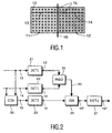
- a filter circuit of an image data set comprising a first processing stage corresponding to a first sub-step of a discrete transformation and able to process the original data and to output odd intermediate transformed data, and a first set of processing stages corresponding to a set of sub steps of the discrete transformation, able to process the odd intermediate transformed data and to deliver odd transformed data; a correction unit adapted to process the odd transformed data and to output odd corrected transform data; and a second set of processing stages corresponding to a set of sub-steps of an inverse discrete transformation, able to process the odd corrected transform data and to output intermediate filtered data, and a last processing stage corresponding to a last sub-stage. step of the inverse discrete transformation and able to process the intermediate filtered data.
- the present invention aims to provide a data filtering circuit for simply implementing the data filtering method of the prior art.
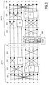
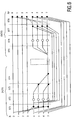
- Direct discrete cosine (DCT2) and inverse (IDCT2) transforms process the 2N concatenated data X0 to X7 using Lee's algorithm.
- the black dots represent additions or subtractions, a horizontal line in dotted lines preceding a black dot corresponding to a data item to be subtracted.
- the white dots correspond to multiplications.
- the multiplications and divisions by a power of 2 have not been represented in the diagram of FIG. 3 because they have little influence on the complexity of the implementation.
- the implementation of the correction (ZER) by zeroing the odd transformed data resulting from the global discrete transformation whose frequency is greater than the maximum predicted frequency is carried out with 4 logic circuits performing the 'AND' function between the transformed data. and outputs of a calculation circuit (PRED) of a maximum predicted frequency.
- PRED calculation circuit
- the data filtering circuit resulting from this conventional implementation would therefore lead to a complex solution comprising a DCT and an IDCT for each point of a block border.
- This solution would also have the disadvantage of being both expensive and power intensive.
- the present invention relates to a data filtering circuit for correcting block artifacts in the frequency domain. It is valid for any circuit capable of implementing in series the steps of discrete transformation of original data, correction of odd transformed data and inverse discrete transformation.
- the discrete transformation is a discrete cosine transformation.
- the present invention takes into consideration the fact that the direct and inverse calculation paths of the DCT discrete cosine transform and the Discrete Inverse IDCT cosine transform are identical and traversed in opposite directions. Thus, if the processing of a data item is not affected by the correction, the stages of Processing DCT and IDCT inverse discrete cosine transformations corresponding to this data can be suppressed to a certain extent.
- the present invention takes advantage of the fact that, for a number of data to be processed equal to a power of 2, the data paths of the odd and even transformed data are completely dissociated, as shown in FIG. 3, with the exception of a first processing stage (ST1) of the discrete cosine transformation DCT and a last processing stage (ST8) of the inverse discrete cosine transformation IDCT.
- ST1 first processing stage
- ST8 last processing stage
- the correction affecting only the odd transformed data, the processing stages located between the first and the last stage and processing the even data can be deleted.
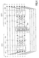
- a correction unit (ZER) of the odd transformed data is performed with 4 logic circuits performing the 'AND' function.
- the inputs of the logic circuits are on the one hand Y1, Y3, Y5 and Y7, and on the other hand an output value opposite the value provided by a PRED calculation circuit of a predicted maximum frequency. This output value is 1 if the odd transformed data YZ is of higher frequency than the maximum predicted frequency and 0 otherwise YNZ.
- the odd corrected transformed data resulting from the logical'ET 'are therefore either odd transformed data YZ to be zeroed or 0.
- the correction unit (ZER) cancels the odd transformed data YNZ other than those YZ before be set to zero.
- the odd data with h included here between 0 and 4, whose frequency is greater than the maximum predicted frequency, are not corrected while the other odd data are set to zero in order to be processed by the inverse discrete transformation. (IDCT2) so as to generate the differential data DX.
- IDCT2 inverse discrete transformation
- the last stage then acts as a differential stage, able to subtract the intermediate filtered data from the seventh floor to a first half of the data. of origin (X0-X3) and to add said intermediate filtered data to a second half of the original data (X4-X7).
- the number of operations is equal to 48, ie 36 additions and 12 multiplications, ie 32 operations less than the conventional embodiment of FIG. 3.
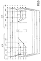
- the circuit can be simplified in some special cases. For example, when a minority of odd transformed data must be set to zero, it is possible to advantageously replace the processing path of the second half of data (X4-X7 to XF4-XF7) of FIG. 4 by a simpler processing path.
- the first stage (ST1) and the last stage remain unchanged with respect to the circuit of FIG. 4.
- the second stage (ST2) of the data filtering circuit now comprises 4 multipliers, each intermediate transformed data Odd being multiplied by a multiplicative coefficient.
- the third stage (ST3) comprises two adders respectively carrying out the sum, on the one hand data from lines 4 and 5 of the second stage, and secondly data from lines 6 and 7 of the second stage.
- the fourth stage (ST4) adds the results of these two adders, thus forming the odd transformed data YZ7.
- the fifth floor (ST5) does nothing.
- the sixth (ST6) stage duplicates the odd transformed data YZ7 for lines 4 to 7 and the seventh stage (ST7) multiplies each duplicate data by a multiplicative coefficient.
- the number of operations is only 25, that is 17 additions and 8 multiplications.
- a majority of odd transformed data must be set to zero.
- the first stage (ST1) remains unchanged with respect to the circuit of FIG. 4.
- the second stage (ST2) of the data filtering circuit according to this embodiment now comprises 4 multipliers, each odd intermediate transformed data being multiplied by a multiplicative coefficient.
- the third floor (ST3) has 2 adders respectively carrying out the sum, on the one hand data from lines 4 and 5 of the second floor, and secondly data from lines 6 and 7 of the second floor.
- the fourth stage (ST4) performs the addition of the results of these two adders, thus forming the odd transformed data YNZ1.
- the fifth stage (ST5) duplicates the opposite of the transformed data YNZ1 for lines 4 to 7.
- the sixth stage (ST6) multiplies each duplicate data by a multiplicative coefficient.
- the seventh stage (ST7) has 4 adders each performing a sum of a multiplied data and an odd intermediate transformed data of the same line.
- the eighth and last stage (ST8) has 8 adders, 4 adders performing the same subtractions as in FIG. 4 for lines 0 to 3, and 4 adders each subtracting an intermediate filtered data of line j from an original data X (j) of the same line for lines 4 to 7.
- the number of operations is equal to 29, that is 21 additions and 8 multiplications.
- Circuits such as those described in FIGS. 4, 5, 6 may be implemented in a data filtering device, a control circuit for selecting the adapted circuit from this set of circuits as a function of the number h of odd transformed data to be set to zero.
- the filtering circuit according to the invention can be integrated either as an output unit of a video decoder or as an input unit of a television receiver, in order to process decoded digital data.
- the present invention has been realized as part of the implementation of the data filtering method of the state of the art.
- the simplifications made to the filtering architecture also make it possible to improve said data filtering method.
- An instruction set contained in a programming memory may cause the circuit to perform the various steps previously described.
- the instruction set can also be loaded into the programming memory by reading a data medium such as, for example, a disk that contains the instruction set. Reading can also be done via a network of communication like, for example, the internet network. In this case, a service provider will make the instruction set available to interested parties.
Landscapes
- Engineering & Computer Science (AREA)
- Multimedia (AREA)
- Signal Processing (AREA)
- Compression Or Coding Systems Of Tv Signals (AREA)
- Image Processing (AREA)
- Picture Signal Circuits (AREA)
- Compression, Expansion, Code Conversion, And Decoders (AREA)
- Complex Calculations (AREA)
- Compression Of Band Width Or Redundancy In Fax (AREA)
Applications Claiming Priority (2)
| Application Number | Priority Date | Filing Date | Title |
|---|---|---|---|
| FR0112325 | 2001-09-25 | ||
| FR0112325 | 2001-09-25 |
Publications (3)
| Publication Number | Publication Date |
|---|---|
| EP1303142A2 EP1303142A2 (fr) | 2003-04-16 |
| EP1303142A3 EP1303142A3 (fr) | 2003-04-23 |
| EP1303142B1 true EP1303142B1 (fr) | 2006-04-26 |
Family
ID=8867585
Family Applications (1)
| Application Number | Title | Priority Date | Filing Date |
|---|---|---|---|
| EP02078817A Expired - Lifetime EP1303142B1 (fr) | 2001-09-25 | 2002-09-17 | Circuit de filtrage de données vidéo dans le domaine fréquentiel. |
Country Status (6)
| Country | Link |
|---|---|
| US (1) | US7180946B2 (enExample) |
| EP (1) | EP1303142B1 (enExample) |
| JP (1) | JP2003230143A (enExample) |
| KR (1) | KR20030026904A (enExample) |
| AT (1) | ATE324748T1 (enExample) |
| DE (1) | DE60210894T2 (enExample) |
Family Cites Families (8)
| Publication number | Priority date | Publication date | Assignee | Title |
|---|---|---|---|---|
| US5168375A (en) * | 1991-09-18 | 1992-12-01 | Polaroid Corporation | Image reconstruction by use of discrete cosine and related transforms |
| US5528528A (en) * | 1993-03-29 | 1996-06-18 | Intel Corporation | Method, apparatus, and system for transforming signals |
| US5386233A (en) * | 1993-05-13 | 1995-01-31 | Intel Corporation | Method for efficient memory use |
| US5684534A (en) * | 1993-05-26 | 1997-11-04 | Intel Corporation | Task-splitting dual-processor system for motion estimation processing |
| JPH08275160A (ja) * | 1995-03-27 | 1996-10-18 | Internatl Business Mach Corp <Ibm> | 離散余弦変換方法 |
| US6587590B1 (en) * | 1998-02-02 | 2003-07-01 | The Trustees Of The University Of Pennsylvania | Method and system for computing 8×8 DCT/IDCT and a VLSI implementation |
| US6324559B1 (en) * | 1998-10-16 | 2001-11-27 | Telefonaktiebolaget Lm Ericsson (Publ) | Odd-transform fast convolution |
| US6504872B1 (en) * | 2000-07-28 | 2003-01-07 | Zenith Electronics Corporation | Down-conversion decoder for interlaced video |
-
2002
- 2002-09-17 DE DE60210894T patent/DE60210894T2/de not_active Expired - Fee Related
- 2002-09-17 AT AT02078817T patent/ATE324748T1/de not_active IP Right Cessation
- 2002-09-17 EP EP02078817A patent/EP1303142B1/fr not_active Expired - Lifetime
- 2002-09-20 US US10/247,923 patent/US7180946B2/en not_active Expired - Fee Related
- 2002-09-25 KR KR1020020058145A patent/KR20030026904A/ko not_active Withdrawn
- 2002-09-25 JP JP2002279566A patent/JP2003230143A/ja not_active Withdrawn
Also Published As
| Publication number | Publication date |
|---|---|
| KR20030026904A (ko) | 2003-04-03 |
| ATE324748T1 (de) | 2006-05-15 |
| DE60210894D1 (de) | 2006-06-01 |
| JP2003230143A (ja) | 2003-08-15 |
| US20030076882A1 (en) | 2003-04-24 |
| US7180946B2 (en) | 2007-02-20 |
| DE60210894T2 (de) | 2006-11-30 |
| EP1303142A3 (fr) | 2003-04-23 |
| EP1303142A2 (fr) | 2003-04-16 |
Similar Documents
| Publication | Publication Date | Title |
|---|---|---|
| CN109087269B (zh) | 弱光图像增强方法及装置 | |
| EP2174289B1 (fr) | Procede de traitement d'objet numerique et systeme associe. | |
| US7916940B2 (en) | Processing of mosaic digital images | |
| Julliand et al. | Image noise and digital image forensics | |
| EP0531242A1 (fr) | Procédé de filtrage adapté d'un signal transformé en sous-bandes, et dispositif de filtrage correspondant | |
| FR2697704A1 (fr) | Procédé et dispositif de segmentation en sous-bandes et de reconstruction d'un signal numérique, et dispositif correspondant. | |
| Li et al. | Efficient burst raw denoising with variance stabilization and multi-frequency denoising network | |
| EP2656344B1 (fr) | Filtrage perfectionne dans le domaine transforme | |
| EP1303142B1 (fr) | Circuit de filtrage de données vidéo dans le domaine fréquentiel. | |
| FR2823050A1 (fr) | Dispositif implementant conjointement un post-traitement et un decodage de donnees | |
| EP1333680A2 (fr) | Procédé de traitement d'une image numérique | |
| EP1246469A2 (fr) | Procédé de réduction de format et de décodage similtanés de signaux vidéo codés | |
| EP1202577B1 (fr) | Procédé de traîtement de données vidéo | |
| FR2880453A1 (fr) | Procede et dispositif de traitement de mosaique d'images | |
| JPH0944655A (ja) | 画像処理方法および装置 | |
| EP1261209A2 (fr) | Procédé de détection de bruit dans un flux de données vidéo codées | |
| CN100473111C (zh) | 增强视频信号锐度的方法和系统 | |
| EP3072081B1 (fr) | Determination de la carte de profondeur image d'une scene | |
| EP3535730B1 (fr) | Procédé et dispositif de restauration d'image numérique | |
| EP0175623A1 (fr) | Dispositif de traitement en temps réel de signal numérique par convolution | |
| FR2832568A1 (fr) | Convertisseur numerique de frequence d'echantillonnage | |
| FR3156963A1 (fr) | Méthode de super-résolution d’image présentant une robustesse universelle | |
| KR100803045B1 (ko) | 블록기반 영상복원 장치 및 방법 | |
| FR2823338A1 (fr) | Procede et dispositif de post traitement d'images numeriques | |
| WO2007071882A2 (fr) | Procede pour fournir des donnees a un moyen de traitement numerique |
Legal Events
| Date | Code | Title | Description |
|---|---|---|---|
| PUAI | Public reference made under article 153(3) epc to a published international application that has entered the european phase |
Free format text: ORIGINAL CODE: 0009012 |
|
| PUAL | Search report despatched |
Free format text: ORIGINAL CODE: 0009013 |
|
| AK | Designated contracting states |
Designated state(s): AT BE BG CH CY CZ DE DK EE ES FI FR GB GR IE IT LI LU MC NL PT SE SK TR |
|
| AX | Request for extension of the european patent |
Extension state: AL LT LV MK RO SI |
|
| AK | Designated contracting states |
Designated state(s): AT BE BG CH CY CZ DE DK EE ES FI FR GB GR IE IT LI LU MC NL PT SE SK TR |
|
| AX | Request for extension of the european patent |
Extension state: AL LT LV MK RO SI |
|
| 17P | Request for examination filed |
Effective date: 20031023 |
|
| AKX | Designation fees paid |
Designated state(s): AT BE BG CH CY CZ DE DK EE ES FI FR GB GR IE IT LI LU MC NL PT SE SK TR |
|
| 17Q | First examination report despatched |
Effective date: 20050301 |
|
| GRAP | Despatch of communication of intention to grant a patent |
Free format text: ORIGINAL CODE: EPIDOSNIGR1 |
|
| GRAS | Grant fee paid |
Free format text: ORIGINAL CODE: EPIDOSNIGR3 |
|
| GRAA | (expected) grant |
Free format text: ORIGINAL CODE: 0009210 |
|
| AK | Designated contracting states |
Kind code of ref document: B1 Designated state(s): AT BE BG CH CY CZ DE DK EE ES FI FR GB GR IE IT LI LU MC NL PT SE SK TR |
|
| PG25 | Lapsed in a contracting state [announced via postgrant information from national office to epo] |
Ref country code: IT Free format text: LAPSE BECAUSE OF FAILURE TO SUBMIT A TRANSLATION OF THE DESCRIPTION OR TO PAY THE FEE WITHIN THE PRESCRIBED TIME-LIMIT;WARNING: LAPSES OF ITALIAN PATENTS WITH EFFECTIVE DATE BEFORE 2007 MAY HAVE OCCURRED AT ANY TIME BEFORE 2007. THE CORRECT EFFECTIVE DATE MAY BE DIFFERENT FROM THE ONE RECORDED. Effective date: 20060426 Ref country code: NL Free format text: LAPSE BECAUSE OF FAILURE TO SUBMIT A TRANSLATION OF THE DESCRIPTION OR TO PAY THE FEE WITHIN THE PRESCRIBED TIME-LIMIT Effective date: 20060426 Ref country code: AT Free format text: LAPSE BECAUSE OF FAILURE TO SUBMIT A TRANSLATION OF THE DESCRIPTION OR TO PAY THE FEE WITHIN THE PRESCRIBED TIME-LIMIT Effective date: 20060426 Ref country code: CZ Free format text: LAPSE BECAUSE OF FAILURE TO SUBMIT A TRANSLATION OF THE DESCRIPTION OR TO PAY THE FEE WITHIN THE PRESCRIBED TIME-LIMIT Effective date: 20060426 Ref country code: FI Free format text: LAPSE BECAUSE OF FAILURE TO SUBMIT A TRANSLATION OF THE DESCRIPTION OR TO PAY THE FEE WITHIN THE PRESCRIBED TIME-LIMIT Effective date: 20060426 Ref country code: IE Free format text: LAPSE BECAUSE OF FAILURE TO SUBMIT A TRANSLATION OF THE DESCRIPTION OR TO PAY THE FEE WITHIN THE PRESCRIBED TIME-LIMIT Effective date: 20060426 Ref country code: SK Free format text: LAPSE BECAUSE OF FAILURE TO SUBMIT A TRANSLATION OF THE DESCRIPTION OR TO PAY THE FEE WITHIN THE PRESCRIBED TIME-LIMIT Effective date: 20060426 |
|
| REG | Reference to a national code |
Ref country code: GB Ref legal event code: FG4D Free format text: NOT ENGLISH |
|
| REG | Reference to a national code |
Ref country code: IE Ref legal event code: FG4D Free format text: LANGUAGE OF EP DOCUMENT: FRENCH |
|
| REF | Corresponds to: |
Ref document number: 60210894 Country of ref document: DE Date of ref document: 20060601 Kind code of ref document: P |
|
| GBT | Gb: translation of ep patent filed (gb section 77(6)(a)/1977) |
Effective date: 20060605 |
|
| PG25 | Lapsed in a contracting state [announced via postgrant information from national office to epo] |
Ref country code: SE Free format text: LAPSE BECAUSE OF FAILURE TO SUBMIT A TRANSLATION OF THE DESCRIPTION OR TO PAY THE FEE WITHIN THE PRESCRIBED TIME-LIMIT Effective date: 20060726 Ref country code: DK Free format text: LAPSE BECAUSE OF FAILURE TO SUBMIT A TRANSLATION OF THE DESCRIPTION OR TO PAY THE FEE WITHIN THE PRESCRIBED TIME-LIMIT Effective date: 20060726 |
|
| PG25 | Lapsed in a contracting state [announced via postgrant information from national office to epo] |
Ref country code: ES Free format text: LAPSE BECAUSE OF FAILURE TO SUBMIT A TRANSLATION OF THE DESCRIPTION OR TO PAY THE FEE WITHIN THE PRESCRIBED TIME-LIMIT Effective date: 20060806 |
|
| PG25 | Lapsed in a contracting state [announced via postgrant information from national office to epo] |
Ref country code: PT Free format text: LAPSE BECAUSE OF FAILURE TO SUBMIT A TRANSLATION OF THE DESCRIPTION OR TO PAY THE FEE WITHIN THE PRESCRIBED TIME-LIMIT Effective date: 20060926 |
|
| PGFP | Annual fee paid to national office [announced via postgrant information from national office to epo] |
Ref country code: GB Payment date: 20060926 Year of fee payment: 5 |
|
| PG25 | Lapsed in a contracting state [announced via postgrant information from national office to epo] |
Ref country code: MC Free format text: LAPSE BECAUSE OF NON-PAYMENT OF DUE FEES Effective date: 20060930 Ref country code: CH Free format text: LAPSE BECAUSE OF NON-PAYMENT OF DUE FEES Effective date: 20060930 Ref country code: BE Free format text: LAPSE BECAUSE OF NON-PAYMENT OF DUE FEES Effective date: 20060930 Ref country code: LI Free format text: LAPSE BECAUSE OF NON-PAYMENT OF DUE FEES Effective date: 20060930 |
|
| NLV1 | Nl: lapsed or annulled due to failure to fulfill the requirements of art. 29p and 29m of the patents act | ||
| PGFP | Annual fee paid to national office [announced via postgrant information from national office to epo] |
Ref country code: DE Payment date: 20061110 Year of fee payment: 5 |
|
| REG | Reference to a national code |
Ref country code: IE Ref legal event code: FD4D |
|
| PLBE | No opposition filed within time limit |
Free format text: ORIGINAL CODE: 0009261 |
|
| STAA | Information on the status of an ep patent application or granted ep patent |
Free format text: STATUS: NO OPPOSITION FILED WITHIN TIME LIMIT |
|
| 26N | No opposition filed |
Effective date: 20070129 |
|
| REG | Reference to a national code |
Ref country code: CH Ref legal event code: PL |
|
| BERE | Be: lapsed |
Owner name: KONINKLIJKE PHILIPS ELECTRONICS N.V. Effective date: 20060930 |
|
| PG25 | Lapsed in a contracting state [announced via postgrant information from national office to epo] |
Ref country code: GR Free format text: LAPSE BECAUSE OF FAILURE TO SUBMIT A TRANSLATION OF THE DESCRIPTION OR TO PAY THE FEE WITHIN THE PRESCRIBED TIME-LIMIT Effective date: 20060727 |
|
| GBPC | Gb: european patent ceased through non-payment of renewal fee |
Effective date: 20070917 |
|
| PG25 | Lapsed in a contracting state [announced via postgrant information from national office to epo] |
Ref country code: BG Free format text: LAPSE BECAUSE OF FAILURE TO SUBMIT A TRANSLATION OF THE DESCRIPTION OR TO PAY THE FEE WITHIN THE PRESCRIBED TIME-LIMIT Effective date: 20060726 Ref country code: EE Free format text: LAPSE BECAUSE OF FAILURE TO SUBMIT A TRANSLATION OF THE DESCRIPTION OR TO PAY THE FEE WITHIN THE PRESCRIBED TIME-LIMIT Effective date: 20060426 |
|
| PG25 | Lapsed in a contracting state [announced via postgrant information from national office to epo] |
Ref country code: DE Free format text: LAPSE BECAUSE OF NON-PAYMENT OF DUE FEES Effective date: 20080401 Ref country code: TR Free format text: LAPSE BECAUSE OF FAILURE TO SUBMIT A TRANSLATION OF THE DESCRIPTION OR TO PAY THE FEE WITHIN THE PRESCRIBED TIME-LIMIT Effective date: 20060426 Ref country code: LU Free format text: LAPSE BECAUSE OF NON-PAYMENT OF DUE FEES Effective date: 20060917 |
|
| REG | Reference to a national code |
Ref country code: FR Ref legal event code: ST Effective date: 20080531 |
|
| PG25 | Lapsed in a contracting state [announced via postgrant information from national office to epo] |
Ref country code: FR Free format text: LAPSE BECAUSE OF NON-PAYMENT OF DUE FEES Effective date: 20071001 |
|
| PGFP | Annual fee paid to national office [announced via postgrant information from national office to epo] |
Ref country code: FR Payment date: 20060929 Year of fee payment: 5 |
|
| PG25 | Lapsed in a contracting state [announced via postgrant information from national office to epo] |
Ref country code: CY Free format text: LAPSE BECAUSE OF FAILURE TO SUBMIT A TRANSLATION OF THE DESCRIPTION OR TO PAY THE FEE WITHIN THE PRESCRIBED TIME-LIMIT Effective date: 20060426 Ref country code: GB Free format text: LAPSE BECAUSE OF NON-PAYMENT OF DUE FEES Effective date: 20070917 |