TECHNICAL FIELD
The present invention relates to a filter having a waveguide
tube structure for use as a high-frequency component.
TECHNICAL BACKGROUND
Typical waveguide tube filters used in microwave and
millimeter-wave bands are realized by using a resonator structure
including a metallic waveguide tube formed in a drawn structure.
This type of the filters has a drawback in larger dimensions
although it is superior in the performance thereof.
Thus, as recited in JP Patent Application 10-82184, a
pseudo waveguide tube band-pass filter is devised which has a
side wall of the waveguide tube configured by metallic via-holes
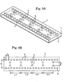
in a dielectric substrate. As a practical example, Figs. 9A and 9B
show the schematic structure of a filter having a four-stage
configuration. Fig. 9A is a perspective view thereof, whereas Fig.
9B is a top plan view thereof. A top conductor 2 is formed on one
of the surfaces of the dielectric substrate 1, whereas a bottom
conductor 3 is formed on the opposing surface thereof. Via-holes
4 connecting together the top conductor 2 and the bottom
conductor 3 are formed in two rows along the signal transfer
direction. The spacing "a" between adjacent via-holes is equal to
or below 1/2 of the in-tube wavelength. This structure is
construed as a pseudo waveguide tube having a waveguide tube
cross section defined by the thickness of the dielectric and the
spacing "b" between the two rows of the via-holes 5 arranged.
Pairs of via-holes 5 are also formed in the waveguide tube to
configure resonators having cavity lengths of L1, L2, L3 and L4.
By suitably selecting the spacing "c" between the via-holes 5
forming a pair, frequencies other than the resonant frequency can
be effectively reflected. On the other hand, a signal in the
resonant frequency passes therethrough to achieve a desired filter
function. In this filter, the dimensions of the filter are reduced
down to about 1/ ε compared to a waveguide tube having a
hollow interior (ε is the relative permittivity of the dielectric).
On the other hand, a filter is often used which is configured
by using a micro-strip line on a dielectric substrate. This filter
has relatively smaller dimensions and can be connected to a planar
circuit, such as an integrated circuit, by wire bonding, thereby
allowing the filter to be mounted in a high-frequency module with
ease.
The above waveguide tube filer is sometimes requested to
have smaller dimensions. For example, the dimensions of the
microwave or millimeter-wave integrated circuit formed on a
semiconductor device are of around 5mm square at a maximum.
Accordingly, if a small-size multi-chip module is to be
implemented by using an integrated circuit, it is generally
important to reduce the dimensions of passive components such as
a filter. In addition, it is generally difficult to connect the filter to
a planar circuit. Thus, a filter is desired which can be mounted
and connected with ease and without enlarging the dimensions
and adding a particular conversion circuit.
On the other hand, the filter using the micro-strip line
sometimes assumes a characteristic change upon mounting the
filter in a package structure. This results from the fact that the
electromagnetic field in the micro-strip line is distributed up to
the top portion thereof and thus liable to the influence by
attaching a cap member thereto.
In the connection structure using the wire bonding
technique, especially in the higher frequency range such as
millimeter wave band, there arises a characteristic change caused
by variation of the wire length or by variation of the parasitic
inductance component determined by the wire length. Such a
characteristic change is not negligible, and becomes a factor of
reducing the product yield in a mass production. For solving this
problem, a flip-chip mounting technique has been developed
wherein the millimeter-wave semiconductor integrated circuit is
mounted with face-down mounting onto a mounting board and
connected thereto by using bumps. This technique is described in
a literature, "IEEE International Solid-State Circuits Symposium,
Digest" pp.324-325, 2000, by K.Maruhashi et al., for example.
When the flip-chip mounting technique is applied, the connection
between each element and the mounting board is implemented by
a relatively short distance (200 micrometers or less), whereby the
influence by the parasitic inductance component and variation
thereof which is generally a matter of problem in the wire bonding
technique becomes negligible. For applying the flip-chip
mounting technique to the filter as well, the filter should have a
terminal adapted to a coplanar waveguide, which is generally used
for connection between elements, and should have a structure
wherein the face-down mounting scarcely changes the filter
characteristic, and thus such a filter has been strongly desired.
SUMMARY OF THE INVENTION
In view of the above, it is an object of the present invention
to provide a small-dimension filter having a dielectric waveguide
tube structure and excellent filter characteristics even in the case
of a smaller number of stages, and to provide a filter capable of
being mounted by a flip-chip mounting technique without
providing a particular external terminal thereto for connection
with a planar circuit.
The present invention provides, in a first aspect thereof, a
filter including a rectangular waveguide tube structure filled with
dielectric, wherein the rectangular waveguide structure configures
therein at least one resonator, characterized in that:
The present invention provides, in a second aspect thereof, a
filter including a rectangular waveguide tube structure including a
pair of first conductor planes formed on top and bottom surfaces
of a dielectric substrate, and a pair of second conductor planes
formed on side surfaces of the dielectric substrate, wherein the
first conductor planes constitute longer-side conductor planes, and
the rectangular waveguide tube structure configures therein at
least one resonator, characterized in that:
The present invention provides, in a third aspect thereof, a
filter including a rectangular waveguide tube structure including a
pair of conductor planes formed on top and bottom surfaces of a
dielectric substrate, conductor via-holes formed in the dielectric
substrate, wherein the conductor planes constitute longer-side
conductor planes, and the rectangular waveguide tube structure
configures at least one resonator, characterized in that:
In accordance with the filters of the present invention, it is
preferable that the slit be formed in a portion of the longer-side
conductor plane of the waveguide tube structure configuring a
central resonator among an add number of resonators arranged.
In addition, it is preferable the slit extend in a direction
perpendicular to the signal transfer direction.
It is also preferable that the conductor plane configuring the
waveguide tube structure mount thereon a coplanar waveguide,
and the coplanar waveguide be connected to the slit. In such a
case, the coplanar waveguide and a circuit board for mounting
thereon the filter are connected together via a bump.
It is also preferable that the conductor plane configuring the
waveguide tube structure mounts thereon a slot line, and the slot
line be connected to the slit. In such a case, the slot line and a
circuit board mounting thereon the filter be connected together via
a bump.
BRIEF DESCRIPTION OF THE DRAWINGS
Figs. 1A and 1B show the configuration of a filter according
to a fourth embodiment of the present invention, wherein Fig. 1A
is a perspective view and Fig. 1B is a top plan view.
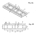
Fig. 2A and 2B show a configuration of a filter according to
a first embodiment of the present invention, wherein Fig. 2A is a
perspective view and Fig. 2B is a top plan view.
Fig. 3 is a graph showing the filter characteristic of the first
embodiment of the present invention.
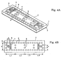
Figs. 4A and 4B show the configuration of a filter according
to a second embodiment of the present invention, wherein Fig. 4A
is a perspective view and Fig. 4B is a top plan view.
Fig. 5 is an explanatory view of the mounting structure of
the filters according to the second and fourth embodiments of the
present invention.
Fig. 6 is another explanatory view of the mounting structure
of the filters according to the second and fourth embodiments of
the present invention.
Figs. 7A and 7B show a filter according to a third
embodiment of the present invention, wherein Fig. 7A is a
perspective view and Fig. 7B is a top plan view.
Fig. 8 is an explanatory view of the mounting structure of
the filter according to the third embodiment of the present
invention.
Figs. 9A and 9B show a conventional filter, wherein Fig. 9A
is a perspective view and Fig. 9B is a top plan view.
BEST MODES FOR WORKING THE INVENTION
Hereinafter, the present invention is more specifically
described based on the preferred embodiments thereof with
reference to the drawings. Referring to Figs. 2A and 2B, there is
shown the schematic structure of a filter according to a first
embodiment of the present invention. A dielectric substrate 1 is
provided with a top conductor 2 formed on a surface thereof, and
a bottom conductor 3 formed on the opposing surface thereof.
Via-holes 4 connecting together the top conductor 2 and the
bottom conductor 3 are formed in two rows along a signal transfer
direction. The spacing "a" between adjacent via-holes is
preferably equal to or below 1/2 of the in-tube wavelength. This
structure can be construed as a pseudo waveguide tube having a
waveguide-tube cross section defined by the thickness of the
dielectric substrate (in a shorter side) and the spacing between the
two rows of the via-holes arranged (in a longer side). In the
waveguide tube, pairs of via-holes 5 are further formed, thereby
configuring resonators having cavity lengths of L1, L2 and L3.
By suitably selecting the spacing "c" between the via-holes 5
forming a pair, frequencies other than a resonant frequency can be
reflected. On the other hand, a signal in the resonant frequency
passes therethrough to achieve a desired filter property.
The present filter has a three-stage structure including three
resonators therein, wherein a portion of the top conductor 2
overlying the central resonator is provided with a slit 6 formed by
partially removing the conductor. The slit 6 is preferably
arranged to extend in a direction perpendicular to the signal
transfer direction.
Fig. 3 shows the filter characteristic (insertion loss) in the
present embodiment. The characteristics of the frequency
dependency of the insertion loss of conventional filters are also
exemplified, which include a filter having four stages similarly to
the filter shown in Fig. 4 and a filter having three stages (not
specifically shown in the drawings), both having a 3-dB pass band
similar to the 3-dB pass band of the present embodiment. For
example, the insertion loss in the present embodiment is 40dB at a
frequency (55GHz) which is 6GHz apart from the central
frequency, 61GHz, toward a lower frequency side. This value is
higher than the insertion loss, 25dB, of the conventional three-stage
filter and is approximately equal to the value, 42dB, of the
conventional four-stage filter. That is, according to the present
embodiment, an excellent suppression amount for the undesired-frequency-band
signal is obtained even in the case of using a less
number of stages compared to the conventional technique.
Accordingly, the filter has smaller dimensions, whereby lower
costs for the filter itself or smaller dimensions of a high-frequency
circuit module having such a filter can be achieved.
The operational principle of the present embodiment is that
the introduction of the slit 6 provides an attenuation pole in the
lower frequency range to thereby raise the suppression amount of
the undesired-frequency-band signal. In the present embodiment,
the attenuation pole is formed in the lower frequency range;
however, the attenuation pole may be formed in the higher
frequency range by adjusting the slit length. It is found that the
frequency at which the attenuation pole appears is easily adjusted,
without changing the other structural parameters, by changing the
slit length for the slit provided above the central resonator among
an odd number of the resonators provided in the filter. In addition,
the slit may extend between the via-holes 4, if desired, and can be
extended beyond the waveguide tube structure by increasing the
length thereof, and accordingly, a higher design choice can be
obtained. Moreover, by providing slits having different lengths
above a plurality of resonators, attenuation poles can be provided
on both the higher frequency side and the lower frequency side.
It is to be noted that although the signal electromagnetic
field leaks from the internal of the pseudo waveguide tube through
the slit, the influence by the signal electromagnetic field is lower
due to the dielectric residing within the pseudo waveguide tube.
Accordingly, if it is incorporated in a module, for example, and
covered by a cap, the influence to the filter characteristic is lower.
The filter of the present embodiment can be easily
manufactured by using a well-known alumina-ceramic-substrate
process etc. More specifically, the filter may be manufactured,
while using a ceramic-material sheet, by the steps of forming via-holes,
filling therein with metallic paste, baking, forming an
interconnection film (forming slit), plating with gold etc. It is to
be noted that the material for the substrate, the process for
forming the via-holes and the process for forming the slit are not
limited in the present invention. In addition, although the via-holes
4 are exemplarily formed in two rows along the signal
transfer direction, any number of rows may be employed so long
as the pseudo waveguide tube is configured thereby.
Referring to Figs. 4A and 4B, there is shown the schematic
structure of a filter according to a second embodiment of the
present invention. A dielectric substrate is provided with a top
conductor 2 formed on one surface thereof, and a bottom
conductor 3 formed on the opposite surface thereof. Via-holes 4
connecting the top conductor 2 and the bottom conductor 3
together are formed in two rows along the signal transfer direction.
It is preferable that the spacing "a" between adjacent via-holes be
equal to or less than 1/2 of the in-tube wavelength. This structure
can be construed as a pseudo waveguide tube having a waveguide-tube
cross section defined by the thickness of the dielectric and
the spacing "b" between the two rows of the via-holes arranged.
In addition, pairs of via-holes 5 are formed in the waveguide tube
to thereby configure resonators having cavity lengths of L1, L2,
L3 and L4. By suitably selecting the spacing "c" between the via-holes
5 forming a pair, frequencies other than the resonant
frequency can be reflected. On the other hand, a signal in the
resonant frequency passes therethrough to thereby obtain a desired
filter performance. The present filter has a four-stage structure
including four resonators therein, wherein each of portions of the
top conductor 2 overlying the outermost end resonators is
provided with slits 7 and 8 formed by partially removing the
conductor. A coplanar waveguide 9 formed on the top conductor
2 overlying the resonator is connected to the slit 7.
In accordance with the second embodiment of the present
invention, the coplanar waveguide 9 formed overlying the
resonator constitutes a terminal for external connection.
Accordingly, it can be manufactured with reduced dimensions
compared to the conventional technique (Fig. 9) which
necessitates another terminal in the signal transfer direction. In
addition, it can be connected to a planar circuit by using a
bonding wire technique without using an additional particular
conversion section. It is to be noted that although the signal
electromagnetic field leaks from the internal of the pseudo
waveguide tube through the slit, the influence thereby is lower
due to the dielectric residing within the pseudo waveguide tube.
Accordingly, if it is incorporated in a module, fore example, and
covered by a cap, the influence to the filter characteristic is lower.
Fig. 5 shows the mounting technique used for the filter
according to the present embodiment. A coplanar waveguide 13 is
formed using a conductor pattern 12 on the mounting board 11, on
which the filter 10 of the present embodiment is to be mounted.
For example, bumps 14 including gold as a main component
thereof are formed on the mounting board 11. The filter is
mounted on and connected to the mounting board 11 via bumps.
Onto this mounting board, an integrated circuit etc. may be
sometimes mounted other than the recited filter. In the present
invention, the species or fabrication method of the bums are not
particularly defined, and thus solder bumps can be used, and the
bumps may be formed on the filter side without any problem. In
this mounting technique, although the mounting board affects the
electromagnetic field leaking through the slit, the influence
thereby is relatively lower due to the dielectric residing within the
pseudo waveguide tube. For further reducing this influence, it is
possible to provide a depression in the area of the mounting board
11 in which the filter is to be mounted, for example. As described
above, in the filter according to the embodiment of the present
invention, a characteristic change between before and after the
mounting process can be suppressed, whereby advantages of the
flip-chip mounting technique can be obtained substantially
without problems of the parasitic inductance component and
variation thereof, which are generally involved in the wire
bonding process.
Referring to Figs. 7A and 7B, there is shown the schematic
structure of a filter according to a third embodiment of the present
invention. The present filter has a main structure similar to that of
the filter shown in Fig. 4, wherein a slot line 16 is connected to
the slit 7 while overstriding the slit 8. Fig. 8 shows an example of
the mounting process of the filter according to the present
embodiment. A coplanar waveguide 13 using a conductor pattern
12 is formed on the mounting board 11 on which the filter 10
according to the present embodiment is to be mounted. A slot
line/coplanar waveguide conversion section 18 is formed on the
tip of the coplanar waveguide. In addition, bumps 14 including
gold as a main component thereof are formed on the mounting
board 11. The filter is mounted on the mounting board 11 via
bumps 14 by using a heat-press technique, for example. In this
technique, the slot line formed on the filter is connected to the
coplanar waveguide on the mounting board via the slot
line/coplanar waveguide conversion section 18 with an
electromagnetic field coupling. As a result, a characteristic
change between before and after the mounting process can be
suppressed, similarly to the second embodiment, and the
advantages of the flip-chip mounting technique can be obtained
substantially without the problems of the influence by the
parasitic inductance component and the variation thereof, which
are generally involved in the wire bonding technique.
Referring to Figs. 1A and 1B, there is shown the schematic
structure of a filter according to a fourth embodiment of the
present invention. This embodiment best exhibits the features of
the present invention. A dielectric substrate 1 is provided with a
top conductor 2 formed on one surface thereof, and a bottom
conductor 3 formed on the opposite surface thereof. Via-holes 4
connecting together the top conductor 2 and the bottom conductor
3 are formed in two rows along the signal transfer direction. The
spacing "a" between adjacent via-holes is preferably equal to or
smaller than 1/2 of the in-tube wavelength. This structure is
construed as a pseudo waveguide tube having a waveguide-tube
cross section defined by the thickness of the dielectric and the
spacing "b" between two rows of the via-holes arranged. In
addition, pairs of via-holes 5 are formed in the waveguide tube to
configure resonators having cavity lengths of L1, L2 and L3. By
suitably selecting the spacing "c" between the via-holes 5 forming
a pair, frequencies other than the resonant frequency can be
reflected. On the other hand, a signal in the resonant frequency
passes therethrough to thereby obtain a desired filter property.
The present filter has a three-stage structure including three
resonators therein, wherein a portion of the top conductor 2
overlying the central resonator is provided with a slit 6 formed by
partially removing the conductor. It is preferable that the slit 6 be
"arranged to extend in the direction perpendicular to the signal
transfer direction. Each portion of the top conductor 2 overlying
the outermost end resonator is provided with slits 7 and 8 formed
by partially removing the conductor. A coplanar waveguide 9 is
connected to the slit 7. According to the present embodiment,
smaller dimensions and lower costs for the filter can be achieved,
and the flip-chip bonding technique can be applied thereto, as
recited in connection with the descriptions for the first and second
embodiments.
According to the first aspect of the present invention, by the
configurations wherein a resonator is formed in the rectangular
waveguide tube filled with dielectric, and wherein a slit is formed
in the longer-side conductor plane of the waveguide structure
configuring the resonator, an attenuation pole is configured which
improves the suppression performance for the out-of-band signal,
whereby the undesired-frequency-band signal can be suppressed
in the filter. This allows reduction of the number of stages of the
filter to reduce the dimensions thereof, whereby the filter can be
manufactured with ease and with lower costs.
The slit, as formed in the waveguide tube structure filled
with dielectric, allows reduction of the leakage of the
electromagnetic field through the slit due to the electromagnetic
field residing mainly within the dielectric, to thereby reduce the
influence to the filter characteristic.
According to the second aspect of the present invention, the
slit, as formed in the longer-side conductor plane of the
waveguide tube configuring the resonator, generates an
attenuation pole which improves the suppression performance of
the out-of-band signal, whereby the undesired-frequency-band
signal can be suppressed in the filter. This allows reduction of the
dimensions, fabrication feasibility and lower costs of the filter,
similarly to the case of the first aspect of the present invention,
whereby influence to the filter characteristic can be reduced even
in the case of the filter being mounted in a high-frequency module.
According to the third aspect of the present invention, the
slit, as formed in the longer-side conductor plane of the
waveguide tube structure configuring the resonator, generates an
attenuation pole which improves the suppression property for the
out-of-band signal, whereby the undesired-frequency-band signal
can be suppressed in the filter. This allows reduction of the
dimensions, fabrication feasibility and lower costs of the filter,
similarly to the cases of the first and second aspect of the present
invention, whereby influence to the filter characteristic can be
reduced in the case of the filter being mounted in a high-frequency
module.
In the filter of the present invention, if an odd number of
the resonators are arranged, and the slit is formed in a portion of
the longer-side conductor plane of the waveguide tube structure
overlying the central resonator among them, the attenuation pole
can be adjusted due to the symmetry without degrading the filter
characteristic, thereby providing a filter wherein the frequency at
which the attenuation pole appears can be easily adjusted.
In addition, the slit, as formed in the longer-side conductor
plane of the waveguide tube structure and extending in the
direction perpendicular to the signal transfer direction, allows an
efficient adjustment of the frequency at which the attenuation pole
appears.
The coplanar waveguide, as formed in the conductor plane
configuring the waveguide tube structure and connected to the slit,
allows connection to a planar circuit without providing a
particular external terminal or using a long-distance wire for
connecting to the terminal, whereby the filter can be reduced in
the dimensions thereof.
The structure, wherein the coplanar waveguide on the filter
and the circuit board on which the filter is mounted are connected
together via bumps, allows performing the flip-chip mounting
with ease, thereby reducing the man-hours and allowing excellent
reproducible connection in the higher-frequency range.
The structure, wherein the slot line is formed in the
conductor plane configuring the waveguide tube structure and
connected to the slit, allows connection to a planar circuit without
providing a particular external terminal and using a long-distance
wire for connecting to the terminal, thereby forming the filter in
smaller dimensions.
The structure, wherein the slot line on the filter and the
circuit board on which the filter is mounted are connected
together via bumps, allows performing the flip-chip mounting
process with ease, thereby reducing man-hours and allowing
excellent reproducible connection in the high-frequency range.