EP1300905A2 - Electronic component-mounting substrate and electronic components - Google Patents
Electronic component-mounting substrate and electronic components Download PDFInfo
- Publication number
- EP1300905A2 EP1300905A2 EP02256069A EP02256069A EP1300905A2 EP 1300905 A2 EP1300905 A2 EP 1300905A2 EP 02256069 A EP02256069 A EP 02256069A EP 02256069 A EP02256069 A EP 02256069A EP 1300905 A2 EP1300905 A2 EP 1300905A2
- Authority
- EP
- European Patent Office
- Prior art keywords
- line
- electronic component
- microstrip lines
- signal
- mounting substrate
- Prior art date
- Legal status (The legal status is an assumption and is not a legal conclusion. Google has not performed a legal analysis and makes no representation as to the accuracy of the status listed.)
- Withdrawn
Links
Images


Classifications
-
- H—ELECTRICITY
- H01—ELECTRIC ELEMENTS
- H01P—WAVEGUIDES; RESONATORS, LINES, OR OTHER DEVICES OF THE WAVEGUIDE TYPE
- H01P1/00—Auxiliary devices
- H01P1/02—Bends; Corners; Twists
-
- H—ELECTRICITY
- H01—ELECTRIC ELEMENTS
- H01P—WAVEGUIDES; RESONATORS, LINES, OR OTHER DEVICES OF THE WAVEGUIDE TYPE
- H01P5/00—Coupling devices of the waveguide type
- H01P5/02—Coupling devices of the waveguide type with invariable factor of coupling
Definitions
- the present invention relates to an electronic component-mounting substrate on which a photodiode or a laser element is mounted and an electronic component using the same.
- an optical receiver module employing a general flip-chip bonding has a structure such that a substrate 10 to which a photodiode 8 is mounted by flip-chip bonding is mounted on a package 1 provided with a lens 2 and an electrode terminal 5, as shown in Figure 1.
- a signal line 12 of the substrate 10 is bonded to the electrode terminal 5 via a ribbon wire 7, an optical fiber 3 is fixed so as to be covered with a ferrule 4, and the package 1 is sealed with a lid 6.
- a substrate to be used for such an optical receiver module is a substrate which allows flip-chip bonding of a photodiode, which has been disclosed in Japanese Unexamined Patent Publication No. Hei-10-41739, for example.
- a substrate 10 is composed of a rectangular solid-shaped dielectric 11, wherein (a) is a perspective view of the ground side, (b) is a perspective view of the signal line side, and (c) illustrates a photodiode 8 to be mounted on the substrate 10.
- symbols A-D are designated as indicating the four corners of the rectangular solid-shaped dielectric 11.
- the rectangular solid-shaped dielectric 11 for this substrate 10 is provided with microstrip lines 12 of an identical line width for a high-frequency signal (hereinafter, also referred to as a signal line) on two orthogonal surfaces thereof.
- a part of two surfaces opposed to the two signal line surfaces is a ground 13, and at this ground 13, the substrate 10 is joined to the package 1.
- a pad portion 13a is provided on one signal line surface in a manner extended from the ground 13, and bump portions 8a of the photodiode 8 are joined to these pad portions 13a.
- the drawback is that, when forming the lines, a disconnection of the signal lines 12 easily occurs at a line junction 12a on the line of the intersection between the two signal line surfaces as compared to other portions.
- an object of the present invention to provide an electronic component-mounting substrate wherein, in terms of microstrip lines formed on two surfaces which are orthogonal on a rectangular solid-shaped dielectric, joint reliability of a line junction at the line of intersection between two signal line surfaces has been enhanced.
- an object of the present invention to provide an electronic component wherein an electronic component in which high-frequency characteristics are required is mounted on a mounting substrate, and in particular an electronic component wherein deterioration of electrical characteristics can be suppressed.
- the present invention provides an electronic component-mounting substrate wherein microstrip lines for a high-frequency signal are formed on two orthogonal signal line surfaces of a rectangular-solid dielectric and a part of two surfaces opposed to these two signal line surfaces is a ground, the width of the microstrip lines being broader at junction thereof at intersecting line between these two signal line surfaces as compared with the width of the end portions of the microstrip lines.
- the cross-section of a dielectric which is perpendicular to the microstrip lines is square, and the width of the line junction of the microstrip lines at intersecting line between two signal line surfaces is designed such that if the thickness of the microstrip lines substrate be equivalently substituted with a thickness equal to the length of a diagonal line of the dielectric section, the impedance of the microstrip lines would be equivalent to an impedance at the end portion of the substituted microstrip lines.
- the present invention provides an electronic component wherein a photodiode or a laser element is mounted on the above electronic component-mounting substrate of the present invention.
- an electronic component-mounting substrate wherein joint reliability of a line junction of microstrip lines at the line of intersection between two signal line surfaces has been enhanced can be provided, and moreover, design of the lines is simple, and it becomes possible to approximate an impedance at each line portion of the microstrip lines to an objective value of an eternal signal line or the like or a fixed value, thus an increase in signal reflection and a decrease in transmission due to a line impedance mismatching can be prevented.
- an electronic component-mounting substrate of the present invention an electronic component in which an electronic component, such as a photodiode or a laser element, having preferable high-frequency characteristics is mounted without losing its characteristics can be provided.
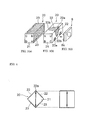
- microstrip lines (signal lines) 22 for a high-frequency signal are formed on two orthogonal signal line surfaces of a rectangular solid-shaped dielectric 21 such that the width of a line junction 22a at intersecting line between the two signal line surfaces is broader than the width of line end portions 22b.
- Figure 3(a) is a perspective view of the ground side
- Figure 3(b) is a perspective view of the signal line side
- Figure 3(c) illustrates a photodiode 8 to be mounted to the substrate 20.
- symbols A-D are designated, respectively to indicate the four corners of the rectangular solid-shaped dielectric 21.
- the joint reliability can be enhanced, and in addition, it becomes possible to approximate the impedance of the overall signal lines 22 to an impedance of an external signal line, whereby it is possible to prevent an increase in signal reflection and a decrease in transmission in a case where a high-frequency signal due to line impedance mismatching passes.
- signal line design can be carried out simply so that the impedance of each portion of the signal lines 22 becomes a desirable fixed value or approximates thereto.
- An electronic component-mounting substrate 20 as shown in Figures 3 was fabricated by using alumina with a size of 0.5 millimeters square and 5 millimeters long (specific inductive capacity of 9.5) as a rectangle solid-shaped dielectric 21. Namely, microstrip lines (signal lines) 22 were formed on two orthogonal surfaces of the dielectric 21, and a ground 23 was formed on two faces opposite to these two signal line surfaces.
- the signal lines 22 and the ground 23 were formed by depositing sequentially Ti with 0.1 ⁇ m, Ni with 0.2 ⁇ m, and Au with 2.0 ⁇ m by an evaporation method.
- the signal lines and ground may also be formed by a printing method.
- a design objective impedance of the signal lines 22 was provided as 50 ⁇ , which was the same as that of an external signal line.
- the width of both line end portions 22b was determined as 0.09mm through a calculation using, for example, a port calibration function of a simulator, the commercially available HFSS (Agilent Technologies) so that the impedance becomes 50 ⁇ .
- the width of the line junction 22a of the signal lines 22 at intersecting line between the two signal line surfaces was designed to 0.7mm by calculating using the aforementioned HFSS such that an equivalent substitution of the microstrip lines with microstrip lines substrate (right-side diagram) having a thickness equal to the length of a diagonal line of the cross-section as shown in Figure 4 would result in an impedance of 50 ⁇ .
- one line end portion 22b of the signal line 22 was provided so as to end at a mid-point of the surface, and two pad portions 23a, which were provided on both sides of this line end portion 22b so as to face each other, were joined to the ground 23 of the neighboring surface.
- a ground 23 of the neighboring surface which was continuous from the ground 23 joined to these pad portions 23a was provided by covering, as the ground 23, the whole surface from a position 0.1mm apart from the line end portion 22b adjacent at the corner A of the dielectric 21.
- the photodiode 8 was mounted by flip-chip bonding. Thereafter, as shown in Fig. 1, the substrate 20 was mounted on a package 1 which was provided with a lens 2 and an electrode terminal 5, a ribbon wire 7 was bonded, and moreover, the position of an optical fiber 3 was determined aligning so that light struck a light-receiving surface of the photodiode 8, and the optical fiber 3 was fixed with a ferrule 4. Finally, the package was shielded with a lid 6, whereby a high-frequency optical receiver module according to one example of the present invention was fabricated.
- a prior-art electronic component-mounting substrate 10 as shown in Figs. 2 (a) through (c) was fabricated.
- a dielectric 11 was of alumina with the size of 0.5 millimeters square and 5 millimeters long (specific inductive capacity of 9.5).
- signal lines 12 were formed on two orthogonal surfaces of this dielectric 11 and a ground 23 was formed on two faces opposed to these two signal line surfaces.
- a design objective impedance of the signal lines 12 was provided as 50 ⁇ , which was the same as that of an external signal line. Design was carried out so that an impedance of a section becomes 50 ⁇ with the width of both line terminal portions 12b at 0.09mm, and signal lines 12 having an identical width not only at a line junction 12a but also at other portions were used.
- one line end portion 12b of the signal line 12 was provided so as to end at a mid-point of the surface, and two pad portions 13a, which were provided on both sides of this line end portion 12b so as to face each other, were joined to the ground 13 of the neighboring surface.
- a ground 13 of the neighboring surface which was continuous from the ground 13 joined to these pad portions 13a was provided by covering, as a ground 13, the whole surface from a position 0.1mm apart from the line end portion 12b which is adjacent at the corner A of the dielectric 11.
- the photodiode 8 was mounted by flip-chip bonding. Thereafter, as shown in Fig. 1, the substrate 10 was mounted on a package 1 with a lens 2 and an electrode terminal 5. A ribbon wire 7 was bonded, and moreover, the position of an optical fiber 3 was determined by aligning so that light struck a light-receiving surface of the photodiode 8, and then the optical fiber 3 was fixed with a ferrule 4. Finally, the package was shielded with a lid 6, whereby a high-frequency optical receiver module according to one example of a prior art was fabricated.
- Reflection characteristics and transmission characteristics at signal lines of the electronic component-mounting substrate of the present invention example and prior-art example were measured. Based on the results obtained, reflection characteristics are shown in Figure 5 and transmission characteristics are shown in Figure 6. As can be understood from these results, the electronic component-mounting substrate of the present invention example at 40GHz, was improved in reflection by 4dB and in transmission by 0.7dB compared to the prior-art example.
- the present invention is not limited to the aforementioned embodiments, and various modifications can be made in terms of the material, size, application and the like, provided that it does not depart from the spirit of the present invention.
- aluminum nitride, glass ceramic or the like can be used as a dielectric, and as for an application, the electronic component-mounting substrate may be used with a high-frequency laser or the like mounted thereto.
Landscapes
- Light Receiving Elements (AREA)
- Waveguides (AREA)
- Semiconductor Lasers (AREA)
Abstract
Description
Claims (3)
- An electronic component-mounting substrate in which microstrip lines for a high-frequency signal are formed on two orthogonal signal line surfaces of a rectangular-solid dielectric, a part of two surfaces which are opposed to these two signal line surfaces is a ground, wherein the width of a line junction of the microstrip lines at intersecting line between these two signal line surfaces is broader than the width of a line end portion of the microstrip lines.
- An electronic component-mounting substrate according to Claim 1, wherein
a dielectric cross-section which is vertical to said microstrip lines is a square, and
the width of the line junction of the microstrip lines at intersecting line between two signal line surfaces is designed such that the impedance thereof would be equivalent to an impedance at a line end portion of the substituted microstrip lines, if these microstrip lines be equivalently substituted with microstrip lines on a substrate having a thickness equal to the length of a diagonal line of said section. - An electronic component wherein a photodiode or a laser element is mounted on the electronic component-mounting substrate according to Claim 1 or Claim 2.
Applications Claiming Priority (2)
| Application Number | Priority Date | Filing Date | Title |
|---|---|---|---|
| JP2001305935 | 2001-10-02 | ||
| JP2001305935A JP2003110050A (en) | 2001-10-02 | 2001-10-02 | Electronic component mounting board and electronic components |
Publications (2)
| Publication Number | Publication Date |
|---|---|
| EP1300905A2 true EP1300905A2 (en) | 2003-04-09 |
| EP1300905A3 EP1300905A3 (en) | 2003-11-26 |
Family
ID=19125649
Family Applications (1)
| Application Number | Title | Priority Date | Filing Date |
|---|---|---|---|
| EP02256069A Withdrawn EP1300905A3 (en) | 2001-10-02 | 2002-09-02 | Electronic component-mounting substrate and electronic components |
Country Status (3)
| Country | Link |
|---|---|
| EP (1) | EP1300905A3 (en) |
| JP (1) | JP2003110050A (en) |
| CA (1) | CA2398831A1 (en) |
Families Citing this family (1)
| Publication number | Priority date | Publication date | Assignee | Title |
|---|---|---|---|---|
| JP5606301B2 (en) * | 2010-12-09 | 2014-10-15 | 京セラ株式会社 | Submount substrate, optical semiconductor element storage package, and optical semiconductor device |
Family Cites Families (5)
| Publication number | Priority date | Publication date | Assignee | Title |
|---|---|---|---|---|
| US3573670A (en) * | 1969-03-21 | 1971-04-06 | Ibm | High-speed impedance-compensated circuits |
| US4647877A (en) * | 1985-03-11 | 1987-03-03 | Rockwell International Corporation | Broadband signal termination apparatus comprising series cascade of resistors and transmission lines |
| JPH0380601A (en) * | 1989-07-26 | 1991-04-05 | Mitsubishi Electric Corp | Microwave converting circuit |
| US5561405A (en) * | 1995-06-05 | 1996-10-01 | Hughes Aircraft Company | Vertical grounded coplanar waveguide H-bend interconnection apparatus |
| JPH10341027A (en) * | 1997-06-10 | 1998-12-22 | Nippon Telegr & Teleph Corp <Ntt> | Optical module |
-
2001
- 2001-10-02 JP JP2001305935A patent/JP2003110050A/en active Pending
-
2002
- 2002-08-20 CA CA002398831A patent/CA2398831A1/en not_active Abandoned
- 2002-09-02 EP EP02256069A patent/EP1300905A3/en not_active Withdrawn
Also Published As
| Publication number | Publication date |
|---|---|
| CA2398831A1 (en) | 2003-04-02 |
| EP1300905A3 (en) | 2003-11-26 |
| JP2003110050A (en) | 2003-04-11 |
Similar Documents
| Publication | Publication Date | Title |
|---|---|---|
| EP0331331B1 (en) | Subassembly for optoelectronic devices | |
| US7696628B2 (en) | Relay substrate and substrate assembly | |
| US8228686B2 (en) | Substrate for high frequency and package using this substrate | |
| US8410874B2 (en) | Vertical quasi-CPWG transmission lines | |
| EP0586760B1 (en) | Single toroid hybrid mode RF phase shifter | |
| US7306377B2 (en) | Integrated optical sub-assembly having epoxy chip package | |
| KR100575950B1 (en) | Thiocan structure photoreceiving module | |
| EP1335237A1 (en) | Electrical connection of an electro-optic element | |
| US11385422B2 (en) | Optical semiconductor device and optical module | |
| CN1116310A (en) | Electric field sensor | |
| US20210349260A1 (en) | Optical module | |
| US10085337B2 (en) | Coaxial cable assembly, electronic package and connector | |
| KR100464342B1 (en) | To-can type optical module | |
| US6796723B2 (en) | Submount for opto-electronic module and packaging method using the same | |
| CN101884118B (en) | Photoelectric conversion module | |
| US20020154362A1 (en) | Optical link module | |
| US7027674B2 (en) | Optical module and optical transmission apparatus | |
| JP4003579B2 (en) | Coplanar transmission line structure, transmission module package and transmission module | |
| US6841799B2 (en) | Optoelectronic package | |
| US6527457B2 (en) | Optical fiber guide module and a method for making the same | |
| CA2398831A1 (en) | Electronic component-mounting substrate and electronic components | |
| US20250076601A1 (en) | Optical receiving module assembly | |
| JP2009054938A (en) | Receiver module | |
| US12375179B2 (en) | Optical transceiver for high-precision bonding of flexible printed circuit board and ceramic feed-through structure and package structure | |
| JPH1056163A (en) | Integrated circuit package |
Legal Events
| Date | Code | Title | Description |
|---|---|---|---|
| PUAI | Public reference made under article 153(3) epc to a published international application that has entered the european phase |
Free format text: ORIGINAL CODE: 0009012 |
|
| AK | Designated contracting states |
Kind code of ref document: A2 Designated state(s): AT BE BG CH CY CZ DE DK EE ES FI FR GB GR IE IT LI LU MC NL PT SE SK TR Designated state(s): AT BE BG CH CY CZ DE DK EE ES FI FR GB GR IE IT LI LU MC NL PT SE SK TR |
|
| AX | Request for extension of the european patent |
Extension state: AL LT LV MK RO SI |
|
| PUAL | Search report despatched |
Free format text: ORIGINAL CODE: 0009013 |
|
| AK | Designated contracting states |
Kind code of ref document: A3 Designated state(s): AT BE BG CH CY CZ DE DK EE ES FI FR GB GR IE IT LI LU MC NL PT SE SK TR |
|
| AX | Request for extension of the european patent |
Extension state: AL LT LV MK RO SI |
|
| AKX | Designation fees paid | ||
| REG | Reference to a national code |
Ref country code: DE Ref legal event code: 8566 |
|
| STAA | Information on the status of an ep patent application or granted ep patent |
Free format text: STATUS: THE APPLICATION IS DEEMED TO BE WITHDRAWN |
|
| 18D | Application deemed to be withdrawn |
Effective date: 20040527 |