JP4003579B2 - Coplanar transmission line structure, transmission module package and transmission module - Google Patents
Coplanar transmission line structure, transmission module package and transmission module Download PDFInfo
- Publication number
- JP4003579B2 JP4003579B2 JP2002233663A JP2002233663A JP4003579B2 JP 4003579 B2 JP4003579 B2 JP 4003579B2 JP 2002233663 A JP2002233663 A JP 2002233663A JP 2002233663 A JP2002233663 A JP 2002233663A JP 4003579 B2 JP4003579 B2 JP 4003579B2
- Authority
- JP
- Japan
- Prior art keywords
- line
- signal line
- signal
- coplanar
- gnd
- Prior art date
- Legal status (The legal status is an assumption and is not a legal conclusion. Google has not performed a legal analysis and makes no representation as to the accuracy of the status listed.)
- Expired - Fee Related
Links
Images


Classifications
-
- H—ELECTRICITY
- H01—ELECTRIC ELEMENTS
- H01L—SEMICONDUCTOR DEVICES NOT COVERED BY CLASS H10
- H01L23/00—Details of semiconductor or other solid state devices
- H01L23/58—Structural electrical arrangements for semiconductor devices not otherwise provided for, e.g. in combination with batteries
- H01L23/64—Impedance arrangements
- H01L23/66—High-frequency adaptations
-
- G—PHYSICS
- G02—OPTICS
- G02B—OPTICAL ELEMENTS, SYSTEMS OR APPARATUS
- G02B6/00—Light guides; Structural details of arrangements comprising light guides and other optical elements, e.g. couplings
- G02B6/24—Coupling light guides
- G02B6/42—Coupling light guides with opto-electronic elements
- G02B6/4201—Packages, e.g. shape, construction, internal or external details
- G02B6/4274—Electrical aspects
- G02B6/4279—Radio frequency signal propagation aspects of the electrical connection, high frequency adaptations
-
- H—ELECTRICITY
- H01—ELECTRIC ELEMENTS
- H01L—SEMICONDUCTOR DEVICES NOT COVERED BY CLASS H10
- H01L23/00—Details of semiconductor or other solid state devices
- H01L23/02—Containers; Seals
- H01L23/04—Containers; Seals characterised by the shape of the container or parts, e.g. caps, walls
- H01L23/053—Containers; Seals characterised by the shape of the container or parts, e.g. caps, walls the container being a hollow construction and having an insulating or insulated base as a mounting for the semiconductor body
- H01L23/057—Containers; Seals characterised by the shape of the container or parts, e.g. caps, walls the container being a hollow construction and having an insulating or insulated base as a mounting for the semiconductor body the leads being parallel to the base
-
- H—ELECTRICITY
- H01—ELECTRIC ELEMENTS
- H01L—SEMICONDUCTOR DEVICES NOT COVERED BY CLASS H10
- H01L2223/00—Details relating to semiconductor or other solid state devices covered by the group H01L23/00
- H01L2223/58—Structural electrical arrangements for semiconductor devices not otherwise provided for
- H01L2223/64—Impedance arrangements
- H01L2223/66—High-frequency adaptations
- H01L2223/6605—High-frequency electrical connections
- H01L2223/6611—Wire connections
-
- H—ELECTRICITY
- H01—ELECTRIC ELEMENTS
- H01L—SEMICONDUCTOR DEVICES NOT COVERED BY CLASS H10
- H01L2223/00—Details relating to semiconductor or other solid state devices covered by the group H01L23/00
- H01L2223/58—Structural electrical arrangements for semiconductor devices not otherwise provided for
- H01L2223/64—Impedance arrangements
- H01L2223/66—High-frequency adaptations
- H01L2223/6605—High-frequency electrical connections
- H01L2223/6627—Waveguides, e.g. microstrip line, strip line, coplanar line
-
- H—ELECTRICITY
- H01—ELECTRIC ELEMENTS
- H01L—SEMICONDUCTOR DEVICES NOT COVERED BY CLASS H10
- H01L2224/00—Indexing scheme for arrangements for connecting or disconnecting semiconductor or solid-state bodies and methods related thereto as covered by H01L24/00
- H01L2224/01—Means for bonding being attached to, or being formed on, the surface to be connected, e.g. chip-to-package, die-attach, "first-level" interconnects; Manufacturing methods related thereto
- H01L2224/02—Bonding areas; Manufacturing methods related thereto
- H01L2224/04—Structure, shape, material or disposition of the bonding areas prior to the connecting process
- H01L2224/05—Structure, shape, material or disposition of the bonding areas prior to the connecting process of an individual bonding area
- H01L2224/0554—External layer
- H01L2224/05599—Material
-
- H—ELECTRICITY
- H01—ELECTRIC ELEMENTS
- H01L—SEMICONDUCTOR DEVICES NOT COVERED BY CLASS H10
- H01L2224/00—Indexing scheme for arrangements for connecting or disconnecting semiconductor or solid-state bodies and methods related thereto as covered by H01L24/00
- H01L2224/01—Means for bonding being attached to, or being formed on, the surface to be connected, e.g. chip-to-package, die-attach, "first-level" interconnects; Manufacturing methods related thereto
- H01L2224/42—Wire connectors; Manufacturing methods related thereto
- H01L2224/44—Structure, shape, material or disposition of the wire connectors prior to the connecting process
- H01L2224/45—Structure, shape, material or disposition of the wire connectors prior to the connecting process of an individual wire connector
- H01L2224/45001—Core members of the connector
- H01L2224/45099—Material
- H01L2224/451—Material with a principal constituent of the material being a metal or a metalloid, e.g. boron (B), silicon (Si), germanium (Ge), arsenic (As), antimony (Sb), tellurium (Te) and polonium (Po), and alloys thereof
- H01L2224/45138—Material with a principal constituent of the material being a metal or a metalloid, e.g. boron (B), silicon (Si), germanium (Ge), arsenic (As), antimony (Sb), tellurium (Te) and polonium (Po), and alloys thereof the principal constituent melting at a temperature of greater than or equal to 950°C and less than 1550°C
- H01L2224/45144—Gold (Au) as principal constituent
-
- H—ELECTRICITY
- H01—ELECTRIC ELEMENTS
- H01L—SEMICONDUCTOR DEVICES NOT COVERED BY CLASS H10
- H01L2224/00—Indexing scheme for arrangements for connecting or disconnecting semiconductor or solid-state bodies and methods related thereto as covered by H01L24/00
- H01L2224/01—Means for bonding being attached to, or being formed on, the surface to be connected, e.g. chip-to-package, die-attach, "first-level" interconnects; Manufacturing methods related thereto
- H01L2224/42—Wire connectors; Manufacturing methods related thereto
- H01L2224/47—Structure, shape, material or disposition of the wire connectors after the connecting process
- H01L2224/48—Structure, shape, material or disposition of the wire connectors after the connecting process of an individual wire connector
- H01L2224/481—Disposition
- H01L2224/48151—Connecting between a semiconductor or solid-state body and an item not being a semiconductor or solid-state body, e.g. chip-to-substrate, chip-to-passive
- H01L2224/48221—Connecting between a semiconductor or solid-state body and an item not being a semiconductor or solid-state body, e.g. chip-to-substrate, chip-to-passive the body and the item being stacked
- H01L2224/48225—Connecting between a semiconductor or solid-state body and an item not being a semiconductor or solid-state body, e.g. chip-to-substrate, chip-to-passive the body and the item being stacked the item being non-metallic, e.g. insulating substrate with or without metallisation
- H01L2224/48227—Connecting between a semiconductor or solid-state body and an item not being a semiconductor or solid-state body, e.g. chip-to-substrate, chip-to-passive the body and the item being stacked the item being non-metallic, e.g. insulating substrate with or without metallisation connecting the wire to a bond pad of the item
-
- H—ELECTRICITY
- H01—ELECTRIC ELEMENTS
- H01L—SEMICONDUCTOR DEVICES NOT COVERED BY CLASS H10
- H01L2224/00—Indexing scheme for arrangements for connecting or disconnecting semiconductor or solid-state bodies and methods related thereto as covered by H01L24/00
- H01L2224/01—Means for bonding being attached to, or being formed on, the surface to be connected, e.g. chip-to-package, die-attach, "first-level" interconnects; Manufacturing methods related thereto
- H01L2224/42—Wire connectors; Manufacturing methods related thereto
- H01L2224/47—Structure, shape, material or disposition of the wire connectors after the connecting process
- H01L2224/49—Structure, shape, material or disposition of the wire connectors after the connecting process of a plurality of wire connectors
- H01L2224/491—Disposition
- H01L2224/4911—Disposition the connectors being bonded to at least one common bonding area, e.g. daisy chain
-
- H—ELECTRICITY
- H01—ELECTRIC ELEMENTS
- H01L—SEMICONDUCTOR DEVICES NOT COVERED BY CLASS H10
- H01L2224/00—Indexing scheme for arrangements for connecting or disconnecting semiconductor or solid-state bodies and methods related thereto as covered by H01L24/00
- H01L2224/01—Means for bonding being attached to, or being formed on, the surface to be connected, e.g. chip-to-package, die-attach, "first-level" interconnects; Manufacturing methods related thereto
- H01L2224/42—Wire connectors; Manufacturing methods related thereto
- H01L2224/47—Structure, shape, material or disposition of the wire connectors after the connecting process
- H01L2224/49—Structure, shape, material or disposition of the wire connectors after the connecting process of a plurality of wire connectors
- H01L2224/491—Disposition
- H01L2224/4912—Layout
- H01L2224/49171—Fan-out arrangements
-
- H—ELECTRICITY
- H01—ELECTRIC ELEMENTS
- H01L—SEMICONDUCTOR DEVICES NOT COVERED BY CLASS H10
- H01L2224/00—Indexing scheme for arrangements for connecting or disconnecting semiconductor or solid-state bodies and methods related thereto as covered by H01L24/00
- H01L2224/80—Methods for connecting semiconductor or other solid state bodies using means for bonding being attached to, or being formed on, the surface to be connected
- H01L2224/85—Methods for connecting semiconductor or other solid state bodies using means for bonding being attached to, or being formed on, the surface to be connected using a wire connector
- H01L2224/8538—Bonding interfaces outside the semiconductor or solid-state body
- H01L2224/85399—Material
-
- H—ELECTRICITY
- H01—ELECTRIC ELEMENTS
- H01L—SEMICONDUCTOR DEVICES NOT COVERED BY CLASS H10
- H01L24/00—Arrangements for connecting or disconnecting semiconductor or solid-state bodies; Methods or apparatus related thereto
- H01L24/01—Means for bonding being attached to, or being formed on, the surface to be connected, e.g. chip-to-package, die-attach, "first-level" interconnects; Manufacturing methods related thereto
- H01L24/42—Wire connectors; Manufacturing methods related thereto
- H01L24/44—Structure, shape, material or disposition of the wire connectors prior to the connecting process
- H01L24/45—Structure, shape, material or disposition of the wire connectors prior to the connecting process of an individual wire connector
-
- H—ELECTRICITY
- H01—ELECTRIC ELEMENTS
- H01L—SEMICONDUCTOR DEVICES NOT COVERED BY CLASS H10
- H01L24/00—Arrangements for connecting or disconnecting semiconductor or solid-state bodies; Methods or apparatus related thereto
- H01L24/01—Means for bonding being attached to, or being formed on, the surface to be connected, e.g. chip-to-package, die-attach, "first-level" interconnects; Manufacturing methods related thereto
- H01L24/42—Wire connectors; Manufacturing methods related thereto
- H01L24/47—Structure, shape, material or disposition of the wire connectors after the connecting process
- H01L24/48—Structure, shape, material or disposition of the wire connectors after the connecting process of an individual wire connector
-
- H—ELECTRICITY
- H01—ELECTRIC ELEMENTS
- H01L—SEMICONDUCTOR DEVICES NOT COVERED BY CLASS H10
- H01L24/00—Arrangements for connecting or disconnecting semiconductor or solid-state bodies; Methods or apparatus related thereto
- H01L24/01—Means for bonding being attached to, or being formed on, the surface to be connected, e.g. chip-to-package, die-attach, "first-level" interconnects; Manufacturing methods related thereto
- H01L24/42—Wire connectors; Manufacturing methods related thereto
- H01L24/47—Structure, shape, material or disposition of the wire connectors after the connecting process
- H01L24/49—Structure, shape, material or disposition of the wire connectors after the connecting process of a plurality of wire connectors
-
- H—ELECTRICITY
- H01—ELECTRIC ELEMENTS
- H01L—SEMICONDUCTOR DEVICES NOT COVERED BY CLASS H10
- H01L2924/00—Indexing scheme for arrangements or methods for connecting or disconnecting semiconductor or solid-state bodies as covered by H01L24/00
- H01L2924/0001—Technical content checked by a classifier
- H01L2924/00014—Technical content checked by a classifier the subject-matter covered by the group, the symbol of which is combined with the symbol of this group, being disclosed without further technical details
-
- H—ELECTRICITY
- H01—ELECTRIC ELEMENTS
- H01L—SEMICONDUCTOR DEVICES NOT COVERED BY CLASS H10
- H01L2924/00—Indexing scheme for arrangements or methods for connecting or disconnecting semiconductor or solid-state bodies as covered by H01L24/00
- H01L2924/01—Chemical elements
- H01L2924/01079—Gold [Au]
-
- H—ELECTRICITY
- H01—ELECTRIC ELEMENTS
- H01L—SEMICONDUCTOR DEVICES NOT COVERED BY CLASS H10
- H01L2924/00—Indexing scheme for arrangements or methods for connecting or disconnecting semiconductor or solid-state bodies as covered by H01L24/00
- H01L2924/10—Details of semiconductor or other solid state devices to be connected
- H01L2924/11—Device type
- H01L2924/12—Passive devices, e.g. 2 terminal devices
- H01L2924/1204—Optical Diode
- H01L2924/12042—LASER
-
- H—ELECTRICITY
- H01—ELECTRIC ELEMENTS
- H01L—SEMICONDUCTOR DEVICES NOT COVERED BY CLASS H10
- H01L2924/00—Indexing scheme for arrangements or methods for connecting or disconnecting semiconductor or solid-state bodies as covered by H01L24/00
- H01L2924/10—Details of semiconductor or other solid state devices to be connected
- H01L2924/11—Device type
- H01L2924/12—Passive devices, e.g. 2 terminal devices
- H01L2924/1204—Optical Diode
- H01L2924/12043—Photo diode
-
- H—ELECTRICITY
- H01—ELECTRIC ELEMENTS
- H01L—SEMICONDUCTOR DEVICES NOT COVERED BY CLASS H10
- H01L2924/00—Indexing scheme for arrangements or methods for connecting or disconnecting semiconductor or solid-state bodies as covered by H01L24/00
- H01L2924/15—Details of package parts other than the semiconductor or other solid state devices to be connected
- H01L2924/151—Die mounting substrate
- H01L2924/1517—Multilayer substrate
- H01L2924/15172—Fan-out arrangement of the internal vias
- H01L2924/15173—Fan-out arrangement of the internal vias in a single layer of the multilayer substrate
-
- H—ELECTRICITY
- H01—ELECTRIC ELEMENTS
- H01L—SEMICONDUCTOR DEVICES NOT COVERED BY CLASS H10
- H01L2924/00—Indexing scheme for arrangements or methods for connecting or disconnecting semiconductor or solid-state bodies as covered by H01L24/00
- H01L2924/19—Details of hybrid assemblies other than the semiconductor or other solid state devices to be connected
- H01L2924/1901—Structure
- H01L2924/1903—Structure including wave guides
-
- H—ELECTRICITY
- H01—ELECTRIC ELEMENTS
- H01L—SEMICONDUCTOR DEVICES NOT COVERED BY CLASS H10
- H01L2924/00—Indexing scheme for arrangements or methods for connecting or disconnecting semiconductor or solid-state bodies as covered by H01L24/00
- H01L2924/19—Details of hybrid assemblies other than the semiconductor or other solid state devices to be connected
- H01L2924/191—Disposition
- H01L2924/19101—Disposition of discrete passive components
- H01L2924/19107—Disposition of discrete passive components off-chip wires
-
- H—ELECTRICITY
- H01—ELECTRIC ELEMENTS
- H01L—SEMICONDUCTOR DEVICES NOT COVERED BY CLASS H10
- H01L2924/00—Indexing scheme for arrangements or methods for connecting or disconnecting semiconductor or solid-state bodies as covered by H01L24/00
- H01L2924/30—Technical effects
- H01L2924/301—Electrical effects
- H01L2924/3011—Impedance
Landscapes
- Physics & Mathematics (AREA)
- General Physics & Mathematics (AREA)
- Condensed Matter Physics & Semiconductors (AREA)
- Engineering & Computer Science (AREA)
- Computer Hardware Design (AREA)
- Microelectronics & Electronic Packaging (AREA)
- Power Engineering (AREA)
- Optics & Photonics (AREA)
- Waveguides (AREA)
- Semiconductor Lasers (AREA)
Description
【0001】
【発明の属する技術分野】
本発明は、光伝送装置等で用いられるコプレーナ線路構造、伝送モジュール用パッケージ及び伝送モジュールに関するものである。
【0002】
【従来の技術】
例えば半導体パッケージには、当該パッケージに実装されるアンプ等の半導体素子と外部基板等とを電気的に接続するためのコプレーナ線路構造を有するものがある。コプレーナ線路は、信号ラインと、信号ラインの両側に配置されたGND(接地)プレーンとを有する線路である。ところで、半導体素子の端子ピッチは数百μm以下と狭いため、パッケージの内側部分では、それに合わせて信号ラインとGNDプレーンとの間隔及び信号ラインの幅が狭くなっている。一方、パッケージの外側部分では、外部基板等との接続を考慮して、信号ラインとGNDプレーンとの間隔が数mm程度、信号ラインの幅が数mm程度と広くなっている。このため、コプレーナ線路構造には、信号ラインとGNDプレーンとの間隔及び信号ラインの幅を徐々に変化させた部分が形成されている。
【0003】
【発明が解決しようとする課題】
一般的なコプレーナ線路では、狭ピッチであるパッケージ内側の信号ラインと広ピッチであるパッケージ外側の信号ラインとを単に直線的につないだ構造となっているが、この場合には信号ラインの伝送特性が劣化するという不具合があった。
【0004】
本発明の目的は、伝送特性を向上させることができるコプレーナ線路構造、伝送モジュール用パッケージ及び伝送モジュールを提供することである。
【0005】
【課題を解決するための手段】
本発明者らは、鋭意検討を重ねた結果、コプレーナ線路の特性インピーダンスは、信号ラインと接地プレーンとの間隔(信号/GND間隔)及び信号ライン幅で決定されるが、特性インピーダンスが一定となるような信号ライン幅と信号/GND間隔との関係は、1次関数的な変化でなく指数関数的な変化を示すことを見い出した。そして、更に検討を重ねたところ、信号/GND間隔が狭ピッチな部分の信号ライン及びGNDプレーンと信号/GND間隔が広ピッチな部分の信号ライン及びGNDプレーンとを直線的につないだ構造では、その部分がインピーダンス不整合を起こし、その結果として伝送特性の劣化を引き起こしていると考え、本発明を完成させるに至った。
【0006】
即ち、本発明は、信号ラインと、信号ラインの両側に配置された接地プレーンとを有するコプレーナ線路構造において、信号ラインと接地プレーンとの間隔及び信号ラインの幅が、一端側から他端側に向けて広がるように形成された線路寸法変化部を有し、線路寸法変化部での特性インピーダンスが所定値になるように、線路寸法変化部における信号ラインと接地プレーンとの間隔が信号ラインの幅の変化に対して指数関数的に変化していることを特徴とするものである。
【0007】
このように線路寸法変化部における信号ラインと接地プレーンとの間隔を、一端側から他端側に向けて信号ラインの幅の広がりに対して指数関数的に広げることにより、コプレーナ線路の特性インピーダンスが線路寸法変化部においてほぼ一定になる。従って、インピーダンス不整合に起因した信号ラインの伝送特性の劣化を低減することができる。
【0008】
好ましくは、線路寸法変化部は、信号ラインの両エッジ及び接地プレーンの信号ライン側のエッジが一端側から他端側に向けて曲線的に延在するように形成されている。この場合には、線路寸法変化部の両端部、つまり信号ラインと接地プレーンとの間隔及び信号ラインの幅が変化し始める部位において、信号ラインの両エッジ及び接地プレーンの信号ライン側のエッジがいずれも滑らかに変化するようになる。このため、線路寸法変化部の両端部においてコプレーナ線路の特性インピーダンスが一時的に急激に変化することが確実に防止されるので、信号ラインの伝送特性が更に向上する。
【0009】
本発明の伝送モジュール用パッケージは、上記のコプレーナ線路構造を有することを特徴とするものである。この場合には、上述したように、コプレーナ線路の特性インピーダンスがほぼ一定になるため、信号ラインの伝送特性が向上する。
【0010】
本発明の伝送モジュールは、上記のパッケージと、信号ライン及び接地プレーンと電気的に接続された電気部品とを備えたことを特徴とするものである。この場合には、上述したように、コプレーナ線路の特性インピーダンスがほぼ一定になるため、信号ラインの伝送特性が向上する。
【0011】
【発明の実施の形態】
以下、本発明に係るコプレーナ線路構造、伝送モジュール用パッケージ及び伝送モジュールの好適な実施形態について図面を参照して説明する。
【0012】
図1は、本発明に係るコプレーナ線路構造の一実施形態を示す構成図である。同図において、本実施形態のコプレーナ線路基板1は、半導体素子2と外部基板3とを電気的に接続するための線路基板である。
【0013】
半導体素子2は、信号端子4と、この信号端子4の両側に配置されたGND(接地)端子5とを有している。外部基板3は、信号ライン6と、この信号ライン6の両側に配置されたGND(接地)プレーン7とを有している。外部基板3における信号ライン6とGNDプレーン7との間隔Dwは、半導体素子2における信号端子4とGND端子5との間隔Dnよりも大きくなっている。また、外部基板3における信号ライン6の幅Swは、半導体素子2における信号端子4の幅Snよりも大きくなっている。
【0014】
コプレーナ線路基板1は、例えばAl2O3等で形成された基板本体8を有している。この基板本体8の表面には、信号ライン9と、この信号ライン9の両側に位置するGNDプレーン10とが設けられている。信号ライン9及びGNDプレーン10は、Au等の金属のパターンで形成されている。
【0015】
また、コプレーナ線路基板1は、半導体素子2側に配置された線路狭ピッチ部11と、外部基板3側に配置された線路広ピッチ部12と、線路狭ピッチ部11と線路広ピッチ部12との間に配置された線路寸法変化部13とからなっている。
【0016】
線路狭ピッチ部11においては、信号ライン9とGNDプレーン10との間隔D1が0.05mmと一定であり、信号ライン9の幅S1が0.1mmと一定である。線路広ピッチ部12においては、信号ライン9とGNDプレーン10との間隔D2が0.35mmと一定であり、信号ライン9の幅S2が0.5mmと一定である。なお、これらの寸法は、コプレーナ線路基板1の特性インピーダンスZ0が50Ωになるように構成したものである。線路寸法変化部13においては、信号ライン9とGNDプレーン10との間隔(信号/GND間隔)D3及び信号ライン9の幅(信号ライン幅)S3が、線路狭ピッチ部11から線路広ピッチ部12に向けて徐々に広くなっている。
【0017】
線路狭ピッチ部11における信号ライン9及びGNDプレーン10は、半導体素子2における信号端子4及びGND端子5と金ワイヤ14でそれぞれ電気的に接続されている。線路広ピッチ部12における信号ライン9及びGNDプレーン10は、外部基板3における信号ライン6及びGNDプレーン7と金ワイヤ15でそれぞれ電気的に接続されている。
【0018】
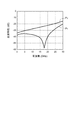
このようなコプレーナ線路基板1において、線路寸法変化部13における特性インピーダンスZ0が50Ωになるようにコプレーナ線路の条件を計算(シミュレーション)した結果を図2に示す。同図から分かるように、特性インピーダンスZ0が50Ωとなるような信号ライン幅xと信号/GND間隔yとの関係は、下記式のような指数関数で表される。
【0019】
y=0.030383*e^(4.9158x) …(A)
コプレーナ線路基板1の線路寸法変化部13では、信号/GND間隔D3が信号ライン幅S3の変化に対して上記(A)式の関係をもって指数関数的に変化するように形成されている。これにより、線路寸法変化部13での特性インピーダンスZ0がほぼ50Ωで一定となる。
【0020】
このとき、線路寸法変化部13における信号ライン9の両エッジ9a及び接地プレーン10の信号ライン9側のエッジ10aのいずれもが、線路狭ピッチ部11から線路広ピッチ部12まで曲線的に延在しているのが好ましい。これにより、線路寸法変化部13と線路狭ピッチ部11及び線路広ピッチ部12との境界部において、信号/GND間隔D3及び信号ライン幅S3が滑らかに変化した状態で、信号ライン幅S3の変化に対して信号/GND間隔D3が指数関数的に変化するようになる。従って、線路寸法変化部13と線路狭ピッチ部11及び線路広ピッチ部12との境界部での特性インピーダンスZ0もほぼ50Ωになる。
【0021】
以上により、コプレーナ線路基板1の特性インピーダンスZ0は全体的に一定になるので、インピーダンス不整合による信号ラインの伝送特性の劣化が低減される。その結果、コプレーナ線路基板の伝送特性を向上させることができる。
【0022】
次に、図3(a)に示すような本実施形態のコプレーナ線路構造と、図3(b)に示すような従来一般のコプレーナ線路構造とで、伝送特性の比較を行った実施例について説明する。
【0023】
図3(b)に示すコプレーナ線路構造においては、線路寸法変化部における信号ライン16の両エッジ16a及び接地プレーン17のエッジ17aが直線的に延びている。この場合、線路寸法変化部では、信号ライン幅S3の変化に対して信号/GND間隔D3が、図2の点線で示すように一次関数的に変化するようになるため、特性インピーダンスZ0の不整合が生じる。
【0024】
図4は、コプレーナ線路の伝送特性として反射特性のシミュレーション結果を示したものである。この反射特性は、例えば信号ラインの線路狭ピッチ部側ポートから導入した信号(入射波)のパワーと線路狭ピッチ部側ポートに反射して戻る信号(反射波)のパワーとの比を表わしたものである。
【0025】
このとき、コプレーナ線路基板の厚さは0.6mmであり、比誘電率は8.5であり、材質はAl2O3である。また、図4において、特性P1が図3(a)に示すコプレーナ線路構造の反射特性を示し、特性P2が図3(b)に示すコプレーナ線路構造の反射特性を示している。
【0026】
同図より、図3(a)に示す本実施形態のコプレーナ線路構造では、図3(b)に示すコプレーナ線路構造に比べて反射特性が改善されていることが分かる。特に周波数18GHz付近を中心とした帯域では、反射特性が大きく改善されている。このような特性は、コプレーナ線路基板の線路寸法変化部の長さやコプレーナ線路基板の材質、比誘電率の違いによって異なると考えられる。そこで、線路寸法変化部の長さやコプレーナ線路基板の材質、比誘電率を適宜変えることによって、任意の周波数帯域における反射特性を大幅に向上させることが可能となる。
【0027】
図5は、コプレーナ線路の伝送特性として挿入損失特性のシミュレーション結果を示したものである。この挿入損失特性は、例えば信号ラインの線路狭ピッチ部側ポートから導入した信号(入射波)のパワーと線路広ピッチ部側ポートから出力される信号(透過波)のパワーとの比を表わしたものである。
【0028】
この時のコプレーナ線路基板の厚さ、比誘電率、材質は上記と同様である。また、図5において、特性Q1が図3(a)に示すコプレーナ線路構造の挿入損失特性を示し、特性Q2が図3(b)に示すコプレーナ線路構造の挿入損失特性を示している。
【0029】
同図より、図3(a)に示す本実施形態のコプレーナ線路構造では、図3(b)に示すコプレーナ線路構造に比べて挿入損失特性が改善されていることが分かる。このとき、周波数が高くなるほど、挿入損失特性が良くなっている。従って、本実施形態のコプレーナ線路構造を高周波信号ラインに適用した場合に、特に効果的である。
【0030】
図6は、本発明に係る伝送モジュールの一実施形態として、上述したコプレーナ線路構造を有する受光モジュールを示す構成図である。同図において、受光モジュール20は、矩形状の半導体パッケージ21を有し、この半導体パッケージ21には部品実装基板22が設けられている。この部品実装基板22には、ファイバ固定部材23、受光素子(フォトダイオード)24、アンプ25が並列に実装されている。なお、当該部品実装基板22は半導体パッケージ21の底部板でもあるが、部品実装基板として別途専用の基板を設けてもよい。
【0031】
ファイバ固定部材23は、光ファイバ心線26の裸ファイバ26aを位置決めして固定する。受光素子24は、光ファイバ心線26からの光信号を受光して電気信号に変換する。アンプ25は、受光素子24からの電気信号を増幅して出力する。
【0032】
また、半導体パッケージ21における部品実装基板22の一側には、コプレーナ線路基板27が設けられている。コプレーナ線路基板27は、GNDプレーン28と、このGNDプレーン28の両側に配置された信号ライン29と、各信号ライン29の外側に配置されたGNDプレーン30とを有している。コプレーナ線路基板27は、信号ライン29とGNDプレーン28,30との間隔が信号ライン29の幅の変化に対して指数関数的に変化するように形成された部分を有している。これにより、コプレーナ線路基板27は、GNDプレーン28を共通として上述したコプレーナ線路構造を2組有することとなる。
【0033】
また、半導体パッケージ21には、GNDプレーン31、電源ライン32、モニタライン33が設けられている。GNDプレーン30,31、電源ライン32、モニタライン33にはリードピン34が接合されている。
【0034】
アンプ25は、図示はしないが、GNDプレーン28,30、信号ライン29、電源ライン32、モニタライン33と金ワイヤでそれぞれ接続されている。これにより、リードピン34及び電源ライン32によってアンプ25に所定の電力が供給される。そして、アンプ25の出力信号が、信号ライン29を介して外部基板(図示せず)に送られる。また、モニタ信号が、モニタライン33及びリードピン34を介して外部基板(図示せず)に送られる。
【0035】
図7は、本発明に係る伝送モジュールの他の実施形態として、上述したコプレーナ線路構造を有する増幅モジュールを示す構成図である。同図において、増幅モジュール40は、矩形状の半導体パッケージ41を有し、この半導体パッケージ41には部品実装基板42が設けられ、この部品実装基板42にはアンプ43が実装されている。なお、ここでは部品実装基板42を設けたが、アンプ43を半導体パッケージ41に直接実装してもよい。
【0036】
半導体パッケージ41における部品実装基板42の両側には、コプレーナ線路基板44がそれぞれ設けられている。コプレーナ線路基板44は、信号ライン45と、この信号ライン45の両側に配置されたGNDプレーン46とを有している。コプレーナ線路基板44は、信号ライン45とGNDプレーン46との間隔が信号ライン45の幅の変化に対して指数関数的に変化するように形成された部分を有している。また、半導体パッケージ41には、電源ライン47とモニタライン48とが設けられている。
【0037】
アンプ43は、信号ライン45、GNDプレーン46、電源ライン47及びモニタライン48と金ワイヤ49で接続されている。これにより、電源ライン47によってアンプ43に所定の電力が供給される。そして、外部基板(図示せず)から一方の信号ライン45を介して送られてきた電気信号がアンプ43で増幅され、その信号が他方の信号ライン45を介して他の外部基板(図示せず)に送られる。また、モニタ信号が、モニタライン48を介して外部基板(図示せず)に送られる。
【0038】
なお、本発明は、上記実施形態に限定されるものではない。例えば、上記実施形態のコプレーナ線路構造では、線路寸法変化部13における信号ライン9のエッジ9a及び接地プレーン10のエッジ10aが共に曲線的に延びるようにしたが、特にこれには限られない。つまり、信号ライン幅S3の変化に対して信号/GND間隔D3が指数関数的に変化するのであれば、信号ライン9のエッジ9a及び接地プレーン10のエッジ10aのいずれか一方が直線的に延びるようにしても良い。
【0039】
また、上記実施形態のコプレーナ線路構造では、コプレーナ線路基板1の特性インピーダンスZ0が50Ωで一定となるように構成したが、特にこれに限らず、例えば特性インピーダンスZ0が75Ωで一定となるように、信号ライン幅S3の変化に対して信号/GND間隔D3を指数関数的に変化させても良い。
【0040】
さらに、上記実施形態では、伝送モジュールの例として受光モジュール及び増幅モジュールを挙げたが、本発明は、発光モジュールなど他の伝送モジュールにも適用可能である。
【0041】
【発明の効果】
本発明によれば、線路寸法変化部における信号ラインと接地プレーンとの間隔を信号ラインの幅の変化に対して指数関数的に変化させる構成としたので、信号ラインの伝送特性を向上させることができる。
【図面の簡単な説明】
【図1】本発明に係るコプレーナ線路構造の一実施形態を示す構成図である。
【図2】図1に示す線路寸法変化部における特性インピーダンスが50Ωになるような信号ライン幅と信号/GND間隔との関係を示した図である。
【図3】図1に示すコプレーナ線路構造と従来一般のコプレーナ線路構造と示す図である。
【図4】コプレーナ線路の伝送特性として反射特性のシミュレーション結果を示した図である。
【図5】コプレーナ線路の伝送特性として挿入損失特性のシミュレーション結果を示した図である。
【図6】本発明に係る伝送モジュールの一実施形態として受光モジュールを示す構成図である。
【図7】本発明に係る伝送モジュールの他の実施形態として増幅モジュールを示す構成図である。
【符号の説明】
1…コプレーナ線路基板、9…信号ライン、9a…エッジ、10…GNDプレーン(接地プレーン)、10a…エッジ、13…線路寸法変化部、20…受光モジュール(伝送モジュール)、21…半導体パッケージ(伝送モジュール用パッケージ)、24…受光素子(電気部品)、25…アンプ(電気部品)、27…コプレーナ線路基板、28…GNDプレーン(接地プレーン)、29…信号ライン、30…GNDプレーン(接地プレーン)、40…増幅モジュール(伝送モジュール)、41…半導体パッケージ(伝送モジュール用パッケージ)、43…アンプ(電気部品)、44…コプレーナ線路基板、45…信号ライン、46…GNDプレーン(接地プレーン)。[0001]
BACKGROUND OF THE INVENTION
The present invention relates to a coplanar line structure, a transmission module package, and a transmission module used in an optical transmission device or the like.
[0002]
[Prior art]
For example, some semiconductor packages have a coplanar line structure for electrically connecting a semiconductor element such as an amplifier mounted on the package to an external substrate or the like. The coplanar line is a line having a signal line and a GND (ground) plane disposed on both sides of the signal line. By the way, since the terminal pitch of the semiconductor element is as narrow as several hundred μm or less, the distance between the signal line and the GND plane and the width of the signal line are narrowed accordingly in the inner portion of the package. On the other hand, in the outer part of the package, the connection between the signal line and the GND plane is as large as several millimeters and the width of the signal line is as wide as several millimeters in consideration of connection with an external substrate or the like. For this reason, the coplanar line structure is formed with a portion in which the distance between the signal line and the GND plane and the width of the signal line are gradually changed.
[0003]
[Problems to be solved by the invention]
A general coplanar line has a structure in which a signal line inside the package having a narrow pitch and a signal line outside the package having a wide pitch are simply connected in a straight line. There was a problem of deterioration.
[0004]
An object of the present invention is to provide a coplanar line structure, a transmission module package, and a transmission module that can improve transmission characteristics.
[0005]
[Means for Solving the Problems]
As a result of intensive studies, the inventors have determined that the characteristic impedance of the coplanar line is determined by the interval between the signal line and the ground plane (signal / GND interval) and the signal line width, but the characteristic impedance is constant. It has been found that the relationship between the signal line width and the signal / GND interval shows an exponential change instead of a linear change. As a result of further investigation, in the structure in which the signal line / GND plane of the portion having a narrow signal / GND interval is linearly connected to the signal line / GND plane of the portion having a wide signal / GND interval, It is thought that the portion causes impedance mismatching and, as a result, deterioration of transmission characteristics, and the present invention has been completed.
[0006]
That is, according to the present invention, in a coplanar line structure having a signal line and ground planes arranged on both sides of the signal line, the distance between the signal line and the ground plane and the width of the signal line are changed from one end side to the other end side. The line dimension change part is formed so as to spread toward the line, and the distance between the signal line and the ground plane in the line dimension change part is the width of the signal line so that the characteristic impedance at the line dimension change part becomes a predetermined value. It is characterized by an exponential change with respect to the change of.
[0007]
In this way, the characteristic impedance of the coplanar line is increased by increasing the distance between the signal line and the ground plane in the line dimension changing portion exponentially with respect to the width of the signal line from one end side to the other end side. It becomes almost constant at the line dimension changing portion. Therefore, it is possible to reduce the deterioration of the transmission characteristics of the signal line due to the impedance mismatch.
[0008]
Preferably, the line dimension changing portion is formed such that both edges of the signal line and the signal line side edge of the ground plane extend in a curve from one end side to the other end side. In this case, both ends of the signal line and the signal line side edge of the ground plane are not changed at both ends of the line dimension changing portion, that is, at the portion where the distance between the signal line and the ground plane and the width of the signal line start to change. Will also change smoothly. For this reason, since the characteristic impedance of the coplanar line is surely prevented from changing suddenly at both ends of the line dimension changing part, the transmission characteristic of the signal line is further improved.
[0009]
The transmission module package of the present invention has the above-described coplanar line structure. In this case, as described above, the characteristic impedance of the coplanar line is substantially constant, so that the transmission characteristic of the signal line is improved.
[0010]
A transmission module according to the present invention includes the above-described package, and an electrical component electrically connected to the signal line and the ground plane. In this case, as described above, the characteristic impedance of the coplanar line is substantially constant, so that the transmission characteristic of the signal line is improved.
[0011]
DETAILED DESCRIPTION OF THE INVENTION
DESCRIPTION OF EMBODIMENTS Hereinafter, preferred embodiments of a coplanar line structure, a transmission module package, and a transmission module according to the present invention will be described with reference to the drawings.
[0012]
FIG. 1 is a block diagram showing an embodiment of a coplanar line structure according to the present invention. In the figure, a
[0013]
The
[0014]
The
[0015]
The
[0016]
Line in the
[0017]
The
[0018]
FIG. 2 shows the result of calculating (simulating) the conditions of the coplanar line in such a
[0019]
y = 0.030383 * e ^ (4.9158x) (A)
In line
[0020]
At this time, both the
[0021]
As described above, since the characteristic impedance Z 0 of the
[0022]
Next, an example in which transmission characteristics are compared between the coplanar line structure of the present embodiment as shown in FIG. 3A and the conventional general coplanar line structure as shown in FIG. 3B will be described. To do.
[0023]
In the coplanar line structure shown in FIG. 3B, both
[0024]
FIG. 4 shows a simulation result of reflection characteristics as transmission characteristics of a coplanar line. This reflection characteristic represents, for example, the ratio of the power of the signal (incident wave) introduced from the line narrow pitch portion side port of the signal line and the signal (reflected wave) reflected back to the line narrow pitch portion side port. Is.
[0025]
At this time, the thickness of the coplanar line substrate is 0.6 mm, the relative dielectric constant is 8.5, and the material is Al 2 O 3 . In FIG. 4, a characteristic P 1 shows the reflection characteristic of the coplanar line structure shown in FIG. 3A, and a characteristic P 2 shows the reflection characteristic of the coplanar line structure shown in FIG.
[0026]
From the figure, it can be seen that the reflection characteristics of the coplanar line structure of this embodiment shown in FIG. 3A are improved as compared with the coplanar line structure shown in FIG. Particularly in the band centered around the frequency of 18 GHz, the reflection characteristics are greatly improved. Such characteristics are considered to vary depending on the length of the line dimension changing portion of the coplanar line substrate, the material of the coplanar line substrate, and the relative dielectric constant. Therefore, the reflection characteristics in an arbitrary frequency band can be greatly improved by appropriately changing the length of the line dimension changing portion, the material of the coplanar line substrate, and the relative dielectric constant.
[0027]
FIG. 5 shows a simulation result of the insertion loss characteristic as the transmission characteristic of the coplanar line. This insertion loss characteristic represents, for example, the ratio of the power of the signal (incident wave) introduced from the line narrow pitch portion side port of the signal line and the signal (transmitted wave) output from the line wide pitch portion side port. Is.
[0028]
The thickness, relative dielectric constant, and material of the coplanar line substrate at this time are the same as described above. In FIG. 5, a characteristic Q 1 indicates the insertion loss characteristic of the coplanar line structure shown in FIG. 3A, and a characteristic Q 2 indicates the insertion loss characteristic of the coplanar line structure shown in FIG.
[0029]
From the figure, it can be seen that the insertion loss characteristic is improved in the coplanar line structure of the present embodiment shown in FIG. 3A compared to the coplanar line structure shown in FIG. At this time, the higher the frequency, the better the insertion loss characteristic. Therefore, it is particularly effective when the coplanar line structure of this embodiment is applied to a high frequency signal line.
[0030]
FIG. 6 is a configuration diagram showing a light receiving module having the above-described coplanar line structure as an embodiment of the transmission module according to the present invention. In the figure, the
[0031]
The
[0032]
A
[0033]
The
[0034]
Although not shown, the
[0035]
FIG. 7 is a configuration diagram showing an amplification module having the above-described coplanar line structure as another embodiment of the transmission module according to the present invention. In the figure, an
[0036]
Coplanar line substrates 44 are respectively provided on both sides of the
[0037]
The
[0038]
The present invention is not limited to the above embodiment. For example, in the coplanar line structure of the above-described embodiment, the
[0039]
In the coplanar line structure of the above embodiment, the characteristic impedance Z 0 of the
[0040]
Furthermore, in the above embodiment, the light receiving module and the amplification module are given as examples of the transmission module, but the present invention is also applicable to other transmission modules such as a light emitting module.
[0041]
【The invention's effect】
According to the present invention, since the interval between the signal line and the ground plane in the line dimension changing portion is changed exponentially with respect to the change in the width of the signal line, the transmission characteristics of the signal line can be improved. it can.
[Brief description of the drawings]
FIG. 1 is a configuration diagram showing an embodiment of a coplanar line structure according to the present invention.
2 is a diagram showing a relationship between a signal line width and a signal / GND interval such that a characteristic impedance in the line dimension changing portion shown in FIG. 1 is 50Ω. FIG.
FIG. 3 is a diagram showing a coplanar line structure shown in FIG. 1 and a conventional general coplanar line structure.
FIG. 4 is a diagram showing a simulation result of reflection characteristics as transmission characteristics of a coplanar line.
FIG. 5 is a diagram showing a simulation result of insertion loss characteristics as transmission characteristics of a coplanar line.
FIG. 6 is a configuration diagram showing a light receiving module as an embodiment of a transmission module according to the present invention.
FIG. 7 is a configuration diagram showing an amplification module as another embodiment of the transmission module according to the present invention.
[Explanation of symbols]
DESCRIPTION OF
Claims (4)
前記信号ラインと前記接地プレーンとの間隔及び前記信号ラインの幅が、一端側から他端側に向けて広がるように形成された線路寸法変化部を有し、
前記線路寸法変化部での特性インピーダンスが所定値になるように、前記線路寸法変化部における前記信号ラインと前記接地プレーンとの間隔が前記信号ラインの幅の変化に対して指数関数的に変化していることを特徴とするコプレーナ線路構造。In a coplanar line structure having a signal line and a ground plane disposed on both sides of the signal line,
The distance between the signal line and the ground plane and the width of the signal line has a line dimension changing portion formed so as to spread from one end side toward the other end side,
The distance between the signal line and the ground plane in the line dimension changing part changes exponentially with respect to the change in the width of the signal line so that the characteristic impedance in the line dimension changing part becomes a predetermined value. A coplanar line structure characterized by that.
Priority Applications (2)
| Application Number | Priority Date | Filing Date | Title |
|---|---|---|---|
| JP2002233663A JP4003579B2 (en) | 2002-08-09 | 2002-08-09 | Coplanar transmission line structure, transmission module package and transmission module |
| US10/637,008 US6927477B2 (en) | 2002-08-09 | 2003-08-08 | Coplanar line, and a module using the coplanar line |
Applications Claiming Priority (1)
| Application Number | Priority Date | Filing Date | Title |
|---|---|---|---|
| JP2002233663A JP4003579B2 (en) | 2002-08-09 | 2002-08-09 | Coplanar transmission line structure, transmission module package and transmission module |
Publications (2)
| Publication Number | Publication Date |
|---|---|
| JP2004080082A JP2004080082A (en) | 2004-03-11 |
| JP4003579B2 true JP4003579B2 (en) | 2007-11-07 |
Family
ID=32018740
Family Applications (1)
| Application Number | Title | Priority Date | Filing Date |
|---|---|---|---|
| JP2002233663A Expired - Fee Related JP4003579B2 (en) | 2002-08-09 | 2002-08-09 | Coplanar transmission line structure, transmission module package and transmission module |
Country Status (2)
| Country | Link |
|---|---|
| US (1) | US6927477B2 (en) |
| JP (1) | JP4003579B2 (en) |
Families Citing this family (11)
| Publication number | Priority date | Publication date | Assignee | Title |
|---|---|---|---|---|
| JP4083142B2 (en) * | 2004-06-02 | 2008-04-30 | 富士通株式会社 | Semiconductor device |
| SE0500975L (en) * | 2005-04-29 | 2006-01-24 | Assa Ab | Electromechanical locking device |
| SE0500977L (en) * | 2005-04-29 | 2006-01-17 | Assa Ab | Locking device and way of mounting a locking device |
| SE527207C2 (en) * | 2005-04-29 | 2006-01-17 | Assa Ab | Electromagnetic lock, has spring with two arms in contact with opposite sides of electronic actuator |
| JP2008152206A (en) * | 2006-12-20 | 2008-07-03 | Anritsu Corp | Optical modulator |
| JP4921498B2 (en) * | 2009-01-28 | 2012-04-25 | 日本電信電話株式会社 | Semiconductor package and mounting method thereof |
| FR2953651B1 (en) * | 2009-12-07 | 2012-01-20 | Eads Defence & Security Sys | MICROFREQUENCY TRANSITION DEVICE BETWEEN A MICRO-TAPE LINE AND A RECTANGULAR WAVEGUIDE |
| JP5709427B2 (en) * | 2010-07-28 | 2015-04-30 | 京セラ株式会社 | Device storage package and semiconductor device including the same |
| CN102884619B (en) * | 2010-07-30 | 2016-08-17 | 京瓷株式会社 | Electronic unit storage parts, electronic module and electronic installation |
| JP6075597B2 (en) * | 2012-06-28 | 2017-02-08 | 京セラ株式会社 | Device storage package and mounting structure |
| US9867294B2 (en) * | 2015-05-22 | 2018-01-09 | Ciena Corporation | Multi-width waveguides |
Family Cites Families (4)
| Publication number | Priority date | Publication date | Assignee | Title |
|---|---|---|---|---|
| JPH06303010A (en) | 1993-04-14 | 1994-10-28 | Sony Corp | High frequency transmission line and integrated circuit device using the same, and connceting method for high frequency plane circuit |
| WO1998045741A1 (en) * | 1997-04-08 | 1998-10-15 | Hitachi, Ltd. | Optical module, method for manufacturing optical module, and optical transmission device |
| JP3991492B2 (en) | 1999-03-05 | 2007-10-17 | 株式会社デンソー | High-frequency circuit device and coplanar transmission line connection structure |
| JP2002359426A (en) * | 2001-06-01 | 2002-12-13 | Hitachi Ltd | Optical module and optical communication system |
-
2002
- 2002-08-09 JP JP2002233663A patent/JP4003579B2/en not_active Expired - Fee Related
-
2003
- 2003-08-08 US US10/637,008 patent/US6927477B2/en not_active Expired - Fee Related
Also Published As
| Publication number | Publication date |
|---|---|
| JP2004080082A (en) | 2004-03-11 |
| US6927477B2 (en) | 2005-08-09 |
| US20040080039A1 (en) | 2004-04-29 |
Similar Documents
| Publication | Publication Date | Title |
|---|---|---|
| US7696628B2 (en) | Relay substrate and substrate assembly | |
| JP5580994B2 (en) | Optical module | |
| US6807065B2 (en) | Multilayer printed circuit board | |
| US8723283B2 (en) | Optical module | |
| JP4003579B2 (en) | Coplanar transmission line structure, transmission module package and transmission module | |
| US6074102A (en) | Optical device capable of operating at high speeds | |
| JPH07221223A (en) | Semiconductor device and hybrid integrated circuit device | |
| JP2005019717A (en) | Communication module | |
| JP2004093606A (en) | Optical module and optical transmitter | |
| JPH06303010A (en) | High frequency transmission line and integrated circuit device using the same, and connceting method for high frequency plane circuit | |
| JP2011061750A (en) | Connection method and structure for high-frequency line, and package having the structure | |
| JP3619396B2 (en) | High frequency wiring board and connection structure | |
| WO2002082578A1 (en) | Connection structure of connector pin and signal line and semiconductor package using it | |
| JP3916072B2 (en) | AC coupling circuit | |
| US6922344B2 (en) | Device for connecting the terminal pins of a package for an optical transmitting and/or receiving device to a printed circuit board and conductor arrangement for such a device | |
| JP2000164970A (en) | Optical element module | |
| US20140138148A1 (en) | Feed through | |
| CN211206992U (en) | Optical modulator and optical transmission device using the same | |
| US7321170B2 (en) | High frequency semiconductor device | |
| JPH05183095A (en) | Semiconductor device package | |
| JP2004047532A (en) | Optical module for optical communication | |
| JP2002111110A (en) | Optical communication module | |
| CN117121292A (en) | Package for accommodating electronic component and electronic device | |
| JP2002043591A (en) | Optical module | |
| KR100424408B1 (en) | Apparatus and method for measuring high frequency signal characteristics of transmission line |
Legal Events
| Date | Code | Title | Description |
|---|---|---|---|
| A621 | Written request for application examination |
Free format text: JAPANESE INTERMEDIATE CODE: A621 Effective date: 20050324 |
|
| A977 | Report on retrieval |
Free format text: JAPANESE INTERMEDIATE CODE: A971007 Effective date: 20060913 |
|
| A131 | Notification of reasons for refusal |
Free format text: JAPANESE INTERMEDIATE CODE: A131 Effective date: 20060919 |
|
| A521 | Request for written amendment filed |
Free format text: JAPANESE INTERMEDIATE CODE: A523 Effective date: 20061120 |
|
| A131 | Notification of reasons for refusal |
Free format text: JAPANESE INTERMEDIATE CODE: A131 Effective date: 20070227 |
|
| TRDD | Decision of grant or rejection written | ||
| A01 | Written decision to grant a patent or to grant a registration (utility model) |
Free format text: JAPANESE INTERMEDIATE CODE: A01 Effective date: 20070731 |
|
| A61 | First payment of annual fees (during grant procedure) |
Free format text: JAPANESE INTERMEDIATE CODE: A61 Effective date: 20070813 |
|
| R150 | Certificate of patent or registration of utility model |
Ref document number: 4003579 Country of ref document: JP Free format text: JAPANESE INTERMEDIATE CODE: R150 Free format text: JAPANESE INTERMEDIATE CODE: R150 |
|
| FPAY | Renewal fee payment (event date is renewal date of database) |
Free format text: PAYMENT UNTIL: 20100831 Year of fee payment: 3 |
|
| FPAY | Renewal fee payment (event date is renewal date of database) |
Free format text: PAYMENT UNTIL: 20110831 Year of fee payment: 4 |
|
| FPAY | Renewal fee payment (event date is renewal date of database) |
Free format text: PAYMENT UNTIL: 20120831 Year of fee payment: 5 |
|
| FPAY | Renewal fee payment (event date is renewal date of database) |
Free format text: PAYMENT UNTIL: 20130831 Year of fee payment: 6 |
|
| R250 | Receipt of annual fees |
Free format text: JAPANESE INTERMEDIATE CODE: R250 |
|
| R250 | Receipt of annual fees |
Free format text: JAPANESE INTERMEDIATE CODE: R250 |
|
| R250 | Receipt of annual fees |
Free format text: JAPANESE INTERMEDIATE CODE: R250 |
|
| R250 | Receipt of annual fees |
Free format text: JAPANESE INTERMEDIATE CODE: R250 |
|
| R250 | Receipt of annual fees |
Free format text: JAPANESE INTERMEDIATE CODE: R250 |
|
| LAPS | Cancellation because of no payment of annual fees |