EP1300873A2 - Methods of applying and separating protective tapes - Google Patents
Methods of applying and separating protective tapes Download PDFInfo
- Publication number
- EP1300873A2 EP1300873A2 EP02021889A EP02021889A EP1300873A2 EP 1300873 A2 EP1300873 A2 EP 1300873A2 EP 02021889 A EP02021889 A EP 02021889A EP 02021889 A EP02021889 A EP 02021889A EP 1300873 A2 EP1300873 A2 EP 1300873A2
- Authority
- EP
- European Patent Office
- Prior art keywords
- tape
- wafer
- protective
- protective tapes
- applying
- Prior art date
- Legal status (The legal status is an assumption and is not a legal conclusion. Google has not performed a legal analysis and makes no representation as to the accuracy of the status listed.)
- Withdrawn
Links
Images




Classifications
-
- H—ELECTRICITY
- H10—SEMICONDUCTOR DEVICES; ELECTRIC SOLID-STATE DEVICES NOT OTHERWISE PROVIDED FOR
- H10P—GENERIC PROCESSES OR APPARATUS FOR THE MANUFACTURE OR TREATMENT OF DEVICES COVERED BY CLASS H10
- H10P95/00—Generic processes or apparatus for manufacture or treatments not covered by the other groups of this subclass
-
- H—ELECTRICITY
- H10—SEMICONDUCTOR DEVICES; ELECTRIC SOLID-STATE DEVICES NOT OTHERWISE PROVIDED FOR
- H10P—GENERIC PROCESSES OR APPARATUS FOR THE MANUFACTURE OR TREATMENT OF DEVICES COVERED BY CLASS H10
- H10P72/00—Handling or holding of wafers, substrates or devices during manufacture or treatment thereof
- H10P72/04—Apparatus for manufacture or treatment
- H10P72/0442—Apparatus for placing on an insulating substrate, e.g. tape
-
- H—ELECTRICITY
- H10—SEMICONDUCTOR DEVICES; ELECTRIC SOLID-STATE DEVICES NOT OTHERWISE PROVIDED FOR
- H10P—GENERIC PROCESSES OR APPARATUS FOR THE MANUFACTURE OR TREATMENT OF DEVICES COVERED BY CLASS H10
- H10P72/00—Handling or holding of wafers, substrates or devices during manufacture or treatment thereof
- H10P72/70—Handling or holding of wafers, substrates or devices during manufacture or treatment thereof for supporting or gripping
- H10P72/74—Handling or holding of wafers, substrates or devices during manufacture or treatment thereof for supporting or gripping using temporarily an auxiliary support
- H10P72/7402—Wafer tapes, e.g. grinding or dicing support tapes
-
- H—ELECTRICITY
- H10—SEMICONDUCTOR DEVICES; ELECTRIC SOLID-STATE DEVICES NOT OTHERWISE PROVIDED FOR
- H10P—GENERIC PROCESSES OR APPARATUS FOR THE MANUFACTURE OR TREATMENT OF DEVICES COVERED BY CLASS H10
- H10P72/00—Handling or holding of wafers, substrates or devices during manufacture or treatment thereof
- H10P72/70—Handling or holding of wafers, substrates or devices during manufacture or treatment thereof for supporting or gripping
- H10P72/74—Handling or holding of wafers, substrates or devices during manufacture or treatment thereof for supporting or gripping using temporarily an auxiliary support
- H10P72/7416—Handling or holding of wafers, substrates or devices during manufacture or treatment thereof for supporting or gripping using temporarily an auxiliary support used during dicing or grinding
-
- H—ELECTRICITY
- H10—SEMICONDUCTOR DEVICES; ELECTRIC SOLID-STATE DEVICES NOT OTHERWISE PROVIDED FOR
- H10P—GENERIC PROCESSES OR APPARATUS FOR THE MANUFACTURE OR TREATMENT OF DEVICES COVERED BY CLASS H10
- H10P72/00—Handling or holding of wafers, substrates or devices during manufacture or treatment thereof
- H10P72/70—Handling or holding of wafers, substrates or devices during manufacture or treatment thereof for supporting or gripping
- H10P72/74—Handling or holding of wafers, substrates or devices during manufacture or treatment thereof for supporting or gripping using temporarily an auxiliary support
- H10P72/7422—Handling or holding of wafers, substrates or devices during manufacture or treatment thereof for supporting or gripping using temporarily an auxiliary support used to protect an active side of a device or wafer
-
- H—ELECTRICITY
- H10—SEMICONDUCTOR DEVICES; ELECTRIC SOLID-STATE DEVICES NOT OTHERWISE PROVIDED FOR
- H10P—GENERIC PROCESSES OR APPARATUS FOR THE MANUFACTURE OR TREATMENT OF DEVICES COVERED BY CLASS H10
- H10P72/00—Handling or holding of wafers, substrates or devices during manufacture or treatment thereof
- H10P72/70—Handling or holding of wafers, substrates or devices during manufacture or treatment thereof for supporting or gripping
- H10P72/74—Handling or holding of wafers, substrates or devices during manufacture or treatment thereof for supporting or gripping using temporarily an auxiliary support
- H10P72/744—Details of chemical or physical process used for separating the auxiliary support from a device or a wafer
- H10P72/7442—Separation by peeling
- H10P72/7446—Separation by peeling using a peeling wheel
Definitions
- This invention relates to a technique for applying protective tape to a wafer surface with a pattern formed thereon and for separating the protective tape from the wafer surface.
- a mechanical method such as grinding or polishing, or a chemical method including etching, is used to process the back surfaces of semiconductor wafers (hereinafter simply called “wafers") to reduce the thickness thereof.
- wafers semiconductor wafers
- a protective tape is applied to the front surfaces of wafers in order to protect the front surfaces having wiring patterns formed thereon.
- the front surface (patterned surface) is suction-supported by a chuck table and the back surface is ground with a grinder.
- a protective tape is applied to the front surface to avoid the pattern being damaged under the stress of grinding occurring to the front surface, and to avoid contamination of the pattern.
- an applicator roller is made to roll and press on the protective tape for applying it to the surface of the wafer while the protective tape is stretched in a direction of application.
- the protective tape in two plies to the surface of a wafer as in the prior art, it is difficult to stretch the protective tape by means of the applicator roller because the protective tape itself is greater in rigidity than a single piece of tape. The stress generated at this point and acting on the wafer could damage the wafer.
- the high rigidity of the tape allows only an unsharp folding angle as the tape is folded for separation from the wafer. As a result, a strong pulling force is required to separate the protective tape. This strong pulling force acting on the thinned wafer could damage the wafer.
- the thickness and rigidity encumber the cutting operation.
- This invention has been made having regard to the state of the art noted above, and its primary object is to provide protective tape applying and separating methods capable of easily applying and separating protective tape to/from semiconductor wafers while reinforcing the wafers by giving rigidity thereto.
- a method of applying protective tapes to a surface of a semiconductor wafer with a pattern formed thereon comprising a step of applying the protective tapes to the surface of the wafer by repeating a process of applying each of the protective tapes.
- the protective tape applying method With the protective tape applying method according to this invention, individual protective tapes are applied to the surface of a wafer in a repeated operation, to facilitate handling, e.g. applying and cutting, of the protective tapes. That is, this method allows a protective tape of low rigidity to be handled as a unit, rather than handling a highly rigid protective tape formed in two plies in advance. Thus, the wafer is subjected to a reduced stress due to pressing and stretching of the protective tape during application of the protective tape. Only a single protective tape has to be cut along the wafer, which is easier than cutting a plurality of protective tapes at a time. An existing apparatus may be used to repeat the process of applying an individual protective tape to the surface of the wafer, without requiring special protective tape or apparatus. Thus, an apparatus for executing this method may be constructed at low cost.
- the protective tapes applied in a plurality of plies to the surface of the wafer preferably, are progressively harder upward away from the surface.
- a soft protective tape is directly applied to the patterned surface to absorb irregularities on the surface of the patterned surface, thereby rendering the surface level and smooth.
- a second and subsequent protective tapes may be applied substantially uniformly to the flat surface of the protective tape forming the under layer.
- the protective tapes applied in a plurality of plies to the surface of the wafer comprise a UV curable tape applied to the surface of the wafer, and a non-UV curable tape applied to the UV curable tape.
- a UV irradiation of the UV curable tape applied to the surface of the wafer will reduce the adhesive strength of the tape.
- the protective tape may easily be separated from the surface of the wafer.
- each of the protective tapes may be applied in a different direction.
- the protective tapes may be applied such that, after a first protective tape is applied to the surface of the wafer in a first direction, a next protective tape is applied in a direction perpendicular to the first direction.
- the tension of the protective tapes is uniformly applied to the wafer. This is effective to correct a warp of the thinned wafer.
- a method for separating a plurality of protective tapes applied to a surface of a semiconductor wafer with a pattern formed thereon.
- This tape method comprises a step of individually separating the plurality of protective tapes in plural times starting with an uppermost tape.
- protective tapes applied in a plurality of plies to the surface of a wafer are separated one by one starting with an uppermost tape.
- the protective tapes may be separated with a relatively small pulling force. This reduces the stress due to the pulling force acting on the thinned wafer.
- the protective tapes may be separated easily from the surface of the wafer.
- the plurality of protective tapes are separated such that, after a first protective tape is separated in a first direction, a next protective tape is separated in a direction perpendicular to the first direction.
- the plurality of protective tapes may be separated by varying separating directions in accordance with the pattern on the surface.
- the protective tapes may be separated efficiently without leaving an adhesive lodged in the recesses.
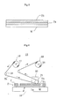
- Fig. 1 is a front view showing an outline of a tape applying apparatus.
- Figs. 2 through 4 are schematic front views illustrating a protective tape applying process.
- An apparatus 1 for applying protective tape to semiconductor wafers has a tape server 2 for supplying protective tape T1 along with a separator S, a separator collector 5 for separating and collecting the separator S from the protective tape T1, a chuck table 7 for suction-supporting a semiconductor wafer W (hereinafter simply called "wafer W") thereon, a tape applying mechanism 8 for pressing and applying the protective tape T1 to the wafer W, a cutter unit 10 for cutting the protective tape T1 on the wafer W along the circumference of the wafer W, a tape separating mechanism 11 for separating residual tape T2 from the wafer W, and a tape collector 13 for collecting the separated tape.
- a tape server 2 for supplying protective tape T1 along with a separator S
- a separator collector 5 for separating and collecting the separator S from the protective tape T1
- a chuck table 7 for suction-supporting a semiconductor wafer W (hereinafter simply called "wafer W") thereon
- a tape applying mechanism 8 for
- the tape server 2 guides the protective tape T1 with separator S in a strip form drawn from a tape bobbin 3 to move around a group of guide rollers 4 in a winding manner.
- the tape bobbin 3 is supported by a vertical wall, not shown, and is checked against rotation by a braking mechanism or the like.
- the separator collector 5 has a collecting bobbin 6 supported by the vertical wall not shown, and is operatively connected to a driving device such as a motor.
- the chuck table 7 has guide pins for adjusting position of the wafer W placed thereon with reference to an orientation flat of the wafer, while suction supporting the wafer at the back surface thereof.
- the tape applying mechanism 8 has a frame thereof held by a rail of a main body of the apparatus and operatively connected to a driving device such as a motor not shown, to be slidable in a tape running direction.
- the frame rotatably supports an applicator roller 9 which is vertically swung by a cylinder or the like not shown.
- the applicator roller 9 applies the protective tape T1 to the surface of the wafer W while pressing and rolling on the surface of the protective tape T1.
- the cutter unit 10 is vertically movable by a lift mechanism, not shown, between a standby position and a cutting position for cutting the protective tape T1.
- the cutter unit 10 cuts the protective tape T1 along the circumference of the wafer W.
- the tape separating mechanism 11 has a frame thereof held by the rail of the main body of the apparatus and operatively connected to a driving device such as a motor not shown, to be slidable in the tape running direction.
- the frame rotatably supports a separator roller 12 which is vertically swung by a cylinder or the like not shown.
- the separator roller 12 is provided to separate from the wafer W the residual tape T2 which is left thereon after the tape is cut along the circumference of the wafer W.
- the tape collector 13 has a collecting bobbin 14 supported by the vertical wall not shown, and is operatively connected to a driving device such as a motor. That is, a predetermined quantity of protective tape T1 is drawn from the tape server 2 and fed onto the wafer W.
- the collecting bobbin 14 is driven by the driving device to wind up the residual tape T2 left after a cutting operation.
- a method of applying protective tape in a plurality of plies which is the characterizing feature of this embodiment, will be described with reference to the drawings, using the tape applying apparatus having the above construction.
- two tape applying apparatus are used to apply two different types of protective tape in a plurality of plies to the surface of each wafer.
- the two types of protective tape used in this embodiment are, for example, a soft substrate with a tensile modulus of 30 to 100 MPa and a hard substrate with a tensile modulus of 100 to 1000 Mpa, both coated with an adhesive.
- the tensile modulus has been measured, using samples of 1cm 2 , at a tension speed of 50mm/min and in an environment of 23°C.
- a first and a second tape applying apparatus are arranged side by side.
- a soft protective tape T1 is set on the tape bobbin 3 of the first tape applying apparatus and a hard protective tape T3 is set on the tape bobbin 3 of the second tape applying apparatus.
- a wafer W is placed on, positionally adjusted to and suction-supported by the chuck table 7 of the first tape applying apparatus.
- the tape applying mechanism 8 and tape separating mechanism 11 are in an initial position at the left side, and the cutter unit 10 in the upper standby position.
- the applicator roller 9 of the tape applying mechanism 8 is swung downward. Then the applicator roller 9 rolls in a direction opposite to the tape running direction (from left to right in Fig. 2.) while pressing down the protective tape T1. In this way, the protective tape T1 is applied uniformly over the surface of the wafer W.
- the applicator roller 9 is raised.
- the cutter unit 10 is lowered to the cutting position to cut the protective tape T1.
- the cutter unit 10 is turned to make a complete circle circumferentially of the wafer W, thereby cutting out the protective tape T1 around the wafer W.
- the cutter unit 10 After cutting out the protective tape T1, the cutter unit 10 is raised back to the standby position as shown in Fig. 4.
- the tape separating mechanism 11 takes up and separates the residual tape T2 left on the wafer W while moving over the wafer W in the direction opposite to the tape running direction.
- the tape separating mechanism 11 When the tape separating mechanism 11 reaches a terminal position for the separating operation, the tape separating mechanism 11 and the tape applying mechanism 8 are moved in the tape running direction back to the initial position shown in Fig. 1. In the meantime, the residual tape T2 is rolled up by the collecting bobbin 14, while a predetermined quantity of tape is drawn from the tape server 2. This ends the operation for applying the protective tape T1 to the surface of the wafer W in the first tape applying apparatus.
- the wafer W, with the protective tape T1 applied to the surface thereof in the first tape applying apparatus, is transferred to the second tape applying apparatus.
- an adjustment is made to apply the second protective tape T3 in a direction turned 90 degrees relative to the direction of applying the first protective tape T1.
- Protective tapes may be applied in a number of different combinations, e.g. a soft tape and a hard tape applied in the stated order to the surface of wafer W, a hard tape and a soft tape applied in this order, tapes of the same type, or a UV curable tape and a non-UV curable tape.
- the number of tapes applied is not limited to two, but may be more than two.
- UV curable tape and a non-UV curable tape among the above combinations of protective tapes
- a UV irradiation of the protective tapes will ease separation of the UV curable tape, thus reducing the tensile force applied to the wafer on separation of this tape.
- each protective tape may easily be stretched in the tape applying direction when the applicator roller 9 rolls and presses on the protective tape. This reduces excessive stress acting on the wafer W in time of pressing and stretching the protective tapes applied to the wafer W.
- the soft protective tape T1 By applying the soft protective tape T1 to the surface of wafer W, irregularities on the surface of the wafer W are absorbed to render the surface level and smooth. As a result, the protective tape T3 may be applied uniformly over the first protective tape T1.
- the second protective tape T3 is applied in a direction turned 90 degrees relative to the applying direction of the first protective tape T1. This is effective to correct a warp of the wafer caused by the tension acting in the tape applying direction when the first protective tape T1 is applied.
- Fig. 6 is a front view showing an outline of a tape separating apparatus.
- Figs. 7 through 9 are schematic front views illustrating a protective tape separating process.
- An apparatus 15 for separating protective tape from semiconductor wafers has a tape server 16 for supplying a separating tape Ts, a chuck table 19 for suction-supporting a wafer W supported at the back surface thereof by a ring frame f through an adhesive tape Tn (hereinafter simply called "mount frame F"), a separating mechanism 20 for pressing and applying the separating tape Ts to the protective tape T3 applied over the surface of the wafer W and separating the separating tape Ts together with the protective tape T3, and a tape collector 22 for collecting both tapes separated from the wafer W.
- a tape server 16 for supplying a separating tape Ts
- a chuck table 19 for suction-supporting a wafer W supported at the back surface thereof by a ring frame f through an adhesive tape Tn (hereinafter simply called "mount frame F")
- a separating mechanism 20 for pressing and applying the separating tape Ts to the protective tape T3 applied over the surface of the wafer W and separating the separating tape Ts together
- the tape server 16 guides the separating tape Ts drawn from a tape bobbin 17 to the separating mechanism 20 by way of a guide roller 18.
- the tape bobbin 17 is supported by a vertical wall not shown.
- the chuck table 19 has guide pins for adjusting position of the mount frame F transferred thereto.
- the chuck table 19 is constructed to suck the back surface of the mount frame F. Further, the chuck table 19 has a frame thereof held by a rail of a main body of the apparatus and operatively connected to a driving device such as a motor not shown, to be slidable in a running direction of the separating tape Ts.
- the separating mechanism 20 has a separator roller 21 rotatably supported by a frame thereof and vertically swung by a cylinder or the like not shown.
- the separator roller 21 is operable to press and apply the separating tape Ts to the surface of the protective tape T3.
- the tape collector 22 has a collecting bobbin 23 supported by the vertical wall not shown, and operatively connected to a driving device not shown. That is, a predetermined quantity of separating tape Ts is drawn from the tape server 16 and fed onto the wafer W.
- the collecting bobbin 23 is driven by the driving device to wind up the separating tape Ts joined with the protective tape T3.
- a mount frame F is placed on the chuck table 19, the mount frame F having a wafer W with two protective tapes T1 and T3 of different hardness levels applied thereto, the wafer W being supported at the back surface thereof by a ring frame f through an adhesive tape.
- the position of the mount frame F is adjusted, which is then suction-supported by the chuck table 19.
- the chuck table 19 is moved (leftward in Fig. 7) to a position having the separator roller 21 in contact with a peripheral portion of the wafer W.
- the separator roller 21 is swung down and the chuck table 19 is moved in the running direction of the separating tape Ts. With the movement of the chuck table 19, the separator roller 21 rolls over the wafer W pressing the separating tape Ts thereon. That is, the separating tape Ts is applied to the uppermost protective tape T3, and the protective tape T3 with the separating tape Ts adhering thereto is taken up and separated together with the separating tape Ts.
- the orientation of the mount frame F on the chuck table 19 is changed.
- the mount frame F may be turned 90 degrees relative to the direction of separating the protective tape T3, or may be turned so that the protective tape T1 is separated along any one of cross recesses in the patterned surface of the wafer W.
- the protective tape T1 is separated from the surface of wafer W by repeating the same operation for separating the protective tape T3.
- each protective tape is treated to prevent the tapes from sticking hard to each other when wound into a roll.
- the protective tapes are easily separated one by one starting with the uppermost tape.
- the above method requires a relatively small pulling force for separating the protective tapes from the surface of wafer W, one by one starting from the uppermost tape. That is, the wafer W undergoes a reduced stress due to the tensile force of the tapes occurring in time of separating the tapes.
- the adhesive may be removed altogether from the recess.
Landscapes
- Container, Conveyance, Adherence, Positioning, Of Wafer (AREA)
- Mechanical Treatment Of Semiconductor (AREA)
- Processing Of Stones Or Stones Resemblance Materials (AREA)
- Sheets, Magazines, And Separation Thereof (AREA)
- Dicing (AREA)
Abstract
Description
Claims (15)
- A method of applying protective tapes to a surface of a semiconductor wafer with a pattern formed thereon, said method comprising:a step of applying the protective tapes to the surface of the wafer by repeating a process of applying each of said protective tapes.
- A method of applying protective tapes as defined in claim 1, wherein said protective tapes applied in a plurality of plies to the surface of the wafer are progressively harder upward away from the surface.
- A method of applying protective tapes as defined in claim 1, wherein the protective tapes applied in a plurality of plies to the surface of the wafer comprise a UV curable tape applied to the surface of the wafer, and a non-UV curable tape applied to said UV curable tape.
- A method of applying protective tapes as defined in claim 1, wherein said protective tapes applied in a plurality of plies to the surface of the wafer are progressively softer upward away from the surface.
- A method of applying protective tapes as defined in claim 1, wherein the protective tapes applied in a plurality of plies to the surface of the wafer comprise protective tapes of the same type.
- A method of applying protective tapes as defined in claim 1, wherein each of said protective tapes is applied in a different direction.
- A method of applying protective tapes as defined in claim 6, wherein the protective tapes are applied such that, after a first protective tape is applied to the surface of the wafer in a first direction, a next protective tape is applied in a direction perpendicular to said first direction.
- A method of applying protective tapes as defined in claim 1, wherein a plurality of tape applying apparatus are used to apply the protective tapes to the surface of the wafer by repeating the process of applying each of said protective tapes.
- A method of applying protective tapes as defined in claim 1, wherein one tape applying apparatus is used to apply the protective tapes to the surface of the wafer by repeating the process of applying each of said protective tapes.
- A method of applying protective tapes as defined in claim 1, wherein the protective tapes applied to the surface of the wafer are in a strip form and are each cut substantially circumferentially of the wafer upon application to the surface of the wafer.
- A method of applying protective tapes as defined in claim 1, wherein the protective tapes applied to the surface of the wafer are in a label form cut in advance substantially circumferentially of the wafer.
- A method of separating a plurality of protective tapes applied to a surface of a semiconductor wafer with a pattern formed thereon, said method comprising:a step of individually separating the plurality of protective tapes in plural times starting with an uppermost tape.
- A method of separating protective tapes as defined in claim 12, wherein the plurality of protective tapes are separated such that, after a first protective tape is separated in a first direction, a next protective tape is separated in a direction perpendicular to said first direction.
- A method of separating protective tapes as defined in claim 12, wherein the plurality of protective tapes are separated by varying separating directions in accordance with the pattern on the surface.
- A method of separating protective tapes as defined in claim 14, wherein the plurality of protective tapes are separated along recesses formed in the pattern on the surface.
Applications Claiming Priority (2)
| Application Number | Priority Date | Filing Date | Title |
|---|---|---|---|
| JP2001307411A JP3770820B2 (en) | 2001-10-03 | 2001-10-03 | How to apply the protective tape |
| JP2001307411 | 2001-10-03 |
Publications (2)
| Publication Number | Publication Date |
|---|---|
| EP1300873A2 true EP1300873A2 (en) | 2003-04-09 |
| EP1300873A3 EP1300873A3 (en) | 2004-05-12 |
Family
ID=19126877
Family Applications (1)
| Application Number | Title | Priority Date | Filing Date |
|---|---|---|---|
| EP02021889A Withdrawn EP1300873A3 (en) | 2001-10-03 | 2002-09-30 | Methods of applying and separating protective tapes |
Country Status (7)
| Country | Link |
|---|---|
| US (1) | US6803320B2 (en) |
| EP (1) | EP1300873A3 (en) |
| JP (1) | JP3770820B2 (en) |
| KR (1) | KR100915259B1 (en) |
| CN (1) | CN1293610C (en) |
| SG (1) | SG111084A1 (en) |
| TW (1) | TW591692B (en) |
Cited By (1)
| Publication number | Priority date | Publication date | Assignee | Title |
|---|---|---|---|---|
| EP4406890A1 (en) * | 2023-01-24 | 2024-07-31 | MKE Metall- und Kunststoffwaren Erzeugungsgesellschaft m.b.H. | Device, arrangement and method for automatically detaching a thermally conductive pad from a carrier film |
Families Citing this family (36)
| Publication number | Priority date | Publication date | Assignee | Title |
|---|---|---|---|---|
| JP2003209082A (en) * | 2002-01-15 | 2003-07-25 | Nitto Denko Corp | Method and device for attaching protective tape and method for removing protective tape |
| JP4318471B2 (en) * | 2003-03-05 | 2009-08-26 | 日東電工株式会社 | How to apply and peel off protective tape |
| US20060194412A1 (en) * | 2004-04-07 | 2006-08-31 | Takehito Nakayama | Method and device for sticking tape |
| JP2005019518A (en) * | 2003-06-24 | 2005-01-20 | Nitto Denko Corp | Protective sheet for semiconductor wafer processing and backside grinding method of semiconductor wafer |
| JP2005014184A (en) * | 2003-06-27 | 2005-01-20 | Nitto Denko Corp | Method of cutting ultraviolet curable adhesive tape and article formed using the same |
| JP4666565B2 (en) * | 2003-10-06 | 2011-04-06 | 日東電工株式会社 | Protective sheet for processing semiconductor wafer and method for grinding back surface of semiconductor wafer |
| JP4489414B2 (en) * | 2003-11-26 | 2010-06-23 | 株式会社 日立ディスプレイズ | Display device manufacturing method and manufacturing apparatus thereof |
| JP4472316B2 (en) * | 2003-11-28 | 2010-06-02 | 日東電工株式会社 | Adhesive tape cutting method and adhesive tape cutting device |
| JP4584607B2 (en) * | 2004-03-16 | 2010-11-24 | 浜松ホトニクス株式会社 | Processing object cutting method |
| TW200539357A (en) * | 2004-04-28 | 2005-12-01 | Lintec Corp | Adhering apparatus and adhering method |
| JP4550510B2 (en) * | 2004-07-27 | 2010-09-22 | リンテック株式会社 | Sheet peeling apparatus and peeling method |
| JP4540403B2 (en) | 2004-06-16 | 2010-09-08 | 株式会社東京精密 | Tape sticking method and tape sticking apparatus |
| JP4387879B2 (en) * | 2004-06-17 | 2009-12-24 | 株式会社ディスコ | Protective tape mounting method and protective tape mounting apparatus |
| JP2006024676A (en) * | 2004-07-07 | 2006-01-26 | Disco Abrasive Syst Ltd | Wafer division method |
| JP4507826B2 (en) * | 2004-10-27 | 2010-07-21 | 日東電工株式会社 | Protective sheet for processing semiconductor wafer and method for grinding back surface of semiconductor wafer |
| JP4326519B2 (en) * | 2005-03-31 | 2009-09-09 | 日東電工株式会社 | Protective tape peeling method and apparatus using the same |
| JP4401322B2 (en) * | 2005-04-18 | 2010-01-20 | 日東電工株式会社 | Support plate separation apparatus and support plate separation method using the same |
| JP4795772B2 (en) * | 2005-10-24 | 2011-10-19 | リンテック株式会社 | Sheet cutting table and sheet sticking apparatus |
| JP4836557B2 (en) * | 2005-11-25 | 2011-12-14 | 株式会社東京精密 | Dicing tape sticking device and dicing tape sticking method |
| JP4953764B2 (en) * | 2005-11-29 | 2012-06-13 | 株式会社東京精密 | Peeling tape sticking method and peeling tape sticking device |
| JP4745945B2 (en) * | 2006-12-04 | 2011-08-10 | リンテック株式会社 | Conveying device, sheet sticking device using the same, and sheet peeling device |
| JP5216472B2 (en) * | 2008-08-12 | 2013-06-19 | 日東電工株式会社 | Method and apparatus for attaching protective tape to semiconductor wafer |
| JP5324317B2 (en) * | 2009-05-22 | 2013-10-23 | 日東電工株式会社 | Protective tape application method and protective tape application device |
| US8574398B2 (en) | 2010-05-27 | 2013-11-05 | Suss Microtec Lithography, Gmbh | Apparatus and method for detaping an adhesive layer from the surface of ultra thin wafers |
| JP6328874B2 (en) * | 2012-07-18 | 2018-05-23 | リンテック株式会社 | Sheet pasting apparatus and method for preventing enlargement of apparatus |
| JP5589045B2 (en) * | 2012-10-23 | 2014-09-10 | 日東電工株式会社 | Semiconductor wafer mounting method and semiconductor wafer mounting apparatus |
| KR101447578B1 (en) * | 2012-12-27 | 2014-10-06 | 한국미쯔보시다이아몬드공업(주) | Apparatus for removing cullet generated when dividing brittle material substrate |
| KR101447577B1 (en) * | 2012-12-27 | 2014-10-08 | 한국미쯔보시다이아몬드공업(주) | Apparatus for removing cullet generated when scribing brittle material substrate |
| CN104347449A (en) * | 2013-07-24 | 2015-02-11 | 上海和辉光电有限公司 | A peeling device and peeling method |
| JP6219196B2 (en) * | 2014-02-26 | 2017-10-25 | リンテック株式会社 | Sheet sticking method and sticking device |
| CN107742575A (en) * | 2017-10-10 | 2018-02-27 | 深圳市信维通信股份有限公司 | A kind of preparation method and manufacture system of amorphous or nanocrystalline strip lamination |
| EP3546952B1 (en) * | 2018-03-26 | 2024-03-06 | Roche Diagnostics GmbH | Method for unsealing an opening of a laboratory sample container, method for handling a laboratory sample container, laboratory apparatus and laboratory automation system |
| US11889742B2 (en) * | 2020-11-04 | 2024-01-30 | Samsung Display Co., Ltd. | Apparatus of manufacturing display device and method of manufacturing display device |
| JP7625434B2 (en) * | 2021-02-05 | 2025-02-03 | 株式会社東京精密 | Tape application device |
| JP7737821B2 (en) * | 2021-06-04 | 2025-09-11 | リンテック株式会社 | Sheet pasting device and sheet pasting method |
| JP7778515B2 (en) * | 2021-09-30 | 2025-12-02 | 株式会社ディスコ | How to divide the workpiece |
Family Cites Families (20)
| Publication number | Priority date | Publication date | Assignee | Title |
|---|---|---|---|---|
| US3181988A (en) * | 1961-01-03 | 1965-05-04 | Kleen Stik Products Inc | Tape applying machine |
| US5203143A (en) * | 1992-03-28 | 1993-04-20 | Tempo G | Multiple and split pressure sensitive adhesive stratums for carrier tape packaging system |
| US5480842A (en) * | 1994-04-11 | 1996-01-02 | At&T Corp. | Method for fabricating thin, strong, and flexible die for smart cards |
| CN2199596Y (en) * | 1994-07-25 | 1995-05-31 | 赵广文 | Silicon single wafer tape attaching device |
| KR19990028523A (en) * | 1995-08-31 | 1999-04-15 | 야마모토 히데키 | Method for peeling protective adhesive tape of semiconductor wafer and its device |
| KR970030225A (en) * | 1995-11-08 | 1997-06-26 | 김광호 | Manufacturing method of semiconductor small in which the backside of wafer is polished using UV tape |
| JP3535318B2 (en) * | 1996-09-30 | 2004-06-07 | 富士通株式会社 | Semiconductor device and manufacturing method thereof |
| JPH10116884A (en) * | 1996-10-11 | 1998-05-06 | Teikoku Seiki Kk | Wafer protection tape cutter |
| US5776799A (en) * | 1996-11-08 | 1998-07-07 | Samsung Electronics Co., Ltd. | Lead-on-chip type semiconductor chip package using an adhesive deposited on chip active surfaces at a wafer level and method for manufacturing same |
| JPH10337823A (en) * | 1997-04-11 | 1998-12-22 | Lintec Corp | Base material and pressure-sensitive adhesive tape using the base material |
| JP3759820B2 (en) * | 1997-05-30 | 2006-03-29 | リンテック株式会社 | Method and apparatus for attaching semiconductor wafer protective film |
| KR100249313B1 (en) * | 1997-07-25 | 2000-03-15 | 윤종용 | Tape laminating system for semiconductor device and its driving method |
| KR20000008966A (en) * | 1998-07-20 | 2000-02-15 | 윤종용 | Wafer sawing method using a protection tape |
| JP3560823B2 (en) * | 1998-08-18 | 2004-09-02 | リンテック株式会社 | Wafer transfer device |
| JP4149583B2 (en) * | 1998-09-10 | 2008-09-10 | 株式会社ディスコ | Grinding equipment |
| US6153536A (en) * | 1999-03-04 | 2000-11-28 | International Business Machines Corporation | Method for mounting wafer frame at back side grinding (BSG) tool |
| JP2000331968A (en) * | 1999-05-21 | 2000-11-30 | Tokyo Seimitsu Co Ltd | Wafer protection tape |
| JP2001021873A (en) * | 1999-07-07 | 2001-01-26 | Sony Corp | Manufacturing method of liquid crystal display device |
| US6245677B1 (en) * | 1999-07-28 | 2001-06-12 | Noor Haq | Backside chemical etching and polishing |
| US6352935B1 (en) * | 2000-01-18 | 2002-03-05 | Analog Devices, Inc. | Method of forming a cover cap for semiconductor wafer devices |
-
2001
- 2001-10-03 JP JP2001307411A patent/JP3770820B2/en not_active Expired - Fee Related
-
2002
- 2002-09-30 SG SG200205948A patent/SG111084A1/en unknown
- 2002-09-30 EP EP02021889A patent/EP1300873A3/en not_active Withdrawn
- 2002-10-02 TW TW091122685A patent/TW591692B/en not_active IP Right Cessation
- 2002-10-02 KR KR1020020060049A patent/KR100915259B1/en not_active Expired - Fee Related
- 2002-10-03 US US10/262,881 patent/US6803320B2/en not_active Expired - Fee Related
- 2002-10-08 CN CNB021442835A patent/CN1293610C/en not_active Expired - Fee Related
Cited By (1)
| Publication number | Priority date | Publication date | Assignee | Title |
|---|---|---|---|---|
| EP4406890A1 (en) * | 2023-01-24 | 2024-07-31 | MKE Metall- und Kunststoffwaren Erzeugungsgesellschaft m.b.H. | Device, arrangement and method for automatically detaching a thermally conductive pad from a carrier film |
Also Published As
| Publication number | Publication date |
|---|---|
| KR100915259B1 (en) | 2009-09-03 |
| JP3770820B2 (en) | 2006-04-26 |
| SG111084A1 (en) | 2005-05-30 |
| TW591692B (en) | 2004-06-11 |
| CN1293610C (en) | 2007-01-03 |
| JP2003115469A (en) | 2003-04-18 |
| US6803320B2 (en) | 2004-10-12 |
| CN1409380A (en) | 2003-04-09 |
| US20030064592A1 (en) | 2003-04-03 |
| EP1300873A3 (en) | 2004-05-12 |
| KR20030029469A (en) | 2003-04-14 |
Similar Documents
| Publication | Publication Date | Title |
|---|---|---|
| US6803320B2 (en) | Protective tape applying and separating methods | |
| US6919284B2 (en) | Protective tape applying method and apparatus, and protective tape separating method | |
| US6716295B2 (en) | Protective tape applying and separating method | |
| US10622230B2 (en) | Protective tape attaching method | |
| US7335605B2 (en) | Protective tape applying and separating method | |
| KR19990028523A (en) | Method for peeling protective adhesive tape of semiconductor wafer and its device | |
| WO2011013348A1 (en) | Method for adhering protection tape, and protection tape used in the method | |
| TWI795468B (en) | Method and apparatus for joining adhesive tape | |
| TWI257666B (en) | Method and apparatus for joining adhesive tape | |
| JP4334420B2 (en) | Protective tape application method and protective tape application device | |
| JP2005243700A (en) | Adhesive sheet pasting method and apparatus using the same | |
| JP2011114271A (en) | Bonding sheet for processing semiconductor wafer and method for processing semiconductor wafer employing the sheet | |
| JP2005340859A (en) | How to peel off the protective tape | |
| JPH0745559A (en) | Method of adhering adhesive tape to semiconductor wafer | |
| JP2004266183A (en) | Adhesive tape attaching method and its device |
Legal Events
| Date | Code | Title | Description |
|---|---|---|---|
| PUAI | Public reference made under article 153(3) epc to a published international application that has entered the european phase |
Free format text: ORIGINAL CODE: 0009012 |
|
| AK | Designated contracting states |
Kind code of ref document: A2 Designated state(s): AT BE BG CH CY CZ DE DK EE ES FI FR GB GR IE IT LI LU MC NL PT SE SK TR Designated state(s): AT BE BG CH CY CZ DE DK EE ES FI FR GB GR IE IT LI LU MC NL PT SE SK TR |
|
| AX | Request for extension of the european patent |
Extension state: AL LT LV MK RO SI |
|
| PUAL | Search report despatched |
Free format text: ORIGINAL CODE: 0009013 |
|
| AK | Designated contracting states |
Kind code of ref document: A3 Designated state(s): AT BE BG CH CY CZ DE DK EE ES FI FR GB GR IE IT LI LU MC NL PT SE SK TR |
|
| AX | Request for extension of the european patent |
Extension state: AL LT LV MK RO SI |
|
| 17P | Request for examination filed |
Effective date: 20040608 |
|
| AKX | Designation fees paid |
Designated state(s): AT BE BG CH CY CZ DE DK EE ES FI FR GB GR IE IT LI LU MC NL PT SE SK TR |
|
| STAA | Information on the status of an ep patent application or granted ep patent |
Free format text: STATUS: THE APPLICATION IS DEEMED TO BE WITHDRAWN |
|
| 18D | Application deemed to be withdrawn |
Effective date: 20051206 |