EP1300711A2 - Semiconductor device for optically coupling semiconductor light-emitting device to optical fiber - Google Patents
Semiconductor device for optically coupling semiconductor light-emitting device to optical fiber Download PDFInfo
- Publication number
- EP1300711A2 EP1300711A2 EP02021484A EP02021484A EP1300711A2 EP 1300711 A2 EP1300711 A2 EP 1300711A2 EP 02021484 A EP02021484 A EP 02021484A EP 02021484 A EP02021484 A EP 02021484A EP 1300711 A2 EP1300711 A2 EP 1300711A2
- Authority
- EP
- European Patent Office
- Prior art keywords
- shell
- stress
- semiconductor device
- reinforcement
- lens
- Prior art date
- Legal status (The legal status is an assumption and is not a legal conclusion. Google has not performed a legal analysis and makes no representation as to the accuracy of the status listed.)
- Granted
Links
Images




Classifications
-
- G—PHYSICS
- G02—OPTICS
- G02B—OPTICAL ELEMENTS, SYSTEMS OR APPARATUS
- G02B7/00—Mountings, adjusting means, or light-tight connections, for optical elements
- G02B7/02—Mountings, adjusting means, or light-tight connections, for optical elements for lenses
- G02B7/027—Mountings, adjusting means, or light-tight connections, for optical elements for lenses the lens being in the form of a sphere or ball
-
- G—PHYSICS
- G02—OPTICS
- G02B—OPTICAL ELEMENTS, SYSTEMS OR APPARATUS
- G02B6/00—Light guides; Structural details of arrangements comprising light guides and other optical elements, e.g. couplings
- G02B6/24—Coupling light guides
- G02B6/42—Coupling light guides with opto-electronic elements
- G02B6/4201—Packages, e.g. shape, construction, internal or external details
-
- G—PHYSICS
- G02—OPTICS
- G02B—OPTICAL ELEMENTS, SYSTEMS OR APPARATUS
- G02B6/00—Light guides; Structural details of arrangements comprising light guides and other optical elements, e.g. couplings
- G02B6/24—Coupling light guides
- G02B6/42—Coupling light guides with opto-electronic elements
- G02B6/4201—Packages, e.g. shape, construction, internal or external details
- G02B6/4204—Packages, e.g. shape, construction, internal or external details the coupling comprising intermediate optical elements, e.g. lenses, holograms
-
- G—PHYSICS
- G02—OPTICS
- G02B—OPTICAL ELEMENTS, SYSTEMS OR APPARATUS
- G02B6/00—Light guides; Structural details of arrangements comprising light guides and other optical elements, e.g. couplings
- G02B6/24—Coupling light guides
- G02B6/42—Coupling light guides with opto-electronic elements
- G02B6/4201—Packages, e.g. shape, construction, internal or external details
- G02B6/4219—Mechanical fixtures for holding or positioning the elements relative to each other in the couplings; Alignment methods for the elements, e.g. measuring or observing methods especially used therefor
- G02B6/4236—Fixing or mounting methods of the aligned elements
- G02B6/4237—Welding
-
- G—PHYSICS
- G02—OPTICS
- G02B—OPTICAL ELEMENTS, SYSTEMS OR APPARATUS
- G02B6/00—Light guides; Structural details of arrangements comprising light guides and other optical elements, e.g. couplings
- G02B6/24—Coupling light guides
- G02B6/42—Coupling light guides with opto-electronic elements
- G02B6/4201—Packages, e.g. shape, construction, internal or external details
- G02B6/4266—Thermal aspects, temperature control or temperature monitoring
- G02B6/4267—Reduction of thermal stress, e.g. by selecting thermal coefficient of materials
-
- G—PHYSICS
- G02—OPTICS
- G02B—OPTICAL ELEMENTS, SYSTEMS OR APPARATUS
- G02B6/00—Light guides; Structural details of arrangements comprising light guides and other optical elements, e.g. couplings
- G02B6/24—Coupling light guides
- G02B6/42—Coupling light guides with opto-electronic elements
- G02B6/4201—Packages, e.g. shape, construction, internal or external details
- G02B6/4266—Thermal aspects, temperature control or temperature monitoring
- G02B6/4268—Cooling
Definitions
- the invention relates to a semiconductor device for optically coupling a semiconductor light-emitting device to an optical fiber.
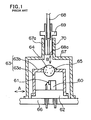
- FIG. 1 is a cross-sectional view of a semiconductor laser module including such a semiconductor device, disclosed in Japanese Patent Publication No. 3-61927, as an example.
- the semiconductor device for optically coupling a semiconductor light-emitting device to an optical fiber is comprised of a spherical-lens holder 63 fixedly mounted on a stem 62 on which a heat sink 60 to which a semiconductor laser device 61 is fixed is mounted, a spherical lens 64 fit into a hole formed centrally with the spherical-lens holder 63 such that a center of the spherical lens 64 is on an extension of an optical axis of the semiconductor laser device 61, and wax 65 coated in a belt around the spherical-lens holder 63 to keep inside of the spherical-lens holder 63 in air-tight condition.
- the spherical-lens holder 63 is comprised of a first portion 63 formed cylindrical, and a second portion 63a formed annular, formed integral with the first portion 63a at an upper end of the first portion 63a, and formed centrally with a hole into which the spherical lens 64 is fit.
- the semiconductor device for optically coupling a semiconductor light-emitting device to an optical fiber cooperates with other parts to thereby define a semiconductor laser module. Positional relations between the semiconductor device and other parts are as follows.
- a ferrule holder 67 which surrounds the spherical-lens holder 63 therein.
- the ferrule holder 67 is formed with a projecting tube 67a into which a ferrule 69 to which an optical fiber 68 is physically connected is inserted.
- the ferrule holder 67 is adjusted in position in a direction A perpendicular to an optical axis with the ferrule holder 67 being mounted on the base 66, and further, the ferrule 69 is slid in the projecting tube 67a in a direction B of an optical axis such that laser beams emitted from the semiconductor laser device 61 through the spherical lens 64 are focused on an end surface 68a of the optical fiber 68.
- the ferrule holder 67 is fixed on the base 66 by resistance welding.
- the ferrule 69 is fixed to the ferrule holder 67 by adhesive 70.
- the spherical lens 64 is supported on the spherical-lens holder 63 through the wax 65 in the conventional semiconductor device for optically coupling a semiconductor light-emitting device to an optical fiber, illustrated in FIG. 1, the spherical lens 64 is generally supported on the spherical-lens holder 63 through glass having a low fusing point, in order to more certainly keep the spherical lens 64 and the spherical-lens holder 63 hermetically sealed therebetween.
- the spherical-lens holder 63 is fixed to the stem by resistance welding. In such resistance welding, a temperature of about 1,400 degrees centigrade is applied instantaneously to the spherical-lens holder 63.
- a lower portion of the first portion 63a of the spherical-lens holder 63 is heated to a temperature of about 1,400 degrees centigrade, but since a temperature of about 1,400 degrees centigrade is applied to the spherical-lens holder 63 for quite a short period of time, an upper portion of the first portion 63a, for instance, a portion at which the first portion 63a and the second portion 63b are connected to each other is heated only to about 30 to 40 degrees centigrade.
- the first portion 63a expands to a greater degree at a lower portion thereof than at an upper portion thereof.
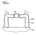
- a thermal stress in the spherical-lens holder 63 As illustrated in FIG. 2, the thermal stress acts on the spherical-lens holder 63 as a compressive stress T directing towards a center from an outer edge of the spherical-lens holder 63.
- the compressive stress T causes elastic deformation in the spherical-lens holder 63, as shown in FIG. 2 with a broken line 63c.
- an interface between the spherical lens 64 and the spherical-lens holder 63 in other words, the wax 65 or the glass has the smallest resistance to a stress among parts constituting the semiconductor device. Accordingly, when the spherical-lens holder 63 is elastically deformed as shown in FIG. 2 with the broken line 63c, a stress caused by the elastic deformation acts on the wax 65 or the glass most.
- the wax 65 or the glass is cracked. If the crack reaches both inner and outer surfaces of the spherical-lens holder 63, there is generated a leakage path through which air enters from outside into inside of the spherical-lens holder 63. Thus, it is no longer possible to keep the spherical lens 64 and the spherical-lens holder 63 hermetically sealed therebetween, resulting in reduction in a light-emitting efficiency of the semiconductor laser device 61.
- a spherical-lens holder which is capable of preventing the wax 65 or the glass through which the spherical lens 64 and the spherical-lens holder 63 are hermetically sealed therebetween, from being cracked due to a thermal stress which is caused by heat generated when the spherical-lens holder 63 is fixed on the stem 62 by resistance welding.
- a semiconductor device for optically coupling a semiconductor light-emitting device to an optical fiber, including (a) a lens which focuses lights emitted from the semiconductor light-emitting device, onto the optical fiber, (b) a shell which supports the lens therewith and which is comprised of a cylindrical first portion, and a second portion integral with the first portion at an upper end of the first portion and being formed centrally with an opening into which the lens is to be fit, and (c) glass arranged around the lens for keeping the lens and the opening hermetically sealed, characterized by a stress eliminator which eliminates a stress acting on the shell when the shell is fixed onto a base by resistance welding, and prevents the shell from being elastically deformed due to the stress.
- the stress eliminator is comprised of a cylindrical third portion extending from the first portion upwardly beyond the second portion, and a reinforcement formed on at least one of upper and lower surfaces of the second portion.
- the inventor has found out that it was possible to a high degree to prevent a shell, which corresponds the spherical-lens holder 63 in the conventional semiconductor device illustrated in FIG. 1, from being elastically deformed due to a thermal stress caused by heat which was generated when the shell is fixed on a stem by resistance welding, by designing the shell to have a shape taking a thermal stress into consideration. Specifically, it is possible to increase a strength of the shell against a stress by providing a reinforcement on an upper or lower surface or on upper and lower surfaces of the second portion of the shell, and hence, it is possible to prevent the shell from being elastically deformed to a high degree. Accordingly, it is possible to prevent the glass from being cracked.
- the reinforcement is provided on an upper surface of the second portion of the shell, it is preferable to form the reinforcement integral with the third portion formed as an extension of the first portion, ensuring a further increased strength of the shell and further preventing the glass from being cracked.
- the reinforcement prefferably has a shape for covering a stress acting on the second portion therewith when thermal stress acts on the shell.
- the reinforcement By designing the reinforcement to entirely cover therewith a stress acting on the second portion, it would be possible to cancel a stress acting on the shell, with the reinforcement having a minimum area.
- the reinforcement may be designed to have various shapes.
- the reinforcement may be designed to have a linearly tapered cross-section.
- the reinforcement may be designed to have a step-shaped cross-section.
- the reinforcement may be designed to have an inwardly-projecting arcuate cross-section.
- the stress eliminator may be comprised of a stress-concentration portion formed with the second portion of the shell which stress-concentration portion has a thickness smaller than a thickness of the rest of the second portion and to which, when a stress acts on the shell, the stress is concentrated.
- the shell may be designed to have a stress-concentration portion in the second portion which stress-concentration portion has a thickness smaller than a thickness of the rest of the second portion. Since the stress-concentration portion has a strength smaller than a strength of the rest of the second portion, when the shell is elastically deformed due to a thermal stress, a stress caused by the elastic deformation of the shell is concentrated to and absorbed into the stress-concentration portion. Accordingly, it is possible to prevent a stress caused by the elastic deformation of the shell from acting on the glass defining an interface between the lens and the shell, and further prevent the glass from being cracked.
- the stress-concentration portion may be formed in various manners.
- the stress-concentration portion may be defined by one or more recess(es) extending from at least one of upper and lower surfaces of the second portion.
- the above-mentioned semiconductor devices may be applied to a semiconductor laser module.
- the reinforcement formed on an upper or lower surface or upper and lower surfaces of the second portion compensate for a stress acting on the second portion when the shell is elastically deformed. Accordingly, it is possible to prevent a shell from being elastically deformed to a high degree, when the shell is fixed on a stem by resistance welding. Hence, it is possible to prevent the glass from being cracked due to the elastic deformation of the shell.
- the reinforcement When the reinforcement is provided on an upper surface of the second portion of the shell, it is preferable to form the reinforcement integral with the third portion formed as an extension of the first portion, ensuring an increased strength of the reinforcement and further preventing the glass from being cracked.
- the shell By designing the shell to have a stress-concentration portion in the second portion which stress-concentration portion has a thickness smaller than a thickness of the rest of the second portion, when the shell is elastically deformed due to a thermal stress, a stress caused by the elastic deformation of the shell is concentrated to and absorbed into the stress-concentration portion. As a result, it is possible to prevent a stress caused by the elastic deformation of the shell from acting on the glass defining an interface between the lens and the shell, and hence, it is also possible to prevent the glass from being cracked.
- a semiconductor laser module to which the semiconductor devices in accordance with the embodiments of the present invention are applied has the same structure as the structure of the semiconductor laser module illustrated in FIG. 1 except the semiconductor device for optically coupling a semiconductor light-emitting device to an optical fiber.
- FIG. 3 illustrates a profile of a stress acting on a first portion 1b of a shell 1, which corresponds to the spherical-lens holder 63 illustrated in FIG. 1, which stress is generated when the shell 1 is elastically deformed due to heat generated when the shell 1 is fixed to a stem by resistance welding.
- the inventor analyzed a stress acting on the shell 1 when the shell 1 was elastically deformed. As a result of the analysis, it was found out that a stress acting on a second portion 1b of the shell 1 had such a linear tapered profile that it was greater at a position closer to the first portion 1a, and smaller at a position closer to a spherical lens 3, as illustrated in FIG. 3.
- a reinforcement to be formed on the second portion 1b of the shell 1 had to have such a shape as partially or entirely covering a stress acting on the second portion 1b.
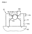
- FIG. 4 is a longitudinal cross-sectional view of a semiconductor device 10 for optically coupling a semiconductor light-emitting device to an optical fiber, in accordance with the first embodiment of the present invention.
- the semiconductor device 10 is comprised of a lens 11 which focuses lights emitted from a semiconductor light-emitting device, onto an optical fiber, a shell 12 which supports the lens 11 therewith, and a glass 13 arranged around the lens 11 for keeping the lens 11 and a later-mentioned opening 12d hermetically sealed to each other.
- the glass 13 is a glass having a low fusing point.
- the shell 12 is composed of 50 Fe/Ni, and is comprised of a cylindrical first portion 12a, an annular second portion 12b inwardly integral with the first portion 12a at an upper end of the first portion 12a and formed centrally with an opening 12d into which the lens 11 is to be fit, and a cylindrical third portion 12c extending from the first portion 12a upwardly beyond the second portion 12b.
- the semiconductor device 10 is comprised further of first and second reinforcements 14a and 14b formed on upper and lower surfaces of the second portion 12b of the shell, respectively.
- the first and second reinforcements 14a and 14b are annular, and have a linear cross-section which is tapered to the second portion 12b. In other words, a right-angled triangular cross-section in which two sides sandwiching a right angle therebetween make contact with the second and third portions 12b and 12c.
- the first and second reinforcements 14a and 14b are designed to have dimensions for entirely covering therewith a stress acting on the second portion 12b.
- the semiconductor device 10 is designed to include the third portion 12c formed as an extension of the first portion 12a upwardly beyond the second portion 12b.
- the first reinforcement 14a integral with the third portion 12c, it would be possible to significantly enhance a strength of the first reinforcement 14a, and hence, possible to further certainly prevent the glass 13 from being cracked.
- a current at which the spherical-lens holder 63 was fixed to the stem 62 by resistance welding in the conventional semiconductor device illustrated in FIG. 1 was in the range of 4.1 to 4.3 kA, whereas the same in the semiconductor device 10 in accordance with the first embodiment was in the range of 3.5 to 5.0 kA.
- the semiconductor device 10 can increase a range of a current at which the shell 12 is fixed to the stem 62 by resistance welding, up to 1.5 kA (5.0 - 3.5 kA) from 0.2 kA (4.3 - 4.1 kA).
- a spherical lens is used as the lens 11, but a shape of the lens 11 is not to be limited to a sphere.
- a non-spherical lens may be used as the lens 11. Any lens may be used as the lens 11 in the semiconductor device 10, if it has at least partially a circular arc in its surface.
- first and second reinforcements 14a and 14b are both formed on the upper and lower surfaces of the second portion 12b, it is not always necessary to form both the first and second reinforcements 14a and 14b on the second portion 12b.
- One of the first and second reinforcements 14a and 14b may be formed on the second portion 12b, in which case, the shell 12 would have an enhanced strength to a smaller degree than a case in which both the first and second reinforcements 14a and 14b are formed on the upper and lower surfaces of the second portion 12b, but the shell 12 could have a strength sufficient to prevent the elastic deformation of the shell 12.
- the inventor had measured a stress at a point X in FIG. 4, that is, an uppermost point in an interface between the lens 11 and the glass 13, as a typical stress caused by the elastic deformation of the shell 12.
- a compressive stress of 20.9 MPa was measured at the point X.
- the semiconductor device 10 can reduce a compressive stress by 31.7% relative to a compressive stress of 30.6 MPa in the conventional semiconductor device.
- the semiconductor device 10 can reduce a compressive stress by 30.1% relative to a compressive stress of 30.6 MPa in the conventional semiconductor device.
- the above-mentioned measurement shows that the semiconductor device 10 in accordance with the first embodiment can effectively reduce a stress by which the glass 13 will be cracked.
- FIG. 5 is a longitudinal cross-sectional view of a semiconductor device 20 for optically coupling a semiconductor light-emitting device to an optical fiber, in accordance with the second embodiment of the present invention.
- the shell 12 in the second embodiment is comprised of the first portion 12a, the second portion 12b and the second reinforcement 14b formed on the lower surface of the second portion 12b. That is, the shell 12 in the second embodiment is designed not to have the first reinforcement 14a and the third portion 12c in comparison with the semiconductor device 10 in accordance with the first embodiment, illustrated in FIG. 3.
- the first reinforcement 14a is not formed on the upper surface of the second portion 12b of the shell 12, it is not necessary to design the shell 12 to have the third portion 12c.
- the semiconductor device 20 since a stress acting on the lower surface of the second portion 12b when the shell 12 is elastically deformed is compensated for by the second reinforcement 14b formed on the lower surface of the second portion 12b, it is possible to prevent the shell 12 from being elastically deformed when the shell 12 is fixed on the stem 62 by resistance welding, though to a smaller degree than the semiconductor device 10 in accordance with the first embodiment. Accordingly, it is possible to prevent the glass 13 from being cracked due to the elastic deformation of the shell 12.
- FIG. 6 is a longitudinal cross-sectional view of a semiconductor device 30 for optically coupling a semiconductor light-emitting device to an optical fiber, in accordance with the third embodiment of the present invention.
- the semiconductor device 30 in accordance with the third embodiment is designed to include first and second step-shaped reinforcements 24a and 24b in place of the first and second reinforcements 14a and 14b in the first embodiment.
- the first and second step-shaped reinforcements 24a and 24b are 5 designed to have dimensions for entirely covering therewith a stress acting on the upper and lower surfaces of the second portion 12b. Accordingly, the semiconductor device 30 prevents the glass 13 from being cracked due to the elastic deformation of the shell 12, similarly to the semiconductor device 10 in accordance with the first embodiment.
- first and second step-shaped reinforcements 24a and 24b are not always necessary to form both the first and second step-shaped reinforcements 24a and 24b on the second portion 12b.
- One of the first and second step-shaped reinforcements 24a and 24b may be formed on the second portion 12b.
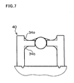
- FIG. 7 is a longitudinal cross-sectional view of a semiconductor device 40 for optically coupling a semiconductor light-emitting device to an optical fiber, in accordance with the fourth embodiment of the present invention.
- the semiconductor device 40 in accordance with the fourth embodiment is designed to include first and second reinforcements 34a and 34b in place of the first and second reinforcements 14a and 14b in the first embodiment. As illustrated in FIG. 7, the first and second reinforcements 34a and 34b have such an arcuate cross-section that arc directs towards the first portion 12a.
- the first and second arcuate reinforcements 34a and 34b are designed to have dimensions for partially covering therewith a stress acting on the upper and lower surfaces of the second portion 12b, the first and second arcuate reinforcements 34a and 34b covers almost all of the stress therewith. Accordingly, the semiconductor device 40 prevents the glass 13 from being cracked due to the elastic deformation of the shell 12, similarly to the semiconductor device 10 in accordance with the first embodiment.
- first and second arcuate reinforcements 34a and 34b are formed on the second portion 12b.
- One of the first and second arcuate reinforcements 34a and 34b may be formed on the second portion 12b.
- FIG. 8 is a longitudinal cross-sectional view of a semiconductor device 50 for optically coupling a semiconductor light-emitting device to an optical fiber, in accordance with the fifth embodiment of the present invention.
- the semiconductor device 50 is comprised of a lens 41 which focuses lights emitted from a semiconductor light-emitting device, onto an optical fiber, a shell 42 which supports the lens 41 therewith, and a glass 43 arranged around the lens 41 for keeping the lens 41 and a later-mentioned opening 42d hermetically sealed to each other.
- the glass 43 is a glass having a low fusing point.
- the shell 42 is comprised of a cylindrical first portion 42a, and an annular second portion 42b inwardly integral with the first portion 42a at an upper end of the first portion 42a and formed centrally with an opening 42d into which the lens 41 is to be fit.
- the second portion 42b of the shell 42 is designed to have a stress-concentration portion 44 (illustrated as a hatched portion in FIG. 8) which has a thickness smaller than a thickness of the rest of the second portion 42 and to which, when a stress acts on the shell 42, the stress is concentrated.
- a stress-concentration portion 44 illustrated as a hatched portion in FIG. 8
- the stress-concentration portion 44 is defined by forming the second portion 42b of the shell 42 with a recess 45 extending from a lower surface of the second portion 42b.
- the stress-concentration portion 44 Since the stress-concentration portion 44 has a smaller thickness than the rest of the second portion 42b, the stress-concentration portion 44 has a smaller strength than the rest of the second portion 42b. Accordingly, if the shell 42 is elastically deformed due to a thermal stress, almost all of a stress caused by the elastic deformation of the shell 42 is concentrated to and absorbed into the stress-concentration portion 44. As a result, it is possible to prevent the stress from being concentrated to the glass 43 through which the lens 41 and the shell 42 are connected to each other, and hence, it is also possible to prevent the glass 43 from being cracked.
- the recess 45 extends from a lower surface of the second portion 42b of the shell 42. It should be noted that the recess may be formed to extend from an upper surface of the second portion 42b, or that the recesses may be formed to extend from both upper and lower surfaces of the second portion 42b.
- the semiconductor device 50 is designed to have one recess 45 for defining one stress-concentration portion 44, the semiconductor device 50 may be designed to have a plurality of recesses for defining a plurality of stress-concentration portions.
- the stress-concentration portions may be designed to have different depths from one another in accordance with a profile of a stress acting on the second portion 42b in order to equalize a stress acting on the stress-concentration portions.
- the stress-concentration portions may be designed to have a depth smaller than a depth of the recess 45 in order to control concentration of a stress to each of the stress-concentration portions.
- the recess 45 is U-shaped in the fifth embodiment, the recess 45 may be designed to have an arbitrary shape.
- the recess 45 may be triangular or rectangular in shape.
- the semiconductor device 50 illustrated in FIG. 8 is designed not to include the third portion 12c unlike the first embodiment, the semiconductor device 50 may be designed to include a third portion 42c (illustrated with a broken line) corresponding to the third portion 12c in the first embodiment.
- the stress-concentration portion 44 is defined by forming the recess 45 in the second portion 42b of the shell 42. It should be noted that the stress-concentration portion 44 may be defined by forming a hole inside the second portion 42b or partially reducing a strength of the second portion 42b, for instance.
Landscapes
- Physics & Mathematics (AREA)
- General Physics & Mathematics (AREA)
- Optics & Photonics (AREA)
- Optical Couplings Of Light Guides (AREA)
- Semiconductor Lasers (AREA)
- Led Device Packages (AREA)
Abstract
Description
Claims (19)
- A semiconductor device for optically coupling a semiconductor light-emitting device (61) to an optical fiber (68), comprising:characterized by(a) a lens (11, 41) which focuses lights emitted from the semiconductor light-emitting device (61), onto the optical fiber (68);(b) a shell (12, 42) which supports the lens (11, 41) therewith and which is comprised of a cylindrical first portion (12a, 42a), and a second portion (12b, 42b) integral with the first portion (12a, 42a) at an upper end of the first portion (12a, 42a) and being formed centrally with an opening (12d, 42d) into which the lens (11, 41) is to be fit; and(c) glass (13, 43) arranged around the lens (11, 41) for keeping the lens (11, 41) and the opening (12d, 42d) hermetically sealed,
a stress eliminator which eliminates a stress acting on the shell (12, 42) when the shell (12, 42) is fixed onto a base by resistance welding, and prevents the shell (12, 42) from being elastically deformed due to the stress. - The semiconductor device as set forth in claim 1, wherein the stress eliminator is comprised of a cylindrical third portion (12c) extending from the first portion (12a) upwardly beyond the second portion (12b), and a reinforcement (14a, 14b) formed on at least one of upper and lower surfaces of the second portion (12b).
- The semiconductor device as set forth in claim 1, wherein the stress eliminator is comprised of a reinforcement (14b) formed on a lower surface of the second portion (12b).
- The semiconductor device as set forth in claim 2 or 3, wherein the reinforcement (14a, 14b) has a shape for covering a stress acting on the second portion (12b, 42b) therewith when thermal stress acts on the shell.
- The semiconductor device as set forth in claim 2 or 3, wherein the reinforcement (14a, 14b) has a linearly tapered cross-section.
- The semiconductor device as set forth in claim 2 or 3, wherein the reinforcement (14a, 14b) has a step-shaped cross-section.
- The semiconductor device as set forth in claim 2 or 3, wherein the reinforcement (14a, 14b) has an inwardly-projecting arcuate cross-section.
- The semiconductor device as set forth in claim 1, wherein the stress eliminator is comprised of a stress-concentration portion (44) formed with the second portion (42b) of the shell (42) which stress-concentration portion (44) has a thickness smaller than a thickness of the rest of the second portion (42b) and to which, when a stress acts on the shell (42), the stress is concentrated.
- The semiconductor device as set forth in claim 8, wherein the stress-concentration portion (44) is defined by at least one recess (45) extending from at least one of upper and lower surfaces of the second portion (42b).
- A shell (12, 42) for supporting a lens (11, 41)which focuses lights emitted from a semiconductor light-emitting device (61), onto an optical fiber (68),
the shell (12, 42) being comprised of a cylindrical first portion (12a, 42a), and a second portion (12b, 42b) integral with the first portion (12a, 42a) at an upper end of the first portion (12a, 42a) and being formed centrally with an opening (12d, 42d) into which the lens (11, 41) is to be fit,
characterized by
a stress eliminator which eliminates a stress acting on the shell (12, 42) when the shell (12, 42) is fixed onto a base by resistance welding, and prevents the shell (12, 42) from being elastically deformed due to the stress. - The shell as set forth in claim 10, wherein the stress eliminator is comprised of a cylindrical third portion extending from the first portion (12a, 42a) upwardly beyond the second portion (12b, 42b), and a reinforcement (14a, 14b) formed on at least one of upper and lower surfaces of the second portion (12b, 42b).
- The shell as set forth in claim 10, wherein the stress eliminator is comprised of a reinforcement (14a, 14b) formed on a lower surface of the second portion (12b, 42b).
- The shell as set forth in claim 11 or 12, wherein the reinforcement (14a, 14b) has a shape for covering a stress acting on the second portion (12b, 42b) therewith when thermal stress acts on the shell.
- The shell as set forth in claim 11 or 12, wherein the reinforcement (14a, 14b) has a linearly tapered cross-section.
- The shell as set forth in claim 11 or 12, wherein the reinforcement (14a, 14b) has a step-shaped cross-section.
- The shell as set forth in claim 11 or 12, wherein the reinforcement (14a, 14b) has an inwardly-projecting arcuate cross-section.
- The shell as set forth in claim 10, wherein the stress eliminator is comprised of a stress-concentration portion (44) formed with the second portion (42b) of the shell (42) which stress-concentration portion (44) has a thickness smaller than a thickness of the rest of the second portion (42b) and to which, when a stress acts on the shell, the stress is concentrated.
- The shell as set forth in claim 8, wherein the stress-concentration portion (44) is defined by at least one recess (45) extending from at least one of upper and lower surfaces of the second portion (42b).
- A semiconductor laser module including a semiconductor device as defined in any one of claims 1 to 9.
Applications Claiming Priority (2)
| Application Number | Priority Date | Filing Date | Title |
|---|---|---|---|
| JP2001294608 | 2001-09-26 | ||
| JP2001294608A JP2003098407A (en) | 2001-09-26 | 2001-09-26 | Semiconductor optical coupling device |
Publications (3)
| Publication Number | Publication Date |
|---|---|
| EP1300711A2 true EP1300711A2 (en) | 2003-04-09 |
| EP1300711A3 EP1300711A3 (en) | 2004-05-12 |
| EP1300711B1 EP1300711B1 (en) | 2006-03-29 |
Family
ID=19116180
Family Applications (1)
| Application Number | Title | Priority Date | Filing Date |
|---|---|---|---|
| EP02021484A Expired - Lifetime EP1300711B1 (en) | 2001-09-26 | 2002-09-25 | Semiconductor device for optically coupling semiconductor light-emitting device to optical fiber |
Country Status (6)
| Country | Link |
|---|---|
| US (1) | US6905262B2 (en) |
| EP (1) | EP1300711B1 (en) |
| JP (1) | JP2003098407A (en) |
| CN (1) | CN1207599C (en) |
| DE (1) | DE60210188T2 (en) |
| TW (1) | TWI221940B (en) |
Cited By (1)
| Publication number | Priority date | Publication date | Assignee | Title |
|---|---|---|---|---|
| EP1626298A1 (en) * | 2004-08-09 | 2006-02-15 | Agilent Technologies Inc. a Delaware Corporation | Opto-electronic housing and optical assembly |
Families Citing this family (5)
| Publication number | Priority date | Publication date | Assignee | Title |
|---|---|---|---|---|
| KR100624405B1 (en) * | 2002-10-01 | 2006-09-18 | 삼성전자주식회사 | Optical component mounting board and its manufacturing method |
| JP2006106504A (en) * | 2004-10-07 | 2006-04-20 | Nippon Electric Glass Co Ltd | Optical cap component |
| CN105098577A (en) * | 2015-09-02 | 2015-11-25 | 西安精英光电技术有限公司 | Sphere-lens coupling-based tail fiber laser |
| JP6902203B2 (en) * | 2017-03-10 | 2021-07-14 | 日本電気硝子株式会社 | Optical cap parts |
| EP3376099B1 (en) * | 2017-03-17 | 2019-09-18 | Lumileds Holding B.V. | Led lighting arrangement |
Family Cites Families (13)
| Publication number | Priority date | Publication date | Assignee | Title |
|---|---|---|---|---|
| JPS59166906A (en) | 1983-03-14 | 1984-09-20 | Nippon Telegr & Teleph Corp <Ntt> | Semiconductor laser coupling device |
| US4726645A (en) * | 1983-08-12 | 1988-02-23 | Mitsubishi Denki Kabushiki Kaisha | Optical coupler |
| JPS63122181A (en) | 1986-11-12 | 1988-05-26 | Hitachi Ltd | Light-emitting and-receiving module |
| US4915470A (en) * | 1989-05-09 | 1990-04-10 | Rockwell International Corporation | Optical module connector apparatus |
| JPH0361927A (en) | 1989-07-28 | 1991-03-18 | Nec Corp | Liquid crystal display device |
| JP2880765B2 (en) | 1990-05-31 | 1999-04-12 | 日本電気株式会社 | Method for fixing spherical lens of optical semiconductor element module |
| JP2552213B2 (en) * | 1991-11-26 | 1996-11-06 | アダマンド工業株式会社 | Optical semiconductor element mounting receptacle |
| JPH07218773A (en) | 1994-01-28 | 1995-08-18 | Hitachi Ltd | Semiconductor optical coupling device |
| JP3324286B2 (en) | 1994-06-29 | 2002-09-17 | 住友電気工業株式会社 | Analog PD module and method of manufacturing the same |
| US6283644B1 (en) * | 1996-01-18 | 2001-09-04 | Stratos Lightwave, Inc. | Optical package with alignment means and method of assembling an optical package |
| US6123465A (en) * | 1996-03-21 | 2000-09-26 | Nippon Sheet Glass Company Ltd | Optical module |
| JP4093435B2 (en) * | 1998-09-07 | 2008-06-04 | 日本板硝子株式会社 | Manufacturing method of optical module |
| US6758611B1 (en) * | 2001-03-12 | 2004-07-06 | Bradley S. Levin | Radially symmetrical optoelectric module |
-
2001
- 2001-09-26 JP JP2001294608A patent/JP2003098407A/en active Pending
-
2002
- 2002-09-24 TW TW091121946A patent/TWI221940B/en not_active IP Right Cessation
- 2002-09-24 US US10/253,752 patent/US6905262B2/en not_active Expired - Fee Related
- 2002-09-25 CN CNB021432902A patent/CN1207599C/en not_active Expired - Fee Related
- 2002-09-25 EP EP02021484A patent/EP1300711B1/en not_active Expired - Lifetime
- 2002-09-25 DE DE60210188T patent/DE60210188T2/en not_active Expired - Lifetime
Cited By (2)
| Publication number | Priority date | Publication date | Assignee | Title |
|---|---|---|---|---|
| EP1626298A1 (en) * | 2004-08-09 | 2006-02-15 | Agilent Technologies Inc. a Delaware Corporation | Opto-electronic housing and optical assembly |
| US7246954B2 (en) | 2004-08-09 | 2007-07-24 | Avago Technologies Fiber Ip (Singapore) Ltd. Pte. | Opto-electronic housing and optical assembly |
Also Published As
| Publication number | Publication date |
|---|---|
| EP1300711B1 (en) | 2006-03-29 |
| DE60210188D1 (en) | 2006-05-18 |
| DE60210188T2 (en) | 2006-12-28 |
| US20030072543A1 (en) | 2003-04-17 |
| CN1410791A (en) | 2003-04-16 |
| CN1207599C (en) | 2005-06-22 |
| TWI221940B (en) | 2004-10-11 |
| US6905262B2 (en) | 2005-06-14 |
| JP2003098407A (en) | 2003-04-03 |
| EP1300711A3 (en) | 2004-05-12 |
Similar Documents
| Publication | Publication Date | Title |
|---|---|---|
| US5751877A (en) | Semiconductor laser module | |
| US5452389A (en) | Semiconductor element module | |
| EP0539934B1 (en) | Semiconductor laser module | |
| US20080267240A1 (en) | Optical semiconductor module | |
| EP1300711A2 (en) | Semiconductor device for optically coupling semiconductor light-emitting device to optical fiber | |
| US7507035B2 (en) | Optical module with metal stem and metal cap resistance-welded to stem | |
| US6953290B2 (en) | Sleeve assembly and optical sub-assembly using the same | |
| JP4914766B2 (en) | Coaxial semiconductor laser module | |
| JP2009265392A (en) | Optical transmitter | |
| US6843609B2 (en) | Optical module with lens holding member | |
| JP4615414B2 (en) | Optical module | |
| JP4380287B2 (en) | Lens holder for optical module, optical module, and method for assembling optical module | |
| KR100365795B1 (en) | Aligning device of optical source and optical fiber in optical source module | |
| EP0687014A2 (en) | Pressure contact type semiconductor device, preferably of the light triggered type | |
| JP5201892B2 (en) | Optical communication package | |
| JP4795551B2 (en) | Cap for optical semiconductor device and optical semiconductor device using the same | |
| US20050238295A1 (en) | Optical assembly with a sleeve assembly comprising a resin cover and a metal holder easily fitted thereto | |
| JP5262538B2 (en) | Optical receptacle and optical module using the same | |
| JP4308049B2 (en) | Semiconductor element module | |
| JPS62139366A (en) | Semiconductor device for optical communications | |
| JPH08179178A (en) | Optical module | |
| CN109923457B (en) | Optical cover parts | |
| JP2007324234A (en) | Light emitting module | |
| JPH0943454A (en) | Optical module | |
| JP2559593Y2 (en) | Optical semiconductor component assembly structure of light receiving / emitting module |
Legal Events
| Date | Code | Title | Description |
|---|---|---|---|
| PUAI | Public reference made under article 153(3) epc to a published international application that has entered the european phase |
Free format text: ORIGINAL CODE: 0009012 |
|
| AK | Designated contracting states |
Kind code of ref document: A2 Designated state(s): AT BE BG CH CY CZ DE DK EE ES FI FR GB GR IE IT LI LU MC NL PT SE SK TR |
|
| AX | Request for extension of the european patent |
Extension state: AL LT LV MK RO SI |
|
| PUAL | Search report despatched |
Free format text: ORIGINAL CODE: 0009013 |
|
| RIC1 | Information provided on ipc code assigned before grant |
Ipc: 7G 02B 7/02 B Ipc: 7G 02B 6/36 A Ipc: 7G 02B 6/42 B |
|
| AK | Designated contracting states |
Kind code of ref document: A3 Designated state(s): AT BE BG CH CY CZ DE DK EE ES FI FR GB GR IE IT LI LU MC NL PT SE SK TR |
|
| AX | Request for extension of the european patent |
Extension state: AL LT LV MK RO SI |
|
| 17P | Request for examination filed |
Effective date: 20040329 |
|
| 17Q | First examination report despatched |
Effective date: 20040721 |
|
| AKX | Designation fees paid |
Designated state(s): DE FR GB |
|
| GRAP | Despatch of communication of intention to grant a patent |
Free format text: ORIGINAL CODE: EPIDOSNIGR1 |
|
| GRAS | Grant fee paid |
Free format text: ORIGINAL CODE: EPIDOSNIGR3 |
|
| GRAA | (expected) grant |
Free format text: ORIGINAL CODE: 0009210 |
|
| AK | Designated contracting states |
Kind code of ref document: B1 Designated state(s): DE FR GB |
|
| REG | Reference to a national code |
Ref country code: GB Ref legal event code: FG4D |
|
| REF | Corresponds to: |
Ref document number: 60210188 Country of ref document: DE Date of ref document: 20060518 Kind code of ref document: P |
|
| RAP2 | Party data changed (patent owner data changed or rights of a patent transferred) |
Owner name: NEC ELECTRONICS CORPORATION |
|
| ET | Fr: translation filed | ||
| PLBE | No opposition filed within time limit |
Free format text: ORIGINAL CODE: 0009261 |
|
| STAA | Information on the status of an ep patent application or granted ep patent |
Free format text: STATUS: NO OPPOSITION FILED WITHIN TIME LIMIT |
|
| 26N | No opposition filed |
Effective date: 20070102 |
|
| PGFP | Annual fee paid to national office [announced via postgrant information from national office to epo] |
Ref country code: FR Payment date: 20080915 Year of fee payment: 7 |
|
| PGFP | Annual fee paid to national office [announced via postgrant information from national office to epo] |
Ref country code: GB Payment date: 20081001 Year of fee payment: 7 |
|
| GBPC | Gb: european patent ceased through non-payment of renewal fee |
Effective date: 20090925 |
|
| REG | Reference to a national code |
Ref country code: FR Ref legal event code: ST Effective date: 20100531 |
|
| PG25 | Lapsed in a contracting state [announced via postgrant information from national office to epo] |
Ref country code: FR Free format text: LAPSE BECAUSE OF NON-PAYMENT OF DUE FEES Effective date: 20090930 |
|
| PG25 | Lapsed in a contracting state [announced via postgrant information from national office to epo] |
Ref country code: GB Free format text: LAPSE BECAUSE OF NON-PAYMENT OF DUE FEES Effective date: 20090925 |
|
| REG | Reference to a national code |
Ref country code: DE Ref legal event code: R082 Ref document number: 60210188 Country of ref document: DE Representative=s name: GLAWE DELFS MOLL - PARTNERSCHAFT VON PATENT- U, DE |
|
| REG | Reference to a national code |
Ref country code: DE Ref legal event code: R081 Ref document number: 60210188 Country of ref document: DE Owner name: RENESAS ELECTRONICS CORPORATION, JP Free format text: FORMER OWNER: NEC ELECTRONICS CORP., KAWASAKI, JP Effective date: 20120828 Ref country code: DE Ref legal event code: R082 Ref document number: 60210188 Country of ref document: DE Representative=s name: GLAWE DELFS MOLL - PARTNERSCHAFT VON PATENT- U, DE Effective date: 20120828 Ref country code: DE Ref legal event code: R081 Ref document number: 60210188 Country of ref document: DE Owner name: RENESAS ELECTRONICS CORPORATION, KAWASAKI-SHI, JP Free format text: FORMER OWNER: NEC ELECTRONICS CORP., KAWASAKI, KANAGAWA, JP Effective date: 20120828 Ref country code: DE Ref legal event code: R082 Ref document number: 60210188 Country of ref document: DE Representative=s name: GLAWE DELFS MOLL PARTNERSCHAFT MBB VON PATENT-, DE Effective date: 20120828 |
|
| PGFP | Annual fee paid to national office [announced via postgrant information from national office to epo] |
Ref country code: DE Payment date: 20130918 Year of fee payment: 12 |
|
| REG | Reference to a national code |
Ref country code: DE Ref legal event code: R119 Ref document number: 60210188 Country of ref document: DE |
|
| REG | Reference to a national code |
Ref country code: DE Ref legal event code: R119 Ref document number: 60210188 Country of ref document: DE Effective date: 20150401 |
|
| PG25 | Lapsed in a contracting state [announced via postgrant information from national office to epo] |
Ref country code: DE Free format text: LAPSE BECAUSE OF NON-PAYMENT OF DUE FEES Effective date: 20150401 |