EP1298971A2 - Structure for circuit board mounting - Google Patents
Structure for circuit board mounting Download PDFInfo
- Publication number
- EP1298971A2 EP1298971A2 EP02021806A EP02021806A EP1298971A2 EP 1298971 A2 EP1298971 A2 EP 1298971A2 EP 02021806 A EP02021806 A EP 02021806A EP 02021806 A EP02021806 A EP 02021806A EP 1298971 A2 EP1298971 A2 EP 1298971A2
- Authority
- EP
- European Patent Office
- Prior art keywords
- circuit board
- engaged
- engaged portion
- edge
- mounting part
- Prior art date
- Legal status (The legal status is an assumption and is not a legal conclusion. Google has not performed a legal analysis and makes no representation as to the accuracy of the status listed.)
- Granted
Links
Images

Classifications
-
- H—ELECTRICITY
- H05—ELECTRIC TECHNIQUES NOT OTHERWISE PROVIDED FOR
- H05K—PRINTED CIRCUITS; CASINGS OR CONSTRUCTIONAL DETAILS OF ELECTRIC APPARATUS; MANUFACTURE OF ASSEMBLAGES OF ELECTRICAL COMPONENTS
- H05K3/00—Apparatus or processes for manufacturing printed circuits
- H05K3/30—Assembling printed circuits with electric components, e.g. with resistors
- H05K3/301—Assembling printed circuits with electric components, e.g. with resistors by means of a mounting structure
-
- H—ELECTRICITY
- H05—ELECTRIC TECHNIQUES NOT OTHERWISE PROVIDED FOR
- H05K—PRINTED CIRCUITS; CASINGS OR CONSTRUCTIONAL DETAILS OF ELECTRIC APPARATUS; MANUFACTURE OF ASSEMBLAGES OF ELECTRICAL COMPONENTS
- H05K2201/00—Indexing scheme relating to printed circuits covered by H05K1/00
- H05K2201/09—Shape and layout
- H05K2201/09209—Shape and layout details of conductors
- H05K2201/09654—Shape and layout details of conductors covering at least two types of conductors provided for in H05K2201/09218 - H05K2201/095
- H05K2201/09781—Dummy conductors, i.e. not used for normal transport of current; Dummy electrodes of components
-
- H—ELECTRICITY
- H05—ELECTRIC TECHNIQUES NOT OTHERWISE PROVIDED FOR
- H05K—PRINTED CIRCUITS; CASINGS OR CONSTRUCTIONAL DETAILS OF ELECTRIC APPARATUS; MANUFACTURE OF ASSEMBLAGES OF ELECTRICAL COMPONENTS
- H05K2201/00—Indexing scheme relating to printed circuits covered by H05K1/00
- H05K2201/10—Details of components or other objects attached to or integrated in a printed circuit board
- H05K2201/10431—Details of mounted components
- H05K2201/10598—Means for fastening a component, a casing or a heat sink whereby a pressure is exerted on the component towards the PCB
-
- H—ELECTRICITY
- H05—ELECTRIC TECHNIQUES NOT OTHERWISE PROVIDED FOR
- H05K—PRINTED CIRCUITS; CASINGS OR CONSTRUCTIONAL DETAILS OF ELECTRIC APPARATUS; MANUFACTURE OF ASSEMBLAGES OF ELECTRICAL COMPONENTS
- H05K3/00—Apparatus or processes for manufacturing printed circuits
- H05K3/30—Assembling printed circuits with electric components, e.g. with resistors
- H05K3/32—Assembling printed circuits with electric components, e.g. with resistors electrically connecting electric components or wires to printed circuits
- H05K3/34—Assembling printed circuits with electric components, e.g. with resistors electrically connecting electric components or wires to printed circuits by soldering
- H05K3/3465—Application of solder
Definitions
- the present invention relates to a structure for a circuit board attaching portion.
- An instrument having a speedometer, a tachometer, a fuel gauge, a water temperature gauge, and the like is attached in a vehicle such as an automobile.
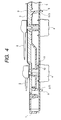
- Such an instrument has a structure shown in Fig. 4.
- a dial plate 3 in which a letter/scale portion is formed along an area where each of pointers 2 is swung is attached to a surface of a mounting part 1 such as a case.
- a circuit board 5 having circuit components such as movements 4 for swinging the pointers 2 is attached to the rear face of the mounting part 1 such as a case.
- Engaged portions 7 such as engagement holes 6 or engagement notches are formed in the circuit board 5.
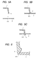
- Engagement claws 8 protrude from the mounting part 1. As shown in Figs. 5A to 5C, the engagement claws 8 are engaged with the engaged portions 7, respectively, to attach the circuit board 5 to the mounting part 1.
- the reference numeral 9 denotes a light guide plate which guides light emitted from a light source (not shown) to the letter/scale portions of the dial plate 3, base portions of the pointers 2, and the like.
- Reference numeral 10 denotes electrical connecting pins which elongate from the movements 4.
- Reference numeral 11 denotes solder for electrically connecting the electrical connecting pins 10 to the circuit board 5.
- the engaged portions 7 of the circuit board 5 are formed by a punching operation in press working, and hence edge portions have acute angles.
- the mounting part 1 such as a soft case, which is produced by, for example, injection-molding a PP composite material, is different in hardness from the hard circuit board 5, which is formed by stacking an epoxy resin, a paper phenol resin, and the like. Because of these reasons, when the engagement claws 8 are engaged with the engaged portions 7, a catch due to, for example, a bite between the edge portion of the engaged portion 7 and an inclined guide face, which is formed in a tip end of the engagement claws 8 occurs as shown in Fig. 6. This impairs the efficiency of the attaching work. There arises the possibility that, during the attaching work, this catch causes the harder circuit board 5 to crack or whittling to be produced.
- a structure for a circuit board attaching portion including a circuit board on which an engaged portion are formed and a mounting part in which an engaging claw are formed.
- the circuit board is attached to the mounting part by engaging the engaging claw with the engaged portion.
- a catch preventing portion which prevents the engaging claw from being caught, is formed on a side of a mounting part attached face of the engaged portion.
- the catch preventing portion is formed on a side of a mounting part attached face of the engaged portion. Even when an edge portion of the engaged portion has an acute angle or even when there is a difference in hardness between the circuit board and the mounting part, the catch preventing portion effectively prevents a catch between the engaged portion and the engagement claw from occurring. Therefore, the efficiency of the attaching work can be improved and the circuit board can be prevented from cracking.
- the catch preventing portion is an edge dulling portion, which is formed on an edge portion of the engaged portion.
- the edge dulling portion is formed as the catch preventing portion on the edge portion of the engaged portion, it is possible to prevent more effectively a catch between the engaged portion and the engagement claw from occurring.
- the edge dulling portion is a building up portion, which is formed on the edge portion of the engaged portion.
- the edge portion of the engaged portion can be dulled so that a catch between the engaged portion and the engagement claw can be prevented more effectively from occurring.
- the building up portion is solder.
- the edge portion of the engaged portion can be easily dulled so that a catch between the engaged portion and the engagement claw can be effectively prevented from occurring.
- the solder is disposed on a land, which is formed on the edge portion of the engaged portion.
- the solder since the solder is disposed on a land, which is formed on the edge portion of the engaged portion, the solder can be effectively disposed.
- the solder is formed concurrently with soldering of a circuit component onto the circuit board.
- the solder of the building up portion is formed concurrently with soldering of a circuit component onto the circuit board, it is not required to particularly form the catch preventing portion and hence the production cost can be suppressed.
- Figs. 1 to 3 show an embodiment of the invention. Parts identical or equivalent to those of the related art are denoted by the same reference numerals.
- An instrument having a speedometer, a tachometer, a fuel gauge, a water temperature gauge, and the like is attached in a vehicle such as an automobile.
- Such an instrument has a structure shown in Fig. 1.
- a dial plate 3 in which a letter/scale portion is formed along an area where each of pointers 2 is swung is attached to a surface of a mounting part 1 such as a case.
- a circuit board 5 having movements 4 for swinging the pointers 2 and electronic control circuit components are attached to the rear face of the mounting part 1 such as a case.
- Engaged portions 7 such as engagement holes 6 or engagement notches are formed in the circuit board 5.
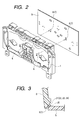
- Engagement claws 8 protrude from the mounting part 1. As shown in Fig. 2, the engagement claws 8 are engaged with the engaged portions 7, respectively, to attach the circuit board 5 to the mounting part 1.
- the reference numeral 9 denotes a light guide plate which guides light emitted from a light source (not shown) to the letter/scale portions, base portions of the pointers 2, and the like.
- Reference numeral 10 denotes electrical connecting pins, which elongate from the movements 4.
- Reference numeral 11 denotes solder for electrically connecting the electrical connecting pins 10 to the circuit board 5.
- a catch preventing portion 21 which prevents the engagement claw 8 from being caught is formed on a mounting part-attached face of each of the engaged portions 7.
- the catch preventing portion 21 is an edge dulling portion 22 which is formed on an edge portion of the engaged portion 7.
- the edge dulling portion 22 may be configured in various manners, and, for example, by chamfering the edge portion of the engaged portion 7.
- the unit is configured by forming a building up portion 23 on the edge portion of the engaged portion 7.
- the building up portion 23 may be configured in various manners, and, for example, by heaping an adhesive agent, a coating material, or a photoresist which is formed on the surface of the circuit board 5.
- the building up portion 23 is configured by solder 24.
- a land 25 is formed on the edge portion of the engaged portion 7, and the solder 24 is then disposed on the land 25.
- the solder 24 is formed concurrently with soldering of the circuit components onto the circuit board 5.
- the formation of the catch preventing portion 21 on the side of the mounting part-attached face of the engaged portion 7 prevents the inclined guide face of the engagement claw 8 from directly contacting with the acute edge of the engaged portions 7 and effectively prevents a catch between the engaged portion 7 and the engagement claw 8 from occurring. Therefore, the efficiency of the attaching work can be improved and the circuit board 5 can be prevented from cracking.
- edge dulling portion 22 is formed as the catch preventing portion 21 on the edge portion of the engaged portion 7, it is possible to prevent more effectively a catch between the engaged portion 7 and the engagement claw 8 from occurring.
- the building up portion 23 is formed as the edge dulling portion 22 on the edge portion of the engaged portion 7, the edge portion of the engaged portion 7 can be dulled. Therefore, a catch between the engaged portion 7 and the engagement claw 8 can be prevented more effectively from occurring.
- the edge portion of the engaged portion 7 can be easily dulled. Therefore, a catch between the engaged portion 7 and the engagement claw 8 can be prevented more effectively from occurring.
- solder 24 When the solder 24 is disposed on the land 25 which is formed on the edge portion of the engaged portion 7, the solder 24 can be effectively disposed.
- solder 24 of the building up portion 23 is formed concurrently with soldering of the circuit components onto the circuit board 5, it is not required to add a special process such as a process of chamfering the edge of the engaged portions 7. Therefore, the production cost can be suppressed.
- the engagement holes 6 or engagement notches are formed as the engaged portions 7. It is a matter of course that the outer peripheral edge of the circuit board 5 may be used as the engaged portions 7.
- the catch preventing portion is formed on the side of the mounting part attached face of the engaged portion. Even when the edge portion of the engaged portion has an acute angle or even when there is a difference in hardness between the circuit board and the mounting part, the catch preventing portion effectively prevents a catch between the engaged portion and the engagement claw from occurring. Therefore, the efficiency of the attaching work can be improved and the circuit board can be prevented from cracking.
- the edge dulling portion is formed as the catch preventing portion on the edge portion of the engaged portion, it is possible to prevent more effectively a catch between the engaged portion and the engagement claw from occurring.
- the edge portion of the engaged portion can be dulled so that a catch between the engaged portion and the engagement claw can be prevented more effectively from occurring.
- the edge portion of the engaged portion can be easily dulled so that a catch between the engaged portion and the engagement claw can be effectively prevented from occurring.
- the solder since the solder is disposed on a land, which is formed on the edge portion of the engaged portion, the solder can be effectively disposed.
- the solder of the building up portion is formed concurrently with soldering of a circuit component onto the circuit board, it is not required to particularly form the catch preventing portion. Therefore, it is possible to exert a practically useful effect that the production cost can be suppressed.
Landscapes
- Engineering & Computer Science (AREA)
- Manufacturing & Machinery (AREA)
- Microelectronics & Electronic Packaging (AREA)
- Mounting Of Printed Circuit Boards And The Like (AREA)
- Structure Of Printed Boards (AREA)
- Combinations Of Printed Boards (AREA)
- Electric Connection Of Electric Components To Printed Circuits (AREA)
Abstract
Description
Claims (7)
- A structure for a circuit board attaching portion comprising:a circuit board on which an engaged portion are formed; anda mounting part in which an engaging claw are formed,wherein the circuit board is attached to the mounting part by engaging the engaging claw with the engaged portion; andwherein a catch preventing portion, which prevents the engaging claw from being caught, is formed on a side of a mounting part attached face of the engaged portion.
- The structure according to claim 1, wherein the catch preventing portion is an edge dulling portion, which is formed on an edge portion of the engaged portion.
- The structure according to claim 2, wherein the edge dulling portion is a building up portion, which is formed on the edge portion of the engaged portion.
- The structure according to claim 3, wherein the building up portion is solder.
- The structure according to claim 4, wherein the solder is disposed on a land, which is formed on the edge portion of the engaged portion.
- The structure according to claim 4, wherein the solder is formed concurrently with soldering of a circuit component onto the circuit board.
- The structure according to claim 5, wherein the solder is formed concurrently with soldering of a circuit component onto the circuit board.
Applications Claiming Priority (2)
| Application Number | Priority Date | Filing Date | Title |
|---|---|---|---|
| JP2001296200A JP4050025B2 (en) | 2001-09-27 | 2001-09-27 | Circuit board mounting structure |
| JP2001296200 | 2001-09-27 |
Publications (3)
| Publication Number | Publication Date |
|---|---|
| EP1298971A2 true EP1298971A2 (en) | 2003-04-02 |
| EP1298971A3 EP1298971A3 (en) | 2005-02-02 |
| EP1298971B1 EP1298971B1 (en) | 2007-02-21 |
Family
ID=19117488
Family Applications (1)
| Application Number | Title | Priority Date | Filing Date |
|---|---|---|---|
| EP02021806A Expired - Lifetime EP1298971B1 (en) | 2001-09-27 | 2002-09-26 | Structure for circuit board mounting |
Country Status (4)
| Country | Link |
|---|---|
| US (1) | US6741481B2 (en) |
| EP (1) | EP1298971B1 (en) |
| JP (1) | JP4050025B2 (en) |
| DE (1) | DE60218258T2 (en) |
Families Citing this family (3)
| Publication number | Priority date | Publication date | Assignee | Title |
|---|---|---|---|---|
| JP2008070990A (en) * | 2006-09-12 | 2008-03-27 | Fujitsu Ltd | Electronic device and method of assembling the same |
| JP4365426B2 (en) * | 2007-04-13 | 2009-11-18 | カルソニックカンセイ株式会社 | Meter device |
| JP2011198954A (en) * | 2010-03-18 | 2011-10-06 | Denso Corp | Method for manufacturing circuit board mount |
Family Cites Families (10)
| Publication number | Priority date | Publication date | Assignee | Title |
|---|---|---|---|---|
| US3324226A (en) * | 1966-02-14 | 1967-06-06 | Ross Mfg Company | Component mountings |
| JPS6221585U (en) * | 1985-07-24 | 1987-02-09 | ||
| US5115375A (en) * | 1989-09-05 | 1992-05-19 | Switchcraft Inc. | Snap-in retainer sleeve |
| US5580203A (en) * | 1994-12-21 | 1996-12-03 | General Instrument Corporation Of Delaware | Resilient snap fitting retainer for printed circuit board mounting or the like |
| US6175509B1 (en) * | 1997-05-14 | 2001-01-16 | Hewlett-Packard Company | Space efficient local regulator for a microprocessor |
| US6431889B1 (en) * | 1997-12-23 | 2002-08-13 | Berg Technology, Inc. | High density edge card connector |
| US6095822A (en) * | 1998-01-13 | 2000-08-01 | Micron Technology, Inc. | Component module holder |
| US6260265B1 (en) * | 1998-04-27 | 2001-07-17 | Power Distribution Products | Circuit board stiffener |
| US6411522B1 (en) * | 1999-04-01 | 2002-06-25 | Western Digital Ventures, Inc. | Integrated computer module with EMI shielding plate |
| US6377475B1 (en) * | 2001-02-26 | 2002-04-23 | Gore Enterprise Holdings, Inc. | Removable electromagnetic interference shield |
-
2001
- 2001-09-27 JP JP2001296200A patent/JP4050025B2/en not_active Expired - Fee Related
-
2002
- 2002-09-26 US US10/254,847 patent/US6741481B2/en not_active Expired - Fee Related
- 2002-09-26 EP EP02021806A patent/EP1298971B1/en not_active Expired - Lifetime
- 2002-09-26 DE DE60218258T patent/DE60218258T2/en not_active Expired - Lifetime
Also Published As
| Publication number | Publication date |
|---|---|
| JP4050025B2 (en) | 2008-02-20 |
| EP1298971B1 (en) | 2007-02-21 |
| EP1298971A3 (en) | 2005-02-02 |
| JP2003101261A (en) | 2003-04-04 |
| DE60218258D1 (en) | 2007-04-05 |
| US6741481B2 (en) | 2004-05-25 |
| US20030072143A1 (en) | 2003-04-17 |
| DE60218258T2 (en) | 2007-06-14 |
Similar Documents
| Publication | Publication Date | Title |
|---|---|---|
| US6741481B2 (en) | Structure for circuit board attaching portion | |
| CN101448358B (en) | Flexible Printed Circuit Board Bending Area Structure | |
| US6163461A (en) | Terminal mounting structure for a printed circuit board | |
| TW373199B (en) | Method of manufacturing electronic components | |
| JP2003174281A (en) | Shield case for electronic components | |
| JP2008270304A (en) | Fixing structure of flexible flat cable to substrate | |
| JP2011070895A (en) | Board connector | |
| JPH1041594A (en) | Flexible printed circuit board | |
| JPH0747808Y2 (en) | Grounding member for metal plate | |
| JP4173050B2 (en) | Jack board positioning mechanism | |
| JP2000286524A (en) | Radial mounting component and substrate device using the same | |
| JPH08321693A (en) | Light emitting diode case arrangement structure and manufacturing method thereof | |
| JPH08203619A (en) | Mounting structure of coaxial connector and board | |
| JP2000012995A (en) | Device for attaching terminal parts to circuit board | |
| JPH06152076A (en) | Flexible circuit board | |
| JPH0432779Y2 (en) | ||
| JP2002368350A (en) | Printed circuit board structure | |
| JP2002329943A (en) | Component mounting board connection device | |
| JP2518641Y2 (en) | LCD mounting plate grounding structure | |
| JPS58102598A (en) | Automatic lead cutting device for printed board | |
| JPH10282475A (en) | Liquid crystal display | |
| US20030042594A1 (en) | Semiconductor package and method of manufacturing lead | |
| JPS5810889A (en) | How to divide a multi-cavity board | |
| JPS626711Y2 (en) | ||
| JP2002198632A (en) | Printed circuit board surface mount components and mounting method |
Legal Events
| Date | Code | Title | Description |
|---|---|---|---|
| PUAI | Public reference made under article 153(3) epc to a published international application that has entered the european phase |
Free format text: ORIGINAL CODE: 0009012 |
|
| AK | Designated contracting states |
Designated state(s): AT BE BG CH CY CZ DE DK EE ES FI FR GB GR IE IT LI LU MC NL PT SE SK TR Kind code of ref document: A2 Designated state(s): AT BE BG CH CY CZ DE DK EE ES FI FR GB GR IE IT LI LU MC NL PT SE SK TR |
|
| AX | Request for extension of the european patent |
Extension state: AL LT LV MK RO SI |
|
| PUAL | Search report despatched |
Free format text: ORIGINAL CODE: 0009013 |
|
| AK | Designated contracting states |
Kind code of ref document: A3 Designated state(s): AT BE BG CH CY CZ DE DK EE ES FI FR GB GR IE IT LI LU MC NL PT SE SK TR |
|
| AX | Request for extension of the european patent |
Extension state: AL LT LV MK RO SI |
|
| RIC1 | Information provided on ipc code assigned before grant |
Ipc: 7H 05K 3/30 A Ipc: 7H 05K 7/12 B Ipc: 7H 05K 7/14 B |
|
| 17P | Request for examination filed |
Effective date: 20050419 |
|
| 17Q | First examination report despatched |
Effective date: 20050519 |
|
| AKX | Designation fees paid |
Designated state(s): DE FR GB |
|
| GRAP | Despatch of communication of intention to grant a patent |
Free format text: ORIGINAL CODE: EPIDOSNIGR1 |
|
| GRAS | Grant fee paid |
Free format text: ORIGINAL CODE: EPIDOSNIGR3 |
|
| GRAA | (expected) grant |
Free format text: ORIGINAL CODE: 0009210 |
|
| AK | Designated contracting states |
Kind code of ref document: B1 Designated state(s): DE FR GB |
|
| REG | Reference to a national code |
Ref country code: GB Ref legal event code: FG4D |
|
| REF | Corresponds to: |
Ref document number: 60218258 Country of ref document: DE Date of ref document: 20070405 Kind code of ref document: P |
|
| ET | Fr: translation filed | ||
| PLBE | No opposition filed within time limit |
Free format text: ORIGINAL CODE: 0009261 |
|
| STAA | Information on the status of an ep patent application or granted ep patent |
Free format text: STATUS: NO OPPOSITION FILED WITHIN TIME LIMIT |
|
| 26N | No opposition filed |
Effective date: 20071122 |
|
| PGFP | Annual fee paid to national office [announced via postgrant information from national office to epo] |
Ref country code: GB Payment date: 20120926 Year of fee payment: 11 |
|
| PGFP | Annual fee paid to national office [announced via postgrant information from national office to epo] |
Ref country code: DE Payment date: 20120919 Year of fee payment: 11 Ref country code: FR Payment date: 20120926 Year of fee payment: 11 |
|
| GBPC | Gb: european patent ceased through non-payment of renewal fee |
Effective date: 20130926 |
|
| REG | Reference to a national code |
Ref country code: DE Ref legal event code: R119 Ref document number: 60218258 Country of ref document: DE Effective date: 20140401 |
|
| REG | Reference to a national code |
Ref country code: FR Ref legal event code: ST Effective date: 20140530 |
|
| PG25 | Lapsed in a contracting state [announced via postgrant information from national office to epo] |
Ref country code: GB Free format text: LAPSE BECAUSE OF NON-PAYMENT OF DUE FEES Effective date: 20130926 |
|
| PG25 | Lapsed in a contracting state [announced via postgrant information from national office to epo] |
Ref country code: DE Free format text: LAPSE BECAUSE OF NON-PAYMENT OF DUE FEES Effective date: 20140401 Ref country code: FR Free format text: LAPSE BECAUSE OF NON-PAYMENT OF DUE FEES Effective date: 20130930 |