EP1298591A2 - Lösung und Methodologie zur Erfassung von Oberflächenschäden auf einer kapazitiven Sensor mit integriertem Schaltung - Google Patents
Lösung und Methodologie zur Erfassung von Oberflächenschäden auf einer kapazitiven Sensor mit integriertem Schaltung Download PDFInfo
- Publication number
- EP1298591A2 EP1298591A2 EP02255633A EP02255633A EP1298591A2 EP 1298591 A2 EP1298591 A2 EP 1298591A2 EP 02255633 A EP02255633 A EP 02255633A EP 02255633 A EP02255633 A EP 02255633A EP 1298591 A2 EP1298591 A2 EP 1298591A2
- Authority
- EP
- European Patent Office
- Prior art keywords
- sensing surface
- electrolyte solution
- additional image
- image
- capacitive sensors
- Prior art date
- Legal status (The legal status is an assumption and is not a legal conclusion. Google has not performed a legal analysis and makes no representation as to the accuracy of the status listed.)
- Withdrawn
Links
Images


Classifications
-
- G—PHYSICS
- G01—MEASURING; TESTING
- G01N—INVESTIGATING OR ANALYSING MATERIALS BY DETERMINING THEIR CHEMICAL OR PHYSICAL PROPERTIES
- G01N21/00—Investigating or analysing materials by the use of optical means, i.e. using sub-millimetre waves, infrared, visible or ultraviolet light
- G01N21/84—Systems specially adapted for particular applications
- G01N21/88—Investigating the presence of flaws or contamination
- G01N21/95—Investigating the presence of flaws or contamination characterised by the material or shape of the object to be examined
- G01N21/956—Inspecting patterns on the surface of objects
- G01N21/95607—Inspecting patterns on the surface of objects using a comparative method
-
- G—PHYSICS
- G06—COMPUTING OR CALCULATING; COUNTING
- G06T—IMAGE DATA PROCESSING OR GENERATION, IN GENERAL
- G06T2207/00—Indexing scheme for image analysis or image enhancement
- G06T2207/30—Subject of image; Context of image processing
- G06T2207/30108—Industrial image inspection
- G06T2207/30148—Semiconductor; IC; Wafer
Definitions
- the present invention is directed, in general, to detecting defects in integrated circuits and, more specifically, to detecting surface damage or other irregularities at minute levels on the surface of capacitive sensor integrated circuits.
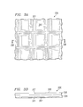
- FIGURE 3A is a plan view of a capacitive fingerprint sensor 300 showing the layout of capacitive sensor electrodes without overlying dielectric or passivation layers;
- FIGURE 3B is a cross-sectional view of the capacitive fingerprint sensor 300 taken at section line A-A, showing the overlying layers.
- Capacitive fingerprint sensor 300 includes a two dimensional array of pixels or cells each containing, in the example shown, a pair of capacitive sensor electrodes 301 and 302, formed by patterned conductive plates over a substrate containing devices (not shown) implementing the detection and control circuitry.
- An interlevel dielectric 304 e.g., an oxide
- a passivation layer 305 is disposed over the interlevel dielectric 304 and forms a sensor surface 306 on which the finger is placed for sensing of the fingerprint pattern.
- a problem with capacitive fingerprint sensors of the type described is localized surface damage 307 (e.g., scallops or troughs) and other irregularities in the sensing surface 306 of the top passivation layer 305.
- surface damage 307 e.g., scallops or troughs
- other irregularities in the sensing surface 306 of the top passivation layer 305 At the levels of 10 to 40 microns ( ⁇ m) in length and less than 1 ⁇ m wide, such surface irregularities are virtually impossible to detect with microscopic inspection. With such light damage, the fingerprint can still initially be detected by the affected pixels and the damage is not visible in the fingerprint image.
- the damage site degrades over time, modulating the pixel and changing the image.
- the pixel gain may degrade, for example, to approximately one third of the original gain, behaving as if coupled to a floating capacitive plate located in the region of the surface damage.
- the surface damage or irregularity thus manifests after roughly one to three months of use as a "white" region in the fingerprint image (i.e., a dead or largely insensitive region within the sensor array) resulting from an increase in the interference between coupling of the capacitor plates.
- Fingerprint sensor devices initially functioning properly therefore become functionally unacceptable after only a relatively brief period of use, without knowledge of--or any means for detecting--the surface damage or irregularity because no method of screening the problem was known.
- the electrolyte solution accelerates manifestation of pixel degradation and failure caused by surface damage or irregularities. Defective regions are identified by change of grayscale pixels in the preliminary image while the electrolyte coating is on the sensing surface and then again after the electrolyte coating is removed.
- FIGURES 1A-1B through 2A-2D discussed below, and the various embodiment used to describe the principles of the present invention in this patent document are by way of illustration only and should not be construed in any way to limit the scope of the invention. Those skilled in the art will understand that the principles of the present invention may be implemented in any suitably arranged device.
- FIGURES 1A and 1B depict detection of minute level surface damage or irregularity on the sensing surface of capacitive sensor integrated circuits according to one embodiment of the present invention.
- FIGURE 1A is a block diagram of a test system for detecting minute level surface damage on the sensing surface of capacitive integrated circuits.
- Test system 100 includes a testing unit 101 performing the process described below on testing subject 102.
- Testing subject 102 may be an individual capacitive integrated circuit, either before or after packaging, or a wafer containing a plurality of capacitive sensor integrated circuit die. In either case, however, testing unit 101 connects to the detection and control circuitry within the capacitive integrated circuit testing subject 102.
- FIGURE 1B is a high level flow chart for a process of detecting minute level surface damage or irregularity on the sensing surface of capacitive sensor integrated circuits according to one embodiment of the present invention.
- Process 103 begins with connection to the capacitive sensor array within the integrated circuit test subject 102 and initiation of testing (step 104).
- a preliminary image of the "grayscale" output of the capacitor sensor array i.e., the output before the sensitivity of the array is enhanced or degraded
- the sensing surface is then coated with an electrolyte solution to "decorate" the damaged regions or irregularities (step 106).
- a strong electrolyte solution such as sodium chloride (NaCl) is employed to accelerate changes to the capacitive array output which are normally seen only over time.
- the preferred electrolyte solution is one part saturated sodium chloride solution (in water) with two parts methanol.
- Other strong electrolytes such as potassium hydroxide (KaOH) solution or weak electrolytes such as citric acid or sodium bicarbonate solution may also be suitably employed.
- Silicon-based passivation materials used to form the sensing surface tend to be hydrophobic, such that a simple electrolyte solution will not wet the surface well. While alcohol solutions exhibit better surface tension, sodium chloride does not dissolve well in alcohol. Accordingly, the preferred electrolyte solution is a combination of saturated saline and methanol as described above, since the methanol breaks down the surface tension and promotes adhesion. However, other surfactants or solvents having low surface tension may be employed in lieu of alcohol or methanol, or may not be necessary depending on the composition of the sensing surface.
- the values of the capacitor readings are again taken (step 107) and compared with the original image.
- the presence of the electrolyte solution increases the capacitive coupling of the conductive plates forming the sensor array and the sensitivity of the pixels, acting as a grounded plate over the sensor array.
- any change to the functionality of the capacitive sensor array will appear with the affected pixels showing as black. In other image detection systems, however, the change may manifest in a different manner.
- the electrolyte solution is then be removed by a precision wipe (step 108), and the image is again taken by reading the pixel capacitance values (step 109). Pixels with surface damage or irregularities, which manifest as a localized floating plate or plates over the capacitive sensor conductive plates which collect charge, will now show in the image as white for an image detection system of the type described above. As noted, the change may manifest itself in a different manner when a different image detection mechanism is employed with the capacitive sensors.
- the images with the electrolyte solution present and after removal of the electrolyte solution are thus compared to the preliminary image (step 110), either visually or algorithmically, and the areas indicated to have surface damage or irregularities are identified by the change(s) in the pixels of the image. These locations may then be utilized with a scanning electron microscope (SEM) or optical microscope to locate the damage identified by decoration with the electrolyte solution.
- SEM scanning electron microscope
- Capacitive sensor integrated circuits which are found to have surface damage or irregularities may be either discarded or modified to disable the pixels affected by the surface damage if such modification permits acceptable performance. The process then becomes idle (step 111) until another capacitive sensor integrated circuit is tested.
- testing unit 101 includes a memory 112 for storing the image data during testing, as well as conventional processing modules (not shown) for comparing the image data and identifying changes and/or controlling the operation of testing unit 101.
- Testing system 100 may also include a data link 113 to the microscope 114 which is utilized to examine the sensing surface damage identified.
- FIGURES 2A through 2D illustrate capacitive sensor array images during detection of minute level surface damage or irregularities on the sensing surface according to one embodiment of the present invention. Each of the images was acquired with a single capacitive sensor integrated circuit.
- FIGURE 2A illustrates an initial "grayscale" image of a capacitive sensor array prior to application of an electrolyte solution. No surface damage or irregularities are visible.
- FIGURE 2B illustrates the image acquired by the same sensor array while the electrolyte solution is present on the sensing surface of the capacitive sensor integrated circuit.
- Narrow surface scratches 200 appear as lines within the image, with the lines appearing generally darker than undamaged pixels because of the pixel gain mechanism employed.
- FIGURE 2C illustrates the image of the sensor array after removal of the electrolyte solution, where at least some of the scratches remain apparent, but as white lines.
- FIGURE 2D illustrates a fingerprint image acquired utilizing the capacitor integrated circuit sensor after the damage was decorated out with the electrolyte solution. The scratches are clearly evident, superimposed on the fingerprint features.
- the present invention accelerates manifestation of the effect of extremely minute surface damage or irregularities on the sensing surface of a coupled-capacitance integrated circuit such as a fingerprint sensor.
- the damage or irregularities may be detected long prior to ordinary manifestation during use.
Landscapes
- Immunology (AREA)
- Pathology (AREA)
- Life Sciences & Earth Sciences (AREA)
- Chemical & Material Sciences (AREA)
- Analytical Chemistry (AREA)
- Biochemistry (AREA)
- General Health & Medical Sciences (AREA)
- General Physics & Mathematics (AREA)
- Health & Medical Sciences (AREA)
- Physics & Mathematics (AREA)
- Image Input (AREA)
- Measurement Of Length, Angles, Or The Like Using Electric Or Magnetic Means (AREA)
- Image Processing (AREA)
- Image Analysis (AREA)
- Investigating Materials By The Use Of Optical Means Adapted For Particular Applications (AREA)
- Measurement Of The Respiration, Hearing Ability, Form, And Blood Characteristics Of Living Organisms (AREA)
- Testing Or Measuring Of Semiconductors Or The Like (AREA)
Applications Claiming Priority (2)
| Application Number | Priority Date | Filing Date | Title |
|---|---|---|---|
| US943597 | 2001-08-30 | ||
| US09/943,597 US6545486B2 (en) | 2001-08-30 | 2001-08-30 | Solution and methodology for detecting surface damage on capacitive sensor integrated circuit |
Publications (2)
| Publication Number | Publication Date |
|---|---|
| EP1298591A2 true EP1298591A2 (de) | 2003-04-02 |
| EP1298591A3 EP1298591A3 (de) | 2006-04-19 |
Family
ID=25479916
Family Applications (1)
| Application Number | Title | Priority Date | Filing Date |
|---|---|---|---|
| EP02255633A Withdrawn EP1298591A3 (de) | 2001-08-30 | 2002-08-13 | Lösung und Methodologie zur Erfassung von Oberflächenschäden auf einer kapazitiven Sensor mit integriertem Schaltung |
Country Status (3)
| Country | Link |
|---|---|
| US (1) | US6545486B2 (de) |
| EP (1) | EP1298591A3 (de) |
| JP (1) | JP4243750B2 (de) |
Cited By (2)
| Publication number | Priority date | Publication date | Assignee | Title |
|---|---|---|---|---|
| EP3188078A1 (de) * | 2015-12-29 | 2017-07-05 | Xiaomi Inc. | Verfahren und vorrichtung zur fingerabdruckidentifizierung |
| CN107742111A (zh) * | 2017-11-03 | 2018-02-27 | 北京小米移动软件有限公司 | 身份识别方法及装置、存储介质 |
Families Citing this family (7)
| Publication number | Priority date | Publication date | Assignee | Title |
|---|---|---|---|---|
| US8692777B2 (en) * | 2008-02-08 | 2014-04-08 | Apple Inc. | Method for rapidly testing capacitance sensing array fault conditions using a floating conductor |
| SE1550411A1 (en) | 2015-04-07 | 2016-10-08 | Fingerprint Cards Ab | Electronic device comprising fingerprint sensor |
| CN105224931B (zh) * | 2015-10-19 | 2018-05-08 | 广东欧珀移动通信有限公司 | 一种指纹采集方法及装置 |
| CN107644220B (zh) * | 2017-09-30 | 2021-03-05 | 上海摩软通讯技术有限公司 | 移动终端的指纹识别方法及系统 |
| CN108197550A (zh) * | 2017-12-28 | 2018-06-22 | 北京小米移动软件有限公司 | 故障提示方法、装置及电子设备 |
| CN114829955A (zh) * | 2020-11-05 | 2022-07-29 | 指纹卡安娜卡敦知识产权有限公司 | 用于指纹传感器评估的方法和系统 |
| CN121190558B (zh) * | 2025-10-14 | 2026-04-07 | 东莞市宏诚光学制品有限公司 | 一种光学镜片镀膜缺陷检测方法及系统 |
Family Cites Families (6)
| Publication number | Priority date | Publication date | Assignee | Title |
|---|---|---|---|---|
| SU756282A1 (ru) * | 1978-06-30 | 1980-08-15 | Georgij N Pavlov | Электролит для определения дефектов диэлектрических пленок |
| KR960007481B1 (ko) * | 1991-05-27 | 1996-06-03 | 가부시끼가이샤 히다찌세이사꾸쇼 | 패턴검사방법 및 장치 |
| IL102659A (en) * | 1992-07-27 | 1997-07-13 | Orbot Instr Ltd | Apparatus and method for comparing and aligning two digital representations of an image |
| US5907627A (en) * | 1995-11-06 | 1999-05-25 | Dew Engineering And Development Limited | Contact imaging device |
| US6114862A (en) * | 1996-02-14 | 2000-09-05 | Stmicroelectronics, Inc. | Capacitive distance sensor |
| WO1999010714A1 (en) * | 1997-08-25 | 1999-03-04 | Millennium Sensors Ltd. | A compensated capacitive liquid level sensor |
-
2001
- 2001-08-30 US US09/943,597 patent/US6545486B2/en not_active Expired - Lifetime
-
2002
- 2002-08-13 EP EP02255633A patent/EP1298591A3/de not_active Withdrawn
- 2002-08-30 JP JP2002252419A patent/JP4243750B2/ja not_active Expired - Fee Related
Cited By (6)
| Publication number | Priority date | Publication date | Assignee | Title |
|---|---|---|---|---|
| EP3188078A1 (de) * | 2015-12-29 | 2017-07-05 | Xiaomi Inc. | Verfahren und vorrichtung zur fingerabdruckidentifizierung |
| CN106934320A (zh) * | 2015-12-29 | 2017-07-07 | 小米科技有限责任公司 | 指纹识别方法及装置 |
| US10216976B2 (en) | 2015-12-29 | 2019-02-26 | Xiaomi Inc. | Method, device and medium for fingerprint identification |
| CN106934320B (zh) * | 2015-12-29 | 2020-03-17 | 小米科技有限责任公司 | 指纹识别方法及装置 |
| CN107742111A (zh) * | 2017-11-03 | 2018-02-27 | 北京小米移动软件有限公司 | 身份识别方法及装置、存储介质 |
| CN107742111B (zh) * | 2017-11-03 | 2021-11-02 | 北京小米移动软件有限公司 | 身份识别方法及装置、存储介质 |
Also Published As
| Publication number | Publication date |
|---|---|
| US20030042911A1 (en) | 2003-03-06 |
| JP4243750B2 (ja) | 2009-03-25 |
| EP1298591A3 (de) | 2006-04-19 |
| US6545486B2 (en) | 2003-04-08 |
| JP2003123054A (ja) | 2003-04-25 |
Similar Documents
| Publication | Publication Date | Title |
|---|---|---|
| US7315642B2 (en) | System and method for measuring thin film thickness variations and for compensating for the variations | |
| JP4351522B2 (ja) | パターン欠陥検査装置およびパターン欠陥検査方法 | |
| US7894659B2 (en) | Methods for accurate identification of an edge of a care area for an array area formed on a wafer and methods for binning defects detected in an array area formed on a wafer | |
| US8126259B2 (en) | Method and apparatus for visual inspection | |
| US5640237A (en) | Method and apparatus for detecting non-uniformities in reflective surafaces | |
| US20040057611A1 (en) | Method for selecting reference images, method and apparatus for inspecting patterns on wafers, and method for dividing a wafer into application regions | |
| CN111426701B (zh) | 一种晶圆缺陷检测方法及其装置 | |
| WO2010093733A2 (en) | Detecting defects on a wafer | |
| US6545486B2 (en) | Solution and methodology for detecting surface damage on capacitive sensor integrated circuit | |
| KR100335491B1 (ko) | 공정 파라미터 라이브러리를 내장한 웨이퍼 검사장비 및 웨이퍼 검사시의 공정 파라미터 설정방법 | |
| CN114402192B (zh) | 用于晶片缺陷检测的基于变化的分段 | |
| US6909798B1 (en) | Method of erasing repeated patterns and pattern defect inspection device | |
| US8094926B2 (en) | Ultrafine pattern discrimination using transmitted/reflected workpiece images for use in lithography inspection system | |
| US7046352B1 (en) | Surface inspection system and method using summed light analysis of an inspection surface | |
| JP6259634B2 (ja) | 検査装置 | |
| JP2006300892A (ja) | カラーフィルタ形成基板の異物検査方法およびカラーフィルタ形成基板の異物検査装置 | |
| CN111855663B (zh) | 一种检测晶圆缺陷的设备和方法 | |
| KR100516828B1 (ko) | 광학적 검사의 과검출 방지 방법 및 이를 수행하기 위한 시스템 | |
| JP2004361329A (ja) | パターン検査方法および装置 | |
| JPH0617875B2 (ja) | パターン検査方法およびその装置 | |
| KR100268778B1 (ko) | 반도체소자의 공정결함 검사방법 | |
| TW202601551A (zh) | 用於半導體裝置檢測的深度影像產生方法及深度影像產生系統 | |
| KR20030023336A (ko) | 반도체장치의 결함 검출방법 | |
| Nozoe et al. | Recent technology for particle detection on patterned wafers | |
| KR20000027842A (ko) | 반도체장치의 결함검사방법 |
Legal Events
| Date | Code | Title | Description |
|---|---|---|---|
| PUAI | Public reference made under article 153(3) epc to a published international application that has entered the european phase |
Free format text: ORIGINAL CODE: 0009012 |
|
| AK | Designated contracting states |
Kind code of ref document: A2 Designated state(s): AT BE BG CH CY CZ DE DK EE ES FI FR GB GR IE IT LI LU MC NL PT SE SK TR Designated state(s): AT BE BG CH CY CZ DE DK EE ES FI FR GB GR IE IT LI LU MC NL PT SE SK TR |
|
| AX | Request for extension of the european patent |
Extension state: AL LT LV MK RO SI |
|
| RAP1 | Party data changed (applicant data changed or rights of an application transferred) |
Owner name: UPEK INC., |
|
| PUAL | Search report despatched |
Free format text: ORIGINAL CODE: 0009013 |
|
| AK | Designated contracting states |
Kind code of ref document: A3 Designated state(s): AT BE BG CH CY CZ DE DK EE ES FI FR GB GR IE IT LI LU MC NL PT SE SK TR |
|
| AX | Request for extension of the european patent |
Extension state: AL LT LV MK RO SI |
|
| RIC1 | Information provided on ipc code assigned before grant |
Ipc: G06K 9/00 20060101ALI20060228BHEP Ipc: G01N 21/88 20060101ALI20060228BHEP Ipc: G06T 7/00 20060101AFI20030204BHEP |
|
| AKX | Designation fees paid | ||
| REG | Reference to a national code |
Ref country code: DE Ref legal event code: 8566 |
|
| STAA | Information on the status of an ep patent application or granted ep patent |
Free format text: STATUS: THE APPLICATION IS DEEMED TO BE WITHDRAWN |
|
| 18D | Application deemed to be withdrawn |
Effective date: 20061020 |