EP1296379A2 - Schottky barrier diode and method for manufacturing it - Google Patents
Schottky barrier diode and method for manufacturing it Download PDFInfo
- Publication number
- EP1296379A2 EP1296379A2 EP02017076A EP02017076A EP1296379A2 EP 1296379 A2 EP1296379 A2 EP 1296379A2 EP 02017076 A EP02017076 A EP 02017076A EP 02017076 A EP02017076 A EP 02017076A EP 1296379 A2 EP1296379 A2 EP 1296379A2
- Authority
- EP
- European Patent Office
- Prior art keywords
- layer
- barrier diode
- schottky barrier
- substrate
- bonding pad
- Prior art date
- Legal status (The legal status is an assumption and is not a legal conclusion. Google has not performed a legal analysis and makes no representation as to the accuracy of the status listed.)
- Withdrawn
Links
Images



Classifications
-
- H—ELECTRICITY
- H10—SEMICONDUCTOR DEVICES; ELECTRIC SOLID-STATE DEVICES NOT OTHERWISE PROVIDED FOR
- H10D—INORGANIC ELECTRIC SEMICONDUCTOR DEVICES
- H10D8/00—Diodes
- H10D8/01—Manufacture or treatment
- H10D8/051—Manufacture or treatment of Schottky diodes
-
- H—ELECTRICITY
- H10—SEMICONDUCTOR DEVICES; ELECTRIC SOLID-STATE DEVICES NOT OTHERWISE PROVIDED FOR
- H10D—INORGANIC ELECTRIC SEMICONDUCTOR DEVICES
- H10D8/00—Diodes
- H10D8/60—Schottky-barrier diodes
-
- H—ELECTRICITY
- H10—SEMICONDUCTOR DEVICES; ELECTRIC SOLID-STATE DEVICES NOT OTHERWISE PROVIDED FOR
- H10W—GENERIC PACKAGES, INTERCONNECTIONS, CONNECTORS OR OTHER CONSTRUCTIONAL DETAILS OF DEVICES COVERED BY CLASS H10
- H10W72/00—Interconnections or connectors in packages
- H10W72/90—Bond pads, in general
-
- H—ELECTRICITY
- H10—SEMICONDUCTOR DEVICES; ELECTRIC SOLID-STATE DEVICES NOT OTHERWISE PROVIDED FOR
- H10W—GENERIC PACKAGES, INTERCONNECTIONS, CONNECTORS OR OTHER CONSTRUCTIONAL DETAILS OF DEVICES COVERED BY CLASS H10
- H10W70/00—Package substrates; Interposers; Redistribution layers [RDL]
- H10W70/60—Insulating or insulated package substrates; Interposers; Redistribution layers
-
- H—ELECTRICITY
- H10—SEMICONDUCTOR DEVICES; ELECTRIC SOLID-STATE DEVICES NOT OTHERWISE PROVIDED FOR
- H10W—GENERIC PACKAGES, INTERCONNECTIONS, CONNECTORS OR OTHER CONSTRUCTIONAL DETAILS OF DEVICES COVERED BY CLASS H10
- H10W72/00—Interconnections or connectors in packages
- H10W72/50—Bond wires
- H10W72/531—Shapes of wire connectors
- H10W72/5363—Shapes of wire connectors the connected ends being wedge-shaped
-
- H—ELECTRICITY
- H10—SEMICONDUCTOR DEVICES; ELECTRIC SOLID-STATE DEVICES NOT OTHERWISE PROVIDED FOR
- H10W—GENERIC PACKAGES, INTERCONNECTIONS, CONNECTORS OR OTHER CONSTRUCTIONAL DETAILS OF DEVICES COVERED BY CLASS H10
- H10W72/00—Interconnections or connectors in packages
- H10W72/50—Bond wires
- H10W72/551—Materials of bond wires
- H10W72/552—Materials of bond wires comprising metals or metalloids, e.g. silver
- H10W72/5522—Materials of bond wires comprising metals or metalloids, e.g. silver comprising gold [Au]
-
- H—ELECTRICITY
- H10—SEMICONDUCTOR DEVICES; ELECTRIC SOLID-STATE DEVICES NOT OTHERWISE PROVIDED FOR
- H10W—GENERIC PACKAGES, INTERCONNECTIONS, CONNECTORS OR OTHER CONSTRUCTIONAL DETAILS OF DEVICES COVERED BY CLASS H10
- H10W72/00—Interconnections or connectors in packages
- H10W72/50—Bond wires
- H10W72/59—Bond pads specially adapted therefor
Definitions
- the invention relates to a Schottky barrier diode device made of a compound semiconductor and applied in a high frequency circuit, specifically to a Schottky barrier diode having a planar configuration to achieve a smaller operation region and a smaller overall chip size, and to a manufacturing method of such a Schottky barrier diode.
- FET field effect transistors
- GaAs gallium arsenide
- Typical application in this field includes local oscillation FETs for satellite antenna and monolithic microwave integrated circuits (MMIC) in which a plurality of FETs are integrated for wireless broadband.
- MMIC monolithic microwave integrated circuits
- GaAs Schottky barrier diodes are also used in a base station of cellular phone system.
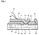
- FIG. 1 is a cross-sectional view including an operation region of a conventional Schottky barrier diode.
- An n+ epitaxial layer 22 (a silicon impurity concentration of about 5x10 18 cm -3 ) having a thickness of about 6 ⁇ m is formed on an n+ GaAs substrate 21.
- An n epitaxial layer 23 (a silicon impurity concentration of about 1.3x10 17 cm -3 ) having a thickness of about 350 nm is formed on the n+ epitaxial layer 22. This n epitaxial layer provides as an operation region.
- An ohmic electrode 28 makes a ohmic contact with the n+ epitaxial layer 22 and is made of a AuGe (gold-germanium alloy)/Ni (nickel) /Au (gold) metal layer disposed as a first wiring layer.
- a Ti (titanium)/Pt (platinum)/Au metal 32 serves as a second wiring layer, and is divided into wiring on the anode side and wiring on the cathode side.
- the Ti/Pt/Au metal layer makes a Schottky contact with the n epitaxial layer 23, and forms a Schottky contact region 31a.
- the portion of the Ti/Pt/Au metal layer on the anode side above the Schottky contact region 31a is referred to as a Schottky electrode 31.
- An anode electrode 34 is formed on and completely overlaps with the Schottky electrode 31 and its extension.
- the anode electrode 34 provides an anode bonding pad 34a and is formed by Au plating using the Schottky electrode 31 and its extension as a plating electrode.
- a bonding wire 40 is fixed to the anode bonding pad 34a.
- the Au metal layer serves as a third wiring layer and has a thickness of about 6 ⁇ m. The thick Au layer is necessary for providing stress relief during wire bonding.
- the cathode electrode 35 provides a cathode bonding pad and is formed of the Au layer.
- the Ti/Pt/Au metal layer on the cathode side directly contacts the ohmic electrode 28.
- the edge of the Schottky electrode 31 needs to be on a top surface of a polyimide layer 30 to satisfy photolithographic requirements. Accordingly, a portion of the Schottky electrode 31, near the Schottky region 31a, overlaps by about 16 ⁇ m with the polyimide layer 30 formed on the ohmic electrode 28 on the cathode side.
- the entire substrate and epitaxial layers are at a cathode voltage except the Schottky contact region 31a.
- the polyimide layer 30 insulates the anode electrode 34 from the substrate 22 and the epitaxial layers.
- the intersection between the anode electrode 34 and the underlying structure and the intersection between the anode bonding pad 34a and the underlying structure are, in total, about 3900 ⁇ m 2 , which could provide a large parasitic capacitance to the device if the thickness of the polyimide layer 30 is small.
- the thickness of the polyimide layer must be as large as 6-7 ⁇ m even though the polyimide film 30 has a relatively low dielectric constant.
- the n epitaxial layer 23 of the lower impurity concentration (1.3x10 17 cm -3 ) is necessary for assuring a Schottky contact region 31a with good Schottky characteristics and a high breakdown strength (10V).
- the ohmic electrode 28 is formed directly on the n+ epitaxial layer 22 for reducing the resistance at the contact. For this reason, a mesa etching process is necessary for exposing the top surface of the n+ epitaxial layer 22.
- the n+ GaAs substrate 21 underneath the n+ epitaxial layer 22 also has a high impurity concentration, and has a backside electrode made of the AuGe/Ni/Au metal layer for an external contact from the backside.
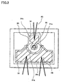
- FIG. 2 is a schematic top view of the conventional Schottky barrier diode having the operation region shown in FIG. 1.
- the Schottky contact region 31a formed in the n epitaxial layer 23 occupies a central portion of the device.
- the diameter of this region 31a is about 10 ⁇ m.
- a Schottky contact hole 29 is formed in the center of the Schottky contact region 31a.
- the Ti/Pt/Au metal layer of the second wiring layer is in direct contact with the n epitaxial layer 23 through the contact hole 29.
- the ohmic electrode 28 of the first wiring layer surrounds the circular Schottky contact region 31a, and occupies almost a half of the top surface of the device.
- the Au metal layer of the third wiring layer provides the bonding pads.
- the anode bonding pad 34a has a minimum area allowed for one bonding wire 40.
- the cathode bonding pad 35a is large enough to provide bonding of multiple wires 40, which is required for reducing the inductance generated at bonding wires.
- the cathode bonding pad 35a and the cathode electrode 35 are formed directly on the ohmic electrode 8 disposed on the n+ epitaxial layer without the intervening polyimide layer 30.
- the area of the anode bonding pad 34a is about 40 x 60 ⁇ m 2 and the area for the cathode bonding pad is about 240 x 70 ⁇ m 2 .
- the mesa etching which is required to expose the n+ epitaxial layer 22 through the n epitaxial layer 23 for the direct contact with the ohmic electrode 28, is not stable enough to provide accurate patterning of the device.
- the wet etching process used in the mesa etching may remove the oxide film 25 around the contact hole 29, leading to formation of mesa with an irregular shape.
- Such an irregular mesa structure may cause adverse effects on the Schottky barrier diode, especially the characteristics of the Schottky contact region 31a.
- the polyimide layer 30 has a thickness as large as 6-7 ⁇ m to reduce the parasitic capacitance generated between the Schottky electrode 31 and the underlying structures (the epitaxial layers 22, 23 and the substrate 21) at the cathode voltage.
- the edges of the polyimide layer 30 near the Schottky contact region 31a must have a tapered cross-section, as shown in FIG. 1.
- Such a tapered structure gives rise to a variation of the tapering angle, typically between 30 and 45 degrees.
- a long separation between the Schottky contact region 31a and the ohmic electrode 28 is required. This separation leads to a large resistance and, thus, poor high frequency characteristics.
- the device shown in FIG. 1 has a separation of about 7 ⁇ m.
- the large area (2400 ⁇ m 2 ) of the anode bonding pad 34a further contributes to the increase of the parasitic capacitance of the diode device.
- the polyimide layer 30 and the thick Au layer are made of expensive materials and their use inevitably increases the production cost.
- the objection of this invention is to provide a Schottky barrier method and manufacturing method of a Schottky barrier diode that lessen these drawbacks.
- the invention provides a Schottky barrier diode including a substrate made of a compound semiconductor and an epitaxially grown layer disposed on the substrate.
- the Schottky contact region of the device is a part of the epitaxially grown layer.
- An anode wiring is connected to the Schottky contact region.
- An insulating region penetrates through the epitaxially grown layer and reaches the substrate.
- An anode bonding pad is disposed on the insulating region and connected the anode wiring.
- the invention also provides a Schottky barrier diode including a substrate made of a compound semiconductor and an epitaxially grown layer disposed on the substrate.
- the Schottky contact region of the device is a part of the epitaxially grown layer.
- An anode wiring is connected to the Schottky contact region.
- An insulating region penetrates through the epitaxially grown layer and reaches the substrate.
- An anode bonding pad is disposed on the epitaxially grown layer and connected to the anode wiring. The insulating region surrounds the anode bonding pad.
- the invention further provides a Schottky barrier diode including a substrate made of a compound semiconductor and an epitaxially grown layer of a conduction type disposed on the substrate, which includes a Schottky contact region.
- An anode wiring is connected to the Schottky contact region.
- An insulating region penetrates through the epitaxially grown layer and reaches the substrate.
- a first impurity-implanted region of the conduction type penetrates through the epitaxially grown layer.
- An anode bonding pad is disposed on the first impurity-implanted region and connected to the anode wiring. The insulating region surrounds the anode bonding pad.
- the invention further provides a Schottky barrier diode including a substrate made of a compound semiconductor and an epitaxially grown layer of a conduction type disposed on the substrate, which includes a Schottky contact region.
- An anode wiring is connected to the Schottky contact region.
- An anode bonding pad is disposed on the epitaxially grown layer and connected to the anode wiring.
- a first impurity-implanted region of the conduction type penetrates through the epitaxially grown layer and is disposed underneath a peripheral portion of the anode bonding pad.
- An insulating region penetrates through the epitaxially grown layer to reach the substrate and surrounds the first impurity-implanted region.
- the invention provides a manufacturing method of Schottky barrier diode including providing a substrate made of a compound semiconductor and epitaxially growing a first layer of a conduction type on the substrate. An insulating region is formed at a predetermined portion of the first layer so that the insulating region reaches the substrate. A metal layer is formed to make a Schottky contact with the first layer and to provide an anode bonding pad.
- the invention also provides a manufacturing method of Schottky barrier diode including providing a substrate made of a compound semiconductor and epitaxially growing a first layer of a conduction type on the substrate. An impurity-implanted region of the conduction type is formed at a predetermined portion of the first layer. An insulating region is formed around the impurity-implanted region so that the insulating region reaches the substrate. A metal layer is formed to make a Schottky contact with the first layer and to provide an anode bonding pad.
- FIG. 1 is a cross-sectional view of a conventional Schottky barrier diode having a polyimide layer.
- FIG. 2 is a schematic top view of the conventional device of FIG. 1.
- FIG. 3 is a cross-sectional view of a Schottky barrier diode of a first embodiment of this invention.
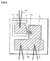
- FIG. 4 is a schematic top view of the device of the first embodiment.
- FIG. 5 is a first modification of the device of the first embodiment.
- FIG. 6 is a second modification of the device of the first embodiment.
- FIGS. 7A-7E show processing steps of a manufacturing method of the Schottky barrier diode of the first embodiment.
- FIG. 8 is a cross-sectional view of a Schottky barrier diode of a second embodiment of this invention.
- FIG. 9 is a schematic top view of the device of the second embodiment.
- FIG. 10 is a first modification of the device of the second embodiment.
- FIGS. 11A-11E show processing steps of a manufacturing method of the Schottky barrier diode of the second embodiment.
- FIG. 3 is a cross-sectional view of a Schottky barrier diode of a first embodiment of this invention. Specifically, FIG. 3 focuses on an operation region of the first embodiment.
- the compound semiconductor substrate 1 of this embodiment is an undoped GaAs substrate.
- An n+ epitaxial layer 2 having a thickness of about 500 nm and a silicon impurity concentration of about 5 x 10 18 cm -3 is formed on the substrate 1.
- An n epitaxial layer 3 having a thickness of about 250 nm and a silicon impurity concentration of about 1.3 x 10 17 cm -3 is formed on the n+ epitaxial layer 2.
- the n+ epitaxial layer 2 is much thinner than the n+ epitaxial layer 22 of the conventional device of FIG. 1 so that an insulating region 6 easily reaches the substrate 1 in an impurity injection process as described later.
- the device of the first embodiment has a planar configuration without any mesa structure.
- An impurity-implanted region 7 is formed underneath the ohmic electrode 8, and penetrates through the n epitaxial layer 3 to reach the n+ epitaxial layer 2.
- the impurity-implanted region 7 surrounds a circular Schottky contact region 11a, which is a part of the n epitaxial layer 3, and completely overlaps with an ohmic electrode 8.
- the impurity-implanted region 7 slightly extends beyond the ohmic electrode 8 and toward the Schottky contact region 11a.
- the separation between the Schottky contact region 11a and the impurity-implanted region 7 is 1 ⁇ m.
- the impurity-implanted region 7, which reaches from the ohmic electrode 8 to the n+ epitaxial layer 2 through the n epitaxial layer 3, replaces the mesa structure of conventional device and, thus achieves a planar device structure.
- a nitride film 5 insulates an anode electrode 11 from the ohmic electrode 8, the n+ epitaxial layer 2 and the n epitaxial layer 3, which are at a cathode voltage.
- the ohmic electrode 8 disposed on the impurity-implanted region 7 is a part of a first wiring layer made of a AuGe/Ni/Au metal layer.
- the first wiring layer is formed by depositing AuGe, Ni and Au films in this order.
- the ohmic electrode 8 has a rectangular shape with a hole corresponding to the Schottky contact region 11a (FIG. 4). The separation between the Schottky contact region 11a and the ohmic electrode 8 is about 2 ⁇ m.
- the portion of the anode electrode 11 above the Schottky contact region 11a makes a Schottky contact with the n epitaxial layer 3 through a Schottky contact hole formed in the nitride film 5 covering the surface of the n epitaxial layer 3.
- the Schottky contact region 11a has a diameter of about 10 ⁇ m, and provides an operation region of the Schottky barrier diode.
- the thickness of the n epitaxial layer 3 (250 nm) is determined to assure a proper breakdown voltage.
- An insulating region 6 is formed underneath an anode bonding pad 11b by implanting boron ions into the epitaxial layers 2, 3 and the substrate 1.
- the insulating region 6 should at least reach the insulating substrate 1.
- the cathode electrode 15 is formed of a second wiring layer made of a Ti/Pt/Au metal layer and is in contact with the ohmic electrode 8. One end of the cathode electrode 15 faces the anode electrode 11, and other end extends to a cathode bonding pad 15b, which is formed as a part of the second wiring layer. In other words, the cathode electrode 15 provides wiring between the ohmic electrode 8 and the cathode bonding pad 15a.
- the cathode bonding pad 15a is disposed directly on the n epitaxial layer 3. Accordingly, the impurity-implanted region 7, which is in contact with the ohmic electrode 8, and the n+ epitaxial layer 2 are at the cathode voltage.
- the anode electrode 11 is formed of the second wiring layer made of a Ti/Pt/Au metal layer and provides wiring between the Schottky contact region 11a and the anode bonding pad 11b. One end of the anode electrode 11 is in contact with the Schottky contact region 11a, and other end extends to the anode bonding pad 11b, which is formed as a part of the second wiring layer.
- the cathode electrode 15 provides wiring between the ohmic electrode 8 and the cathode bonding pad 15a.
- the cathode bonding pad 15a is disposed directly on the n epitaxial layer 3.
- the anode bonding pad 11b is insulated from the n epitaxial layer 3 and the n+ epitaxial layer 2, which are at the cathode voltage, by the insulating region 6. Accordingly, high frequency signal leakage at the anode bonding pad 11b can be prevented. Furthermore, because there is no structure contributing to capacitance formation underneath the anode bonding pad 11b, the overall parasitic capacitance of the Schottky barrier diode of this embodiment is reduced.
- Two bonding wires 40 are fixed to the anode bonding pad 11b.
- Four bonding wires 40 are fixed to the cathode bonding pad 15b.
- a stitch bonding process is applied to the fixation of the bonding wires 40 to the corresponding bonding pads 11b, 15b because the stitch bonding can fix two wires on the bonding pad in one bonding procedure, and, thus, reduce the required area for the bonding.
- FIG. 4 is a schematic top view of the Schottky barrier diode of the first embodiment.
- the Schottky contact region 11a is located approximately in the center of the GaAs chip.
- the insulating region 6 is larger than the anode bonding pad 11b, which is formed on the insulating region 6.
- the area denoted by the broken line is the ohmic electrode 8.
- the impurity-implanted region 7 (omitted form FIG. 4) is formed underneath the ohmic electrode 8 and covers approximately the same area of the substrate as the ohmic electrode 8.
- the Schottky contact region 11a is located in the hole created in the ohmic electrode 8.
- the cathode electrode 15 made of the second wiring layer is disposed on the ohmic electrode 8 to serve as wiring leading to the cathode bonding pad 15a.
- the external connection of the cathode electrode 15 has a significant influence on the high frequency characteristics, including inductance, of the Schottky barrier diode.
- the size of the cathode bonding pad 15a is large enough to provide multiple wire for reducing the inductance.
- the area of the anode bonding pad 11b is about 60 x 70 ⁇ m, and the area of the cathode bonding pad 15a is about 180 x 70 ⁇ m.
- intersection between the anode electrode 11 and the n epitaxial layer 3, which is at the cathode voltage, is about 100 ⁇ m 2 , which is about one thirty ninth of the intersection area of conventional device (3900 ⁇ m 2 ). Because of this reduction, the polyimide layer of conventional device can be replaced by a much thinner nitride film 5.
- the separation between the Schottky contact region 11a and the ohmic electrode 8 is reduced to about 2 ⁇ m, and the separation between the Schottky contact region 11a and the impurity-implanted region 7 is reduced to about 1 ⁇ m, in comparison to the conventional device, which has a separation of about 7 ⁇ m.
- the impurity-implanted region is similar to the ohmic electrode 8 in terms of carrier conduction, the device of this embodiment has a separation of about one seventh of the conventional device. This leads to an improvement of high frequency characteristics over the conventional device since a shorter separation provides a smaller resistance.
- the chip size reduces from 0.27 x 0.31 mm 2 of the conventional device to 0.25 x 0.25 mm 2 of this embodiment.
- the size of the operation region, or the Schottky contact region 11a is smaller than that of the conventional device by about one tenth.
- the insulating region 6 is not completely electrically insulating. Thus, it may be possible that a depletion layer is formed underneath the anode bonding pad 11b, which is made of the second wiring layer, and that the depletion layer reaches the ohmic electrode 8 depending on the high frequency signals the anode bonding pad 11b receives. If this happens, significant high frequency signal leakage results. However, in this embodiment, the depletion layer is prevented from reaching the ohmic electrode 8 by the impurity-implanted region 7 and n+ epitaxial layer 2, both of which are capable of absorbing the depletion layer. Accordingly, the anode-cathode interference is eliminated and the two electrodes are completely separated in terms of high frequency signals.
- the anode electrode 11 is formed by evaporating a Ti film, a Pt film and a Au film in this order.
- a thin anode electrode 11 is applicable in this embodiment because the thick polyimide layer of the conventional diode device is replaced by the thin nitride film 5. There is no need for forming a thick Au electrode for stress relief.
- FIG. 5 is a cross-sectional view of a Schottky barrier diode device of a first modification of the first embodiment of this invention.
- the configuration of this modified embodiment is the same as the configuration of the first embodiment except two features.
- the device of the first modification has a stabilized layer 4 on top of the n epitaxial layer 3.
- the stabilized layer 4 is made of an undoped InGaP and has a thickness of about 20 nm.
- the stabilized layer 4 protects the surface of the n epitaxial layer 3 from external contamination so that a Schottky contact with excellent high frequency characteristics is formed. For this reason, the portion of the stabilized layer 4 corresponding to the Schottky contact region 11a is removed immediately before the formation of the Schottky contact.
- a Schottky electrode 10 is first formed on the n epitaxial layer 3 as a separate element different from the anode electrode 11.
- the Schottky contact region 11a is formed underneath the Schottky electrode 10.
- the anode electrode 11 simply provides wiring between the Schottky electrode 10 and the anode bonding pad 11b.
- the Schottky electrode 10 is also made of the Ti/Pt/Au metal layer.
- the impurity-implanted region 7 and the insulating region 6 are formed by injecting corresponding impurities into the corresponding regions through the stabilized layer 4.
- FIG. 6 is a cross-sectional view of a Schottky barrier diode device of a second modification of the first embodiment of this invention.
- the configuration of the second modification is the same as the configuration of the first embodiment except that the insulating region 6 is disposed around the anode bonding pad 11b rather than underneath the anode bonding pad 11b.
- the insulating region 6 surrounds portions of the n epitaxial layer 3 and the n+ epitaxial layer 2 under the anode bonding pad 11b so that the surrounded portions are electrically insulated from other portions of the epitaxial layers 2, 3.
- the insulating region 6 reaches the insulating substrate 1.
- high frequency signals applied to the anode bonding pad 11b carry to the epitaxial layers 2, 3 underneath the anode bonding pad 11b, the signals cannot advance beyond the insulating region 6.
- FIGS. 7A-7E show process steps of a manufacturing method of the Schottky barrier diode of the first embodiment.
- a device intermediate shown in FIG. 7A is prepared.
- An n+ epitaxial layer 2 is formed on an undoped GaAs substrate 1 by a MOCVD process.
- the n+ epitaxial layer 2 has a thickness of about 500 nm and a silicon impurity concentration of about 5 x 10 18 cm -3 .
- An n epitaxial layer 3 having a thickness of about 250 nm and a silicon impurity concentration of about 1.3 x 10 17 cm -3 is formed on the n+ epitaxial layer 2.
- a nitride film 5 is, first, formed on the entire top surface of the device intermediate.
- a resist layer is, then, formed on the nitride film 5 and is patterned to open a window for impurity injection to an insulating region 6 by a photolithographic process. Boron ions are injected through the window created in the resist film to form the insulating region 6 having a boron concentration of about 3 x 10 17 cm -3 , which reaches the undoped GaAs substrate 1.
- the resist layer is patterned accordingly.
- Another resist layer is formed after removal of the first resist layer, and is patterned to open a window for impurity injection to an impurity-implanted region 7 by the photolithographic process.
- Silicon impurities are injected through the window to form the impurity-implanted region 7 having a silicon concentration of about 1.0 x 10 18 cm -3 .
- the impurity-implanted region 7 penetrates the n epitaxial layer 3 and reaches the n+ epitaxial layer 2. It is better to inject the silicon impurities in a manner to assure an equal distribution of the impurities along the depth of the impurity-implanted region 7.
- One such method is to inject a predetermined dose of the impurities in a plurality of separate injection steps, each of which may have a different injection condition.
- another nitride film 5 is formed on the device intermediate for anneal protection, and the device intermediate is annealed to activate the impurity-implanted region 7 and the insulating region 6.
- FIG. 7C The process step following the step of FIG. 7B is shown in FIG. 7C.
- a new resist layer is formed on the entire top surface of the device intermediate, and is patterned to open a window at a portion corresponding to a ohmic electrode formation by the photolithographic process.
- the nitride film 5 exposed in the window is removed to expose the top surface of the impurity-implanted region 7.
- a AuGe film, a Ni film and a Au film are vacuum evaporated on the exposed impurity-implanted region 7 in this order.
- the device intermediate undergoes a heat treatment so that the deposited metal films turn into an ohmic electrode 8 making a ohmic contact with the impurity-implanted region 7.
- An additional nitride film 5 having a thickness of about 500 nm is formed on the entire top surface of the device intermediate.
- a resist layer is, then, formed on the nitride film 5, and is patterned to open windows at portions corresponding to a Schottky contact region 11a, an anode bonding pad 11b, a cathode electrode 15 and the cathode bonding pad 15b.
- the nitride film 5 exposed in the windows is removed by a dry etching process using the resist layer as a mask, which is also removed after the etching process.
- a Schottky electrode 10 may be formed after the second formation of the nitride film 5.
- a resist layer is formed on the nitride film 5, and is patterned to open windows at portions corresponding to an anode electrode 14 as well as the Schottky contact region 11a, the cathode electrode 15, the anode bonding pad 11b and the cathode bonding pad 15b.
- a metal wiring pattern is formed on the top surface of the device intermediate. This second wiring layer is formed by successively vacuum depositing a Ti film, a Pt film and a Au film in this order.
- the Ti/Pt/Au metal layer directly contacts the n epitaxial layer 3 to form the Schottky contact region 11a, and also directly contacts the ohmic electrode 8 on its cathode side.
- the anode bonding pad 11b which is formed directly on the insulating layer 3, and the anode electrode 11, which provides wiring between the Schottky contact region 11a and the anode bonding pad 11b, are a part of the second wiring layer.
- the cathode electrode 15, which is formed directly on the impurity-implanted region 7, and the cathode bonding pad 15b are also formed as a part of the second wiring layer.
- the portion of the ohmic electrode 8 under the anode electrode 11 is insulated from the Ti/Pt/Au metal layer by the nitride film 5 remaining on the top surface of the n epitaxial layer 3.
- the resist layer is removed by the lift-off process and a backside rapping is performed on the device intermediate.
- the Schottky barrier diode is assembled as individual devices.
- the compound semiconductor substrate 1 having individual diode elements thereon is diced and separated into individual chips.
- the individual chips are, then, mounted on frames (not shown in the figure) and undergo a wire bonding process to connect the bonding pads 11b, 15b and corresponding leads of the frame.
- gold wires are bonded to the bonding pads 11b, 15b using a well known stitch bonding process.
- the individual chips are molded by a transfer molding process.
- a stitch bonding process fixes two bonding wires in one bonding procedure and requires a smaller bonding area than a ball bonding process.
- use of a stitch bonding process results in large amount of defects including pealing and crack formation of the anode electrode during the bonding process due to the presence of the polyimide layer.
- the planar configuration without the polyimide layer of the diode device of this embodiment significantly reduces such defects.
- FIG. 8 is a cross-sectional view of a Schottky barrier diode of a second embodiment of this invention.
- FIG. 9 is a top view of the diode device of the second embodiment. This diode device has the same configuration as the diode device of the second modification of the first embodiment shown in FIG. 6 except that an additional impurity-implanted region 16 is formed underneath the anode bonding pad 11b.
- the additional impurity-implanted region 16 underneath the anode bonding pad 11b is an n+ impurity region ( 29 Si + , 1x10 18 cm -3 ), which is formed simultaneously as the impurity-implanted region 7 underneath the ohmic electrode 8.
- the size of the additional impurity-implanted region 16 is larger than the size of the anode bonding pad 11b, as shown in FIG. 9.
- a depletion layer may be formed in the insulating region 6, and extend toward the ohmic electrode 8 when high frequency signals are applied to the anode bonding pad 11b. Depending on the high frequency signals the anode bonding pad 11b receives, the depletion layer may eventually reach the ohmic electrode 8, resulting in significant signal leakage.
- the additional impurity-implanted region 16 which covers a slightly larger area than the anode bonding pad 11a, prevents the extension of the depletion layer.
- the ohmic electrode 8 is electrically insulated from the anode bonding bad 11b by the insulating region 6, the presence of the additional impurity-implanted region 16 further reduces high frequency signal leakage.
- FIG. 10 is a cross-sectional view of a Schottky barrier diode of a first modification of the second embodiment of this invention.
- This diode device has the same configuration as the diode device of the second embodiment except that the additional impurity-implanted region 16 is formed only in the peripheral portion of the anode bonding pad 11b.
- the additional impurity-implanted region 16 is formed only in the peripheral portion of the anode bonding pad 11b.
- the portions of the epitaxial layers 2, 3 under the anode bonding pad 11b is effectively insulated from other portions of the epitaxial layers 2, 3.
- the additional impurity-implanted region 16 should extend outside the anode bonding pad 11b.
- FIGS. 11A-11E show process steps of a manufacturing method of the Schottky barrier diode of the second embodiment.
- a device intermediate shown in FIG. 11A is prepared in the same manner as the first step of the manufacturing method of the first embodiment shown in FIG. 7A.
- an n+ epitaxial layer 2 is formed on an undoped GaAs substrate 1 by a MOCVD process.
- the n+ epitaxial layer 2 has a thickness of about 500 nm and a silicon impurity concentration of about 5 x 10 18 cm -3 .
- An n epitaxial layer 3 having a thickness of about 250 nm and a silicon impurity concentration of about 1.3 x 10 17 cm -3 is formed on the n+ epitaxial layer 2.
- a nitride film 5 is, first, formed on the entire top surface of the device intermediate.
- a resist layer is, then, formed on the nitride film 5 and is patterned to open a window for impurity injection to an insulating region 6 by the photolithographic process.
- Boron ions are injected through the window created in the resist film to form the insulating region 6 having a boron concentration of about 3 x 10 17 cm -3 , which reaches the undoped GaAs substrate 1.
- the insulating region 6 is disposed around the additional impurity-implanted region 16.
- another resist layer is formed after removal of the first resist layer, and is patterned to open windows for impurity injection to the impurity-implanted region 7 and the additional impurity-implanted region 16 by the photolithographic process.
- Silicon impurities are injected through the window to form the impurity-implanted regions 7, 16 having a silicon concentration of about 1.0 x 10 18 cm -3 .
- the impurity-implanted regions 7, 16 penetrate the n epitaxial layer 3 and reaches the n+ epitaxial layer 2. It is better to inject the silicon impurities in a manner to assure an equal distribution of the impurities along the depth of the impurity-implanted regions 7, 16.
- One such method is to inject a predetermined dose of the impurities in a plurality of separate injection steps, each of which may have a different injection condition.
- another nitride film 5 is formed on the device intermediate for anneal protection, and the device intermediate is annealed to activate the impurity-implanted regions 7, 16 and the insulating region 6.
- the additional impurity-implanted region 16 is formed so that the anode bonding pad 11b is within the additional impurity-implanted region 16 when the pad is formed.
- the resist layer may be patterned to form the additional impurity-implanted region 16 covering only the peripheral portion of the anode bonding pas 11b. Either way, the formation of the additional impurity-implanted region 16 does not require any additional processing step because it is formed simultaneously with the impurity-implanted region 7.
- FIGS. 11C-11E are essentially the same as the corresponding steps of the manufacturing method of the first embodiment shown in FIGS. 7C-7E, although the insulating region 6 occupies a location different from the first embodiment and the additional impurity-implanted region 16 occupies the location of the insulating region 6 of the first embodiment.
Landscapes
- Electrodes Of Semiconductors (AREA)
Abstract
Description
Claims (35)
- A Schottky barrier diode comprising:a substrate (1) made of a compound semiconductor;an epitaxially grown layer (2,3) disposed on the substrate;a Schottky contact region (11a) being a part of the epitaxially grown layer (2,3);an anode wiring connected to the Schottky contact region (11a);an insulating region (6) penetrating through the epitaxially grown layer (2,3) and reaching the substrate (1); andan anode bonding pad (11b) disposed on the insulating region (6) and connected the anode wiring.
- A Schottky barrier diode comprising:a substrate (1) made of a compound semiconductor;an epitaxially grown layer (2,3) disposed on the substrate (1);a Schottky contact region (11a) being a part of the epitaxially grown layer (2,3);an anode wiring connected to the Schottky contact region (11a);an insulating region (6) penetrating through the epitaxially grown layer (2,3) and reaching the substrate (1); andan anode bonding pad (11b) disposed on the epitaxially grown layer (2,3) and connected to the anode wiring, the insulating region (6) surrounding the anode bonding pad (11b).
- The Schottky barrier diode of claims 1 or 2, further comprising an ohmic electrode (8) disposed adjacent the Schottky contact region (11a) and an insulating film (5) insulating the ohmic electrode (8) from the anode wiring.
- The Schottky barrier diode of claims 1 or 2, wherein the substrate (1) comprises an undoped GaAs substrate.
- The Schottky barrier diode of claims 1 or 2, further comprising a bonding wire (40) connected to the anode bonding pad.
- The Schottky barrier diode of claim 1, wherein the insulating region (6) is larger than the anode bonding pad (11b) with respect to a plane parallel to a primary plane of the substrate (1) and covers the entire anode bonding pad (11b).
- The Schottky barrier diode of claims 1 or 2, further comprising an undoped InGaP layer (4) disposed on the epitaxially grown layer (2,3).
- The Schottky barrier diode of claims 1 or 2, wherein the anode bonding pad (11b) comprises a metal film formed by evaporation.
- The Schottky barrier diode of claim 3, further comprising an impurity-implanted region (7) disposed underneath the ohmic electrode (8).
- A Schottky barrier diode comprising:a substrate (1) made of a compound semiconductor;an epitaxially grown layer (2,3) of a conduction type disposed on the substrate (1) and including a Schottky contact region (11a);an anode wiring connected to the Schottky contact region (11a);an insulating region (6) penetrating through the epitaxially grown layer (2,3) and reaching the substrate (1);a first impurity-implanted region (16) of the conduction type penetrating through the epitaxially grown layer (2,3); andan anode bonding pad (11b) disposed on the first impurity-implanted region (16) and connected to the anode wiring, the insulating region (6) surrounding the anode bonding pad (11b).
- A Schottky barrier diode comprising:a substrate (1) made of a compound semiconductor;an epitaxially grown layer (2,3) of a conduction type disposed on the substrate (1) and including a Schottky contact region (11a);an anode wiring connected to the Schottky contact region (11a);an anode bonding pad (11b) disposed on the epitaxially grown layer (2,3) and connected to the anode wiring,a first impurity-implanted region (16) of the conduction type penetrating through the epitaxially grown layer (2,3) and disposed underneath a peripheral portion of the anode bonding pad (11b); andan insulating region (6) penetrating through the epitaxially grown layer (2,3) to reach the substrate (1) and surrounding the first impurity-implanted region (16).
- The Schottky barrier diode of claims 10 or 11, further comprising an ohmic electrode (8) disposed adjacent the Schottky contact region (11a) and an insulating film (5) insulating the ohmic electrode (8) from the anode wiring.
- The Schottky barrier diode according to any of the claims 10 to 12, wherein the substrate (1) comprises an undoped GaAs substrate.
- The Schottky barrier diode of claim 10, wherein the first impurity-implanted region (16) is larger than the anode bonding pad (11b) with respect to a plane parallel to a primary plane of the substrate (1) and covers the entire anode bonding pad (11b).
- The Schottky barrier diode according to any of the claims 10 to 14, further comprising an undoped InGaP layer disposed on the epitaxially grown layer (2,3).
- The Schottky barrier diode according to any of the claims 10 to 15, wherein the anode bonding pad (16) comprises a metal film formed by evaporation.
- The Schottky barrier diode according to any of the claims 10 to 16, further comprising a second impurity-implanted region (7) disposed underneath the ohmic electrode (8).
- A manufacturing method of Schottky barrier diode comprising:providing a substrate (1) made of a compound semiconductor;epitaxially growing a first layer (3) of a conduction type on the substrate (1);forming an insulating region (6) at a predetermined portion of the first layer (3) so that the insulating region (6) reaches the substrate (1); andforming a metal layer to make a Schottky contact (11a) with the first layer (3) and to provide an anode bonding pad (11b).
- The manufacturing method of Schottky barrier diode of claim 18, wherein the anode bonding pad (11b) is formed on the insulating region (6).
- The manufacturing method of Schottky barrier diode of claim 18, wherein the insulating region (6) is formed to surround the anode bonding pad (11b).
- The manufacturing method of Schottky barrier diode of claim 18, further comprising,
forming an ohmic electrode (8) disposed adjacent the Schottky contact (11a), and
forming an insulating film (5) on the ohmic electrode (8) before the forming of metal layer. - The manufacturing method of Schottky barrier diode according to any of the claims 18 to 21, wherein the substrate (1) comprises an undoped GaAs substrate.
- The manufacturing method of Schottky barrier diode according to any of the claims 18 to 22, further comprising connecting a bonding wire (40) to the anode bonding pad (11b).
- The manufacturing method of Schottky barrier diode according to any of the claims 18 to 23, further comprising epitaxially growing a second layer (2) of the conduction type on the substrate before epitaxially growing the first layer (3), the second layer (2) having a higher impurity concentration than the first layer (3).
- The manufacturing method of Schottky barrier diode according to any of the claims 18 to 24, wherein the forming of the insulating region (6) comprises implanting impurity ions into the predetermined portion of the first layer (3).
- The manufacturing method of Schottky barrier diode according to any of the claims 18 to 25, wherein the forming of the metal layer comprises depositing a Ti film, depositing a Pt film on the Ti film and depositing a Au film on the Pt film.
- A manufacturing method of Schottky barrier diode comprising:providing a substrate (1) made of a compound semiconductor;epitaxially growing a first layer (3) of a conduction type on the substrate (1);forming an impurity-implanted region (16) of the conduction type at a predetermined portion of the first layer (3);forming an insulating region (6) around the impurity-implanted region (16) so that the insulating region (6) reaches the substrate (1); andforming a metal layer to make a Schottky contact (11a) with the first layer and to provide an anode bonding pad.
- The manufacturing method of Schottky barrier diode of claim 27, wherein the anode bonding pad (11b) is formed on the impurity-implanted region (16).
- The manufacturing method of Schottky barrier diode of claim 27, wherein the impurity-implanted region (16) is formed underneath a peripheral portion of the anode bonding pad (11b).
- The manufacturing method of Schottky barrier diode according to any of the claims 27 to 29, further comprising,
forming an ohmic electrode (8) disposed adjacent the Schottky contact (11a), and
forming an insulating film (5) on the ohmic electrode (8) before the forming of metal layer. - The manufacturing method of Schottky barrier diode according to any of the claims 27 to 30, wherein the substrate (1) comprises an undoped GaAs substrate.
- The manufacturing method of Schottky barrier diode according to any of the claims 27 to 31, further comprising connecting a bonding wire (40) to the anode bonding pad (11b).
- The manufacturing method of Schottky barrier diode according to any of the claims 27 to 32, further comprising epitaxially growing a second layer (2) of the conduction type on the substrate (1) before epitaxially growing the first layer (3), the second layer (2) having a higher impurity concentration than the first layer (3).
- The manufacturing method of Schottky barrier diode according to any of the claims 27 to 33, wherein the forming of the insulating region (6) comprises implanting impurity ions into the first layer (3).
- The manufacturing method of Schottky barrier diode according to any of the claims 27 to 34, wherein the forming of the metal layer comprises depositing a Ti film, depositing a Pt film on the Ti film and depositing a Au film on the Pt film.
Applications Claiming Priority (2)
| Application Number | Priority Date | Filing Date | Title |
|---|---|---|---|
| JP2001290756A JP2003101036A (en) | 2001-09-25 | 2001-09-25 | Schottky barrier diode and method of manufacturing the same |
| JP2001290756 | 2001-09-25 |
Publications (2)
| Publication Number | Publication Date |
|---|---|
| EP1296379A2 true EP1296379A2 (en) | 2003-03-26 |
| EP1296379A3 EP1296379A3 (en) | 2005-04-06 |
Family
ID=19113013
Family Applications (1)
| Application Number | Title | Priority Date | Filing Date |
|---|---|---|---|
| EP20020017076 Withdrawn EP1296379A3 (en) | 2001-09-25 | 2002-07-29 | Schottky barrier diode and method for manufacturing it |
Country Status (6)
| Country | Link |
|---|---|
| US (2) | US6777277B2 (en) |
| EP (1) | EP1296379A3 (en) |
| JP (1) | JP2003101036A (en) |
| KR (1) | KR100620925B1 (en) |
| CN (1) | CN100470846C (en) |
| TW (1) | TW561622B (en) |
Families Citing this family (30)
| Publication number | Priority date | Publication date | Assignee | Title |
|---|---|---|---|---|
| JP2003142697A (en) * | 2001-10-31 | 2003-05-16 | Sanyo Electric Co Ltd | Integrated Schottky barrier diode and method of manufacturing the same |
| US7084475B2 (en) * | 2004-02-17 | 2006-08-01 | Velox Semiconductor Corporation | Lateral conduction Schottky diode with plural mesas |
| US7417266B1 (en) | 2004-06-10 | 2008-08-26 | Qspeed Semiconductor Inc. | MOSFET having a JFET embedded as a body diode |
| US7098521B2 (en) | 2004-10-01 | 2006-08-29 | International Business Machines Corporation | Reduced guard ring in schottky barrier diode structure |
| JP4637553B2 (en) * | 2004-11-22 | 2011-02-23 | パナソニック株式会社 | Schottky barrier diode and integrated circuit using the same |
| US7436039B2 (en) * | 2005-01-06 | 2008-10-14 | Velox Semiconductor Corporation | Gallium nitride semiconductor device |
| KR100620967B1 (en) | 2005-02-21 | 2006-09-14 | 삼성전자주식회사 | Schottky diodes with reduced leakage current and manufacturing method |
| JP4944460B2 (en) * | 2005-03-30 | 2012-05-30 | オンセミコンダクター・トレーディング・リミテッド | Semiconductor device |
| US8026568B2 (en) | 2005-11-15 | 2011-09-27 | Velox Semiconductor Corporation | Second Schottky contact metal layer to improve GaN Schottky diode performance |
| JP5153107B2 (en) * | 2006-09-21 | 2013-02-27 | 株式会社アドバンテスト | Schottky barrier diode, receiver, and manufacturing method |
| JP5143392B2 (en) * | 2006-09-21 | 2013-02-13 | 株式会社アドバンテスト | Schottky barrier diode, detection circuit, and manufacturing method |
| JP2008085187A (en) * | 2006-09-28 | 2008-04-10 | Sanyo Electric Co Ltd | Semiconductor device |
| JP2008085186A (en) * | 2006-09-28 | 2008-04-10 | Sanyo Electric Co Ltd | Semiconductor device |
| US7875950B2 (en) * | 2007-03-08 | 2011-01-25 | Semiconductor Components Industries, Llc | Schottky diode structure with multi-portioned guard ring and method of manufacture |
| US7939853B2 (en) * | 2007-03-20 | 2011-05-10 | Power Integrations, Inc. | Termination and contact structures for a high voltage GaN-based heterojunction transistor |
| CN101661960B (en) * | 2008-08-26 | 2011-05-04 | 万国半导体股份有限公司 | Structure and method for forming schottky diode or bottom anode schottky diode on p-type substrate |
| US7936580B2 (en) | 2008-10-20 | 2011-05-03 | Seagate Technology Llc | MRAM diode array and access method |
| US8476689B2 (en) | 2008-12-23 | 2013-07-02 | Augustine Wei-Chun Chang | Super CMOS devices on a microelectronics system |
| US11955476B2 (en) | 2008-12-23 | 2024-04-09 | Schottky Lsi, Inc. | Super CMOS devices on a microelectronics system |
| US11342916B2 (en) | 2008-12-23 | 2022-05-24 | Schottky Lsi, Inc. | Schottky-CMOS asynchronous logic cells |
| US9853643B2 (en) | 2008-12-23 | 2017-12-26 | Schottky Lsi, Inc. | Schottky-CMOS asynchronous logic cells |
| US8158964B2 (en) | 2009-07-13 | 2012-04-17 | Seagate Technology Llc | Schottky diode switch and memory units containing the same |
| US8633094B2 (en) | 2011-12-01 | 2014-01-21 | Power Integrations, Inc. | GaN high voltage HFET with passivation plus gate dielectric multilayer structure |
| US8940620B2 (en) | 2011-12-15 | 2015-01-27 | Power Integrations, Inc. | Composite wafer for fabrication of semiconductor devices |
| US8928037B2 (en) | 2013-02-28 | 2015-01-06 | Power Integrations, Inc. | Heterostructure power transistor with AlSiN passivation layer |
| TWI602308B (en) * | 2013-12-17 | 2017-10-11 | 國立清華大學 | Schottky diode component |
| US9917067B1 (en) * | 2017-01-30 | 2018-03-13 | Kulite Semiconductor Products, Inc. | Electronic device interconnections for high temperature operability |
| CN111129163B (en) * | 2019-12-05 | 2023-06-27 | 中国电子科技集团公司第十三研究所 | Schottky diode and preparation method thereof |
| CN112435919B (en) * | 2020-10-27 | 2022-08-12 | 中国电子科技集团公司第五十五研究所 | A method of integrating diamond and GaAs terahertz Schottky diodes |
| KR102949129B1 (en) | 2023-08-21 | 2026-04-06 | 한국전자통신연구원 | Schottky barrier diode and manufacturing method thereof |
Family Cites Families (14)
| Publication number | Priority date | Publication date | Assignee | Title |
|---|---|---|---|---|
| JPS5633817A (en) * | 1979-08-29 | 1981-04-04 | Fujitsu Ltd | Preparation of semiconductor device |
| JPS59171157A (en) * | 1983-03-18 | 1984-09-27 | Hitachi Ltd | Semiconductor device |
| US5021840A (en) * | 1987-08-18 | 1991-06-04 | Texas Instruments Incorporated | Schottky or PN diode with composite sidewall |
| US5221638A (en) * | 1991-09-10 | 1993-06-22 | Sanken Electric Co., Ltd. | Method of manufacturing a Schottky barrier semiconductor device |
| US5278444A (en) * | 1992-02-26 | 1994-01-11 | The United States Of America As Represented By The Administrator Of The National Aeronautics And Space Administration | Planar varactor frequency multiplier devices with blocking barrier |
| JPH0897234A (en) * | 1994-09-22 | 1996-04-12 | Mitsubishi Electric Corp | Electrode of semiconductor device and manufacturing method thereof |
| JP2679653B2 (en) * | 1994-12-05 | 1997-11-19 | 日本電気株式会社 | Semiconductor device |
| JPH11238847A (en) | 1998-02-24 | 1999-08-31 | Oki Electric Ind Co Ltd | Semiconductor device and manufacturing method thereof |
| JP3413569B2 (en) | 1998-09-16 | 2003-06-03 | 株式会社日立製作所 | Insulated gate semiconductor device and method of manufacturing the same |
| JP2000100829A (en) * | 1998-09-25 | 2000-04-07 | Sony Corp | Junction type field effect transistor and manufacturing method thereof |
| JP2000216244A (en) | 1999-01-21 | 2000-08-04 | Toshiba Corp | Semiconductor device and manufacturing method thereof |
| US6380552B2 (en) * | 1999-05-28 | 2002-04-30 | Hrl Laboratories, Llc | Low turn-on voltage InP Schottky device and method |
| EP1203410B1 (en) * | 1999-08-06 | 2011-11-02 | Infineon Technologies AG | Product with semiconductor comprising a schottky contact |
| US6525389B1 (en) * | 2000-02-22 | 2003-02-25 | International Rectifier Corporation | High voltage termination with amorphous silicon layer below the field plate |
-
2001
- 2001-09-25 JP JP2001290756A patent/JP2003101036A/en active Pending
-
2002
- 2002-07-26 US US10/205,605 patent/US6777277B2/en not_active Expired - Lifetime
- 2002-07-26 US US10/205,608 patent/US6627967B2/en not_active Expired - Lifetime
- 2002-07-29 TW TW91116849A patent/TW561622B/en not_active IP Right Cessation
- 2002-07-29 EP EP20020017076 patent/EP1296379A3/en not_active Withdrawn
- 2002-09-24 KR KR20020057779A patent/KR100620925B1/en not_active Expired - Fee Related
- 2002-09-25 CN CNB021529361A patent/CN100470846C/en not_active Expired - Fee Related
Also Published As
| Publication number | Publication date |
|---|---|
| EP1296379A3 (en) | 2005-04-06 |
| TW561622B (en) | 2003-11-11 |
| US20030060031A1 (en) | 2003-03-27 |
| CN1409409A (en) | 2003-04-09 |
| KR100620925B1 (en) | 2006-09-13 |
| US6777277B2 (en) | 2004-08-17 |
| JP2003101036A (en) | 2003-04-04 |
| US6627967B2 (en) | 2003-09-30 |
| US20030089959A1 (en) | 2003-05-15 |
| KR20030027701A (en) | 2003-04-07 |
| CN100470846C (en) | 2009-03-18 |
Similar Documents
| Publication | Publication Date | Title |
|---|---|---|
| US6627967B2 (en) | Schottky barrier diode | |
| US20030025175A1 (en) | Schottky barrier diode | |
| US11749622B2 (en) | Field effect transistor and semiconductor device | |
| US6940157B2 (en) | High frequency semiconductor module, high frequency semiconductor device and manufacturing method for the same | |
| US20040021156A1 (en) | Semiconductor switching circuit device and manufacturing method thereof | |
| CN100463228C (en) | Compound semiconductor device and manufacturing method thereof | |
| US20230029763A1 (en) | Interconnect metal openings through dielectric films | |
| US20050179106A1 (en) | Schottky barrier diode | |
| US6787871B2 (en) | Integrated schottky barrier diode and manufacturing method thereof | |
| US6682968B2 (en) | Manufacturing method of Schottky barrier diode | |
| KR100612189B1 (en) | Schottky barrier diode and method of fabricating the same | |
| KR100612188B1 (en) | Schottky barrier diode and manufacturing method of the same | |
| EP1280210A2 (en) | Schottky barrier diode and manufacturing method of schottky barrier diode | |
| KR100621502B1 (en) | Manufacturing method of compound semiconductor device | |
| KR100612187B1 (en) | Manufacturing method of schottky barrier diode | |
| KR100612186B1 (en) | Schottky barrier diode and method of fabricating the same | |
| KR100620924B1 (en) | Schottky barrier diode and method of fabricating the same | |
| KR100616049B1 (en) | Schottky barrier diode and manufacturing method thereof | |
| KR100620929B1 (en) | Manufacturing method of compound semiconductor device |
Legal Events
| Date | Code | Title | Description |
|---|---|---|---|
| PUAI | Public reference made under article 153(3) epc to a published international application that has entered the european phase |
Free format text: ORIGINAL CODE: 0009012 |
|
| AK | Designated contracting states |
Kind code of ref document: A2 Designated state(s): AT BE BG CH CY CZ DE DK EE ES FI FR GB GR IE IT LI LU MC NL PT SE SK TR Designated state(s): AT BE BG CH CY CZ DE DK EE ES FI FR GB GR IE IT LI LU MC NL PT SE SK TR |
|
| AX | Request for extension of the european patent |
Extension state: AL LT LV MK RO SI |
|
| PUAL | Search report despatched |
Free format text: ORIGINAL CODE: 0009013 |
|
| AK | Designated contracting states |
Kind code of ref document: A3 Designated state(s): AT BE BG CH CY CZ DE DK EE ES FI FR GB GR IE IT LI LU MC NL PT SE SK TR |
|
| AX | Request for extension of the european patent |
Extension state: AL LT LV MK RO SI |
|
| 17P | Request for examination filed |
Effective date: 20050712 |
|
| AKX | Designation fees paid |
Designated state(s): DE |
|
| STAA | Information on the status of an ep patent application or granted ep patent |
Free format text: STATUS: THE APPLICATION IS DEEMED TO BE WITHDRAWN |
|
| 18D | Application deemed to be withdrawn |
Effective date: 20100727 |