EP1295665A2 - Method of manufacturing mount structure without introducing degraded bonding strength of electronic parts due to segregation of low-strength/low-melting point alloy - Google Patents
Method of manufacturing mount structure without introducing degraded bonding strength of electronic parts due to segregation of low-strength/low-melting point alloy Download PDFInfo
- Publication number
- EP1295665A2 EP1295665A2 EP02011614A EP02011614A EP1295665A2 EP 1295665 A2 EP1295665 A2 EP 1295665A2 EP 02011614 A EP02011614 A EP 02011614A EP 02011614 A EP02011614 A EP 02011614A EP 1295665 A2 EP1295665 A2 EP 1295665A2
- Authority
- EP
- European Patent Office
- Prior art keywords
- printed board
- solder
- solder paste
- pcb
- electronic part
- Prior art date
- Legal status (The legal status is an assumption and is not a legal conclusion. Google has not performed a legal analysis and makes no representation as to the accuracy of the status listed.)
- Granted
Links
Images




Classifications
-
- H—ELECTRICITY
- H05—ELECTRIC TECHNIQUES NOT OTHERWISE PROVIDED FOR
- H05K—PRINTED CIRCUITS; CASINGS OR CONSTRUCTIONAL DETAILS OF ELECTRIC APPARATUS; MANUFACTURE OF ASSEMBLAGES OF ELECTRICAL COMPONENTS
- H05K3/00—Apparatus or processes for manufacturing printed circuits
- H05K3/30—Assembling printed circuits with electric components, e.g. with resistors
- H05K3/32—Assembling printed circuits with electric components, e.g. with resistors electrically connecting electric components or wires to printed circuits
- H05K3/34—Assembling printed circuits with electric components, e.g. with resistors electrically connecting electric components or wires to printed circuits by soldering
- H05K3/3494—Heating processes for reflow soldering
-
- H—ELECTRICITY
- H05—ELECTRIC TECHNIQUES NOT OTHERWISE PROVIDED FOR
- H05K—PRINTED CIRCUITS; CASINGS OR CONSTRUCTIONAL DETAILS OF ELECTRIC APPARATUS; MANUFACTURE OF ASSEMBLAGES OF ELECTRICAL COMPONENTS
- H05K3/00—Apparatus or processes for manufacturing printed circuits
- H05K3/30—Assembling printed circuits with electric components, e.g. with resistors
- H05K3/32—Assembling printed circuits with electric components, e.g. with resistors electrically connecting electric components or wires to printed circuits
- H05K3/34—Assembling printed circuits with electric components, e.g. with resistors electrically connecting electric components or wires to printed circuits by soldering
-
- H—ELECTRICITY
- H05—ELECTRIC TECHNIQUES NOT OTHERWISE PROVIDED FOR
- H05K—PRINTED CIRCUITS; CASINGS OR CONSTRUCTIONAL DETAILS OF ELECTRIC APPARATUS; MANUFACTURE OF ASSEMBLAGES OF ELECTRICAL COMPONENTS
- H05K3/00—Apparatus or processes for manufacturing printed circuits
- H05K3/30—Assembling printed circuits with electric components, e.g. with resistors
- H05K3/32—Assembling printed circuits with electric components, e.g. with resistors electrically connecting electric components or wires to printed circuits
- H05K3/34—Assembling printed circuits with electric components, e.g. with resistors electrically connecting electric components or wires to printed circuits by soldering
- H05K3/341—Surface mounted components
- H05K3/3415—Surface mounted components on both sides of the substrate or combined with lead-in-hole components
-
- H—ELECTRICITY
- H05—ELECTRIC TECHNIQUES NOT OTHERWISE PROVIDED FOR
- H05K—PRINTED CIRCUITS; CASINGS OR CONSTRUCTIONAL DETAILS OF ELECTRIC APPARATUS; MANUFACTURE OF ASSEMBLAGES OF ELECTRICAL COMPONENTS
- H05K2201/00—Indexing scheme relating to printed circuits covered by H05K1/00
- H05K2201/06—Thermal details
- H05K2201/062—Means for thermal insulation, e.g. for protection of parts
-
- H—ELECTRICITY
- H05—ELECTRIC TECHNIQUES NOT OTHERWISE PROVIDED FOR
- H05K—PRINTED CIRCUITS; CASINGS OR CONSTRUCTIONAL DETAILS OF ELECTRIC APPARATUS; MANUFACTURE OF ASSEMBLAGES OF ELECTRICAL COMPONENTS
- H05K2203/00—Indexing scheme relating to apparatus or processes for manufacturing printed circuits covered by H05K3/00
- H05K2203/08—Treatments involving gases
- H05K2203/081—Blowing of gas, e.g. for cooling or for providing heat during solder reflowing
-
- H—ELECTRICITY
- H05—ELECTRIC TECHNIQUES NOT OTHERWISE PROVIDED FOR
- H05K—PRINTED CIRCUITS; CASINGS OR CONSTRUCTIONAL DETAILS OF ELECTRIC APPARATUS; MANUFACTURE OF ASSEMBLAGES OF ELECTRICAL COMPONENTS
- H05K2203/00—Indexing scheme relating to apparatus or processes for manufacturing printed circuits covered by H05K3/00
- H05K2203/11—Treatments characterised by their effect, e.g. heating, cooling, roughening
- H05K2203/1121—Cooling, e.g. specific areas of a PCB being cooled during reflow soldering
-
- H—ELECTRICITY
- H05—ELECTRIC TECHNIQUES NOT OTHERWISE PROVIDED FOR
- H05K—PRINTED CIRCUITS; CASINGS OR CONSTRUCTIONAL DETAILS OF ELECTRIC APPARATUS; MANUFACTURE OF ASSEMBLAGES OF ELECTRICAL COMPONENTS
- H05K2203/00—Indexing scheme relating to apparatus or processes for manufacturing printed circuits covered by H05K3/00
- H05K2203/14—Related to the order of processing steps
- H05K2203/1476—Same or similar kind of process performed in phases, e.g. coarse patterning followed by fine patterning
-
- H—ELECTRICITY
- H05—ELECTRIC TECHNIQUES NOT OTHERWISE PROVIDED FOR
- H05K—PRINTED CIRCUITS; CASINGS OR CONSTRUCTIONAL DETAILS OF ELECTRIC APPARATUS; MANUFACTURE OF ASSEMBLAGES OF ELECTRICAL COMPONENTS
- H05K2203/00—Indexing scheme relating to apparatus or processes for manufacturing printed circuits covered by H05K3/00
- H05K2203/15—Position of the PCB during processing
- H05K2203/1572—Processing both sides of a PCB by the same process; Providing a similar arrangement of components on both sides; Making interlayer connections from two sides
-
- H—ELECTRICITY
- H05—ELECTRIC TECHNIQUES NOT OTHERWISE PROVIDED FOR
- H05K—PRINTED CIRCUITS; CASINGS OR CONSTRUCTIONAL DETAILS OF ELECTRIC APPARATUS; MANUFACTURE OF ASSEMBLAGES OF ELECTRICAL COMPONENTS
- H05K3/00—Apparatus or processes for manufacturing printed circuits
- H05K3/30—Assembling printed circuits with electric components, e.g. with resistors
- H05K3/32—Assembling printed circuits with electric components, e.g. with resistors electrically connecting electric components or wires to printed circuits
- H05K3/34—Assembling printed circuits with electric components, e.g. with resistors electrically connecting electric components or wires to printed circuits by soldering
- H05K3/346—Solder materials or compositions specially adapted therefor
-
- H—ELECTRICITY
- H05—ELECTRIC TECHNIQUES NOT OTHERWISE PROVIDED FOR
- H05K—PRINTED CIRCUITS; CASINGS OR CONSTRUCTIONAL DETAILS OF ELECTRIC APPARATUS; MANUFACTURE OF ASSEMBLAGES OF ELECTRICAL COMPONENTS
- H05K3/00—Apparatus or processes for manufacturing printed circuits
- H05K3/30—Assembling printed circuits with electric components, e.g. with resistors
- H05K3/32—Assembling printed circuits with electric components, e.g. with resistors electrically connecting electric components or wires to printed circuits
- H05K3/34—Assembling printed circuits with electric components, e.g. with resistors electrically connecting electric components or wires to printed circuits by soldering
- H05K3/3465—Application of solder
- H05K3/3468—Application of molten solder, e.g. dip soldering
-
- H—ELECTRICITY
- H05—ELECTRIC TECHNIQUES NOT OTHERWISE PROVIDED FOR
- H05K—PRINTED CIRCUITS; CASINGS OR CONSTRUCTIONAL DETAILS OF ELECTRIC APPARATUS; MANUFACTURE OF ASSEMBLAGES OF ELECTRICAL COMPONENTS
- H05K3/00—Apparatus or processes for manufacturing printed circuits
- H05K3/30—Assembling printed circuits with electric components, e.g. with resistors
- H05K3/32—Assembling printed circuits with electric components, e.g. with resistors electrically connecting electric components or wires to printed circuits
- H05K3/34—Assembling printed circuits with electric components, e.g. with resistors electrically connecting electric components or wires to printed circuits by soldering
- H05K3/3465—Application of solder
- H05K3/3485—Application of solder paste, slurry or powder
-
- Y—GENERAL TAGGING OF NEW TECHNOLOGICAL DEVELOPMENTS; GENERAL TAGGING OF CROSS-SECTIONAL TECHNOLOGIES SPANNING OVER SEVERAL SECTIONS OF THE IPC; TECHNICAL SUBJECTS COVERED BY FORMER USPC CROSS-REFERENCE ART COLLECTIONS [XRACs] AND DIGESTS
- Y02—TECHNOLOGIES OR APPLICATIONS FOR MITIGATION OR ADAPTATION AGAINST CLIMATE CHANGE
- Y02P—CLIMATE CHANGE MITIGATION TECHNOLOGIES IN THE PRODUCTION OR PROCESSING OF GOODS
- Y02P70/00—Climate change mitigation technologies in the production process for final industrial or consumer products
- Y02P70/50—Manufacturing or production processes characterised by the final manufactured product
-
- Y—GENERAL TAGGING OF NEW TECHNOLOGICAL DEVELOPMENTS; GENERAL TAGGING OF CROSS-SECTIONAL TECHNOLOGIES SPANNING OVER SEVERAL SECTIONS OF THE IPC; TECHNICAL SUBJECTS COVERED BY FORMER USPC CROSS-REFERENCE ART COLLECTIONS [XRACs] AND DIGESTS
- Y10—TECHNICAL SUBJECTS COVERED BY FORMER USPC
- Y10T—TECHNICAL SUBJECTS COVERED BY FORMER US CLASSIFICATION
- Y10T29/00—Metal working
- Y10T29/53—Means to assemble or disassemble
- Y10T29/5313—Means to assemble electrical device
- Y10T29/53174—Means to fasten electrical component to wiring board, base, or substrate
Definitions
- the present invention relates to a method of manufacturing a mount structure having a variety of electronic parts mounted on a printed circuit board (hereinafter called the PCB) by soldering, and to a mount structure, and more particularly, to a method of manufacturing a mount structure having electronic parts soldered on at least one side of a PCB by reflowing, and to a mount structure.
- the PCB printed circuit board
- soldering has been used for mounting a variety of electronic parts on a PCB.
- a method of mounting electronic parts using soldering will be described below with reference to the drawings.
- Figs. 1A - 1F description will be made on an example of double-sided reflow process for soldering electronic parts on both sides of a PCB by reflowing.
- solder paste 81 is printed on a land (not shown) of PCB 80 using a printing mask (not shown) which is provided with an opening only at a position corresponding to the land (Fig. 1A).
- surface mounted part 82 such as a chip part, QFP (Quad Flat Package), SOP (Small Outline Package) or the like is loaded on solder paste 81 printed on the land (Fig. 1B).
- solder paste 81 is melted by passing PCB 80 having surface mounted part 82 loaded thereon through a high temperature furnace to solder leads of surface mounted part 82 with a copper foil of PCB 80 (Fig. 1C).
- surface mounted part 82 has been soldered on one side of PCB 80 by reflowing.
- PCB 80 is turned upside down, and solder paste 83 is printed on the other side of PCB 80 on which no electronic part has been mounted (Fig. 1D), and surface mounted part 84 is loaded on printed solder paste 83 (Fig. 1E) by similar steps as those illustrated in Figs. 1A, 1B. Subsequently, surface mounted part 84 is soldered by passing PCB 80 through the furnace in a manner similar to the step illustrated in Fig. 1C (Fig. 1F).
- solder paste 81 is printed (Fig. 2A), and surface mounted part 82 is loaded on printed solder paste 81 (Fig. 2B) on one side of PCB 80.
- PCB 80 is passed through a furnace to solder surface mounted part 82 in a step similar to that in Fig. 1C (Fig. 2C).
- surface mounted part 82 has been soldered on the one side of PCB 80 by reflowing.
- PCB 80 having throughhole part 85 loaded thereon is passed above a solder bath within the furnace. Then, melted solder 86 is sprayed from the solder bath toward leads of throughhole part 85 on the other side of PCB 80 to solder the leads of throughhole part 85 with a copper foil of PCB 80 (Fig. 2E).
- the conventional method of mounting electronic parts described above has generally used an Sn-Pb based solder.
- this Sn-Pb based solder contains Pb, a poisonous heavy metal, which adversely affects the earth environment if devices are not appropriately disposed after use.
- Pb-free solder Pb-less solder
- an Sn-Ag based solder is widely known as the Pb-free solder. Since the Sn-Ag based solder exhibits relatively stable characteristics, it can also ensure the reliability as high as before when it is used for mounting electronic parts as a substitute for the Sn-Pb based solder. However, the Sn-Ag based solder has a melting point at slightly lower than 220 °C which is higher than the melting point of the Sn-Pb based solder, i.e., approximately 183 °C. This higher melting point makes it difficult to utilize a mounting apparatus and a mounting method for use with the Sn-Pb based solder as they are.
- Another Pb-free solder unlike the Sn-Ag based solder having a high melting point, is an Sn-Zn based solder, the melting point of which is slightly lower than 200 °C, so that if this Sn-Zn based solder is used to mount electronic parts, conventional facilities and electronic parts can be used as they are.
- the aforementioned Sn-Zn based solder has a problem of high susceptibility of Zn to oxidization, and poor wettability, as compared with the conventionally used Sn-Pb based solder. This causes difficulties in ensuring the soldering quality and reliability similar to before if electronic parts are mounted by the Sn-Zn based solder using conventional facilities and mounting method.
- the segregation of low-strength/low-melting point alloys such as Sn-Zn-Pb, Sn-Pb-Bi and the like advances more on the side on which electronic parts have been mounted first. Therefore, the second reflow processing in the aforementioned double-sided reflow process and the flow processing in the reflow/flow composite process experience a phenomenon that the low-strength/low-melting point alloys alone remain unsolidified on interfaces between lands and solders in a cooling step for cooling down the solders.
- a method of manufacturing a mount structure according to the present invention forcedly cools down and solidifies a melted solder paste on a printed board at a cooling speed of 1.5 °C/second or higher.
- the solder paste can be solidified in a uniform composition before a low-strength/low-melting point alloy segregates in regions around interfaces between lands and solders on the printed board. This can suppress the formation of low-strength/low-melting point alloy layers in regions around interfaces between lands and solders on the printed board, and ensure the quality and reliability of the solder-based bonding.
- solder paste when an Sn-Zn-Bi based alloy is used as the solder paste, from a viewpoint of improvement on the wettability of a Pb-free Sn-Zn based solder, for soldering an electronic part having leads covered with a plating film containing Pb, it is possible to prevent the segregation of Sn-Zn-Pb (the melting point of which is 177 °C) and Sn-Pb-Bi (the melting point of which is 98 °C) .
- solder paste When an Sn-Zn-Bi based alloy containing 3 % or less of Bi is used as the solder paste, it is possible to further suppress the segregation of Sn-Pb-Bi. In addition, the flexibility of the Sn-Pb-Bi based solder can be increased when it contains less than 3 wt% of Bi, so that it is also possible to improve the endurance to environmental changes such as the ambient temperature.
- solder paste When two or more kinds of solder powders are blended into a solder paste for use in the present invention, the resulting solder paste exhibits a larger temperature difference between the liquidus and solidus, thereby making it possible to suppress the chip build-up defect.
- solders on both sides of the printed board are forcedly cooled down and solidified from a melted state at a cooling speed of 1.5 °C/second or higher.
- the segregation of Sn-Zn-Pb and Sn-Pb-Bi is prevented in regions around interfaces of lands and solders on the one side of the printed board on which electronic parts have been previously mounted by the first reflow step, even after the printed board has undergone the second reflow step, thereby making it possible to ensure the quality and reliability of the solder-based bonding.
- the flow processing is performed during the flow step while a solder on the one side of the printed circuit board is maintained at temperatures of 170 °C or lower.
- Sn-Zn-Pb formed in very small quantities in the reflow step can be prevented from melting again during the flow step on the one side of the printed board on which electronic parts have been previously mounted by the reflow step. It is therefore possible to ensure the quality and reliability of the solder-based bonding on the one side of the print board even after the printed board has undergone the flow step.
- a mount structure is manufactured by a double-sided reflow process for soldering electronic parts on both sides of a PCB by reflowing.
- a reflow apparatus for use in the reflow processing according to the first embodiment applies the reflow processing to a PCB which has a variety of electronic parts mounted on a solder paste printed on lands in a preceding step.
- the reflow apparatus employs an Sn-Zn-Bi based alloy, which is an Sn-Zn based alloy containing Bi, as the solder paste.
- An electronic part having leads covered with a plating film containing Pb is used as one of the electronic parts mounted on the PCB.
- reflow apparatus 1 for use in the reflow processing comprises furnace 6 for performing the reflow processing on PCB 3.
- Furnace 6 is provided with an inlet port 7 at one end side for introducing PCB 3 subjected to the reflow processing, and an outlet port 8 on the other end side for removing reflowed PCB 3. The airtightness is ensured within furnace 6.
- Reflow apparatus 1 also comprises conveyer mechanism 11 for conveying PCB 3 within furnace 6; heating units 12 for heating and melting the solder paste on PCB 3; and cooling units 13 for cooling down and solidifying the heated and melted solder paste on PCB 3.
- Conveyer mechanism 11 has carrier 15 on which PCB 3 is carried; and a driving mechanism (not shown) for driving carrier 15 in a direction indicated by an arrow a in Fig. 3 along a conveying path at a predetermined conveying speed.
- the conveying path is provided for carrier 15 to move from inlet port 7 to outlet port 8 within furnace 6.
- This conveyer mechanism 11 conveys PCB 3, for example, at a conveying speed of approximately 0.7 m/minute.
- Heating units 12 and cooling units 13 are respectively arranged along the conveying path within furnace 6. Heating units 12 are arranged near inlet port 7 at positions opposite to each other with the conveying path intervening therebetween. Cooling units 13 in turn are arranged near outlet port 8 at positions opposite to each other with the conveying path intervening therebetween.
- Each of heating units 12 has pre-heater 16 for preliminarily heating the solder paste to a predetermined temperature and maintaining the heated solder paste; and heater 17 for heating the solder paste to the melting point thereof or higher for melting the solder paste, in this order along the conveying path of conveyer mechanism 11.
- Each of cooling units 13 has cooling fan 18 for sending cooling air to PCB 3; and a cooling circuit (not shown) for cooling the cooling air sent from cooling fan 18.
- the cooling circuit is configured to circulate a predetermined coolant. Then, cooling units 13 are set to cool down and solidify the solder paste on PCB 3 heated to approximately 210 °C or higher at a cooling speed of 1.5 °C/second or higher.
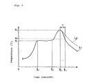
- a change in temperature of a solder paste within reflow apparatus 1 with reference to Fig. 4.
- the vertical axis represents the temperature (°C) of a solder paste near a lead of an electronic part on PCB 3; and the horizontal axis represents the time (seconds).
- a solid line L 1 indicates a solder paste temperature change curve when using reflow apparatus 1 according to the first embodiment, and a broken line L 2 indicates a solder paste temperature change curve when using a conventional reflow apparatus.
- PCB 3 which has a solder paste printed thereon and electronic parts mounted on one side thereof is introduced into furnace 6 of reflow apparatus 1.
- PCB 3 introduced into furnace 6 is conveyed along the conveying path by conveyer mechanism 11, and the solder paste on PCB 3 is heated by heating units 12.
- solder paste on PCB 3 introduced into furnace 6 from inlet port 7 by conveyer mechanism 11 is heated by pre-heaters 16 of heating units 12 to approximately 150 °C to 170 °C (temperature x 1 ), for example, after 135 to 145 seconds (time t 1 ) from the introduction of PCB 3.
- the solder paste on PCB 3 heated to approximately temperature x 1 is maintained at this temperature by pre-heaters 16 for 80 to 100 seconds.
- the pre-heating is completed after 215 to 245 seconds (time t 2 ) from the introduction of PCB 3, and PCB 3 maintained at temperature x 1 is further conveyed by conveyer mechanism 11.
- the solder paste on PCB 3 is heated to approximately 210 °C (temperature x 3 ) or higher and melted by heaters 17 of heating units 12 after 265 to 305 seconds (time t 3 ) from the introduction of PCB 3.
- PCB 3 is further conveyed by conveyer mechanism 11, and the melted solder paste on PCB 3 is cooled down to approximately 190 °C (temperature x 2 ) or lower by cooling fans 18 of cooling units 13 in approximately 13 seconds (cooling time T).
- cooling units 13 cool down and solidify the solder paste on PCB 3 at a cooling speed of 1.5 °C/second or higher.
- Cooled PCB 3 is removed from outlet port 8 after 278 to 318 seconds (time t 4 ) from the introduction, and left at a room temperature for a predetermined time.
- PCB 3 is prevented from the formation of low-strength/low-melting point alloy layers on the interfaces of lands and solders due to the segregation of Sn-Zn-Pb (the melting point of which is 177 °C), and Sn-Pb-Bi (the melting point of which is 98 °C) made from Pb, which is a component of the plating films on the leads, and Sn-Zn-Bi, which are components of the Sn-Zn-Bi based solder. Consequently, the electronic parts are securely bonded on PCB 3.
- Sn-Zn-Pb the melting point of which is 177 °C
- Sn-Pb-Bi the melting point of which is 98 °C
- the conventional reflow processing cools down and solidifies the solder paste on PCB 3 by cooling units 13 at a cooling speed of approximately 0.5 to 0.8 °C/second.
- Sn-Zn-Pb and Sn-Pb-Bi segregate on interfaces between lands and solders, resulting in the formation of low-strength/low-melting point alloy layers on the interfaces.
- the reflow processing according to the first embodiment rapidly cools down and solidifies the solder paste at a cooling speed approximately twice or three times higher than the conventional reflow processing, as can be appreciated from the slope of the cooling curve L 1 presenting the cooling speed, which is more abrupt than the slope of the cooling curve L 2 according to the conventional reflow processing.
- Pb diffuses from the plating films on the leads of the electronic parts mounted on PCB 3, so that the solder paste can be solidified in the uniform composition before Sn-Zn-Pb and Sn-Pb-Bi segregate on the interfaces between lands and solders.
- furnace 6 of reflow apparatus 1 receives PCB 3 which has electronic parts mounted on one side thereof by reflowing in the preceding step and has electronic parts loaded on a solder paste printed on the other side thereof.
- the reflow processing is applied to the other side of PCB 3 in a manner similar to the aforementioned reflow processing on the one side of PCB 3 within furnace 6 of reflow apparatus 1. Consequently, the electronic parts mounted on the other side of PCB 3 are also bonded with a sufficient strength ensured by the solder, thereby preventing defective soldering.
- the solder paste on leads of electronic parts which have been previously mounted by reflowing on the one side of PCB 3 is also cooled down rapidly by cooling unit 13 at a cooling speed of 1.5 °C/second or higher. Therefore, even if the solder paste on the one side of PCB 3 is melted again by the heating of heating units 12, the solder paste is rapidly cooled down and solidified. As such, the electronic parts previously mounted on the one side of PCB 3 are bonded with a sufficient strength ensured by the solder, thereby preventing defective soldering even after PCB 3 has undergone the reflow processing on the other side thereof.
- the cooling speed of cooling units 13 is set to 1.5 °C/second or higher to prevent the segregation of Sn-Zn-Pb (the melting point of which is 177 °C), and Sn-Pb-Bi (the melting point of which is 98 °C).
- the segregation of Sn-Pb-Bi can be further suppressed by reducing the content of Bi in the Sn-Zn-Bi based solder to less than 3 wt%.
- a reflow apparatus herein used is a conventional reflow apparatus which cools down and solidifies a melted solder paste at a cooling speed on the order of 0.5 °C/second to 0.8 °C/second. Also, in Fig.
- the topmost figure shows an enlarged cross-sectional view of a portion of the lead of the electronic part connected by soldering
- a figure labeled “SEM” is a further enlarged cross-sectional view of a portion (PAD) surrounded by a dotted line in the topmost figure.
- Figures labeled the names of elements such as "Pb” show whether or not associated elements exist in a region shown by the figure labeled "SEM", wherein the elements exist in portions which appear whitish in the figures.
- FIG. 6 there is shown an enlarged photomicrograph of the portion of the lead of the electronic part connected by soldering after the second reflow processing is performed on the other side of PCB.
- two or more kinds of solder powders are blended into a paste form when an Sn-Zn-Bi based solder paste is created to adjust the content of Bi to less than 3 wt% in the Sn-Zn-Bi based solder and to increase the temperature difference between the liquidus and solidus.
- solder paste for creating an Sn-Zn-Bi based solder paste containing 2 % of Bi, two kinds of solder powders are blended into a paste form, for example, in the following weight ratio to create the solder paste:
- solder paste for creating an Sn-Zn-Bi based solder paste containing 1 % of Bi, two kinds of solder powders are blended into a paste form, for example, in the following weight ratio to create the solder paste:
- solder pastes created in the foregoing examples contain 1 % or 2 % of Bi, they exhibit the same temperature difference between the liquidus and solidus as that of Sn-8Zn-3Bi, thus making it possible to reduce the amount of solder when melts at the beginning. Since this can reduce the surface tension of the solder, it is possible to suppress the chip build-up defect. It should be understood that the foregoing compositions and weight ratios are illustrative in any sense, and similar effects to those can be produced as well with other compositions or weight ratios.
- the first embodiment sets the cooling speed of 1.5 °C/second or higher for cooling units 13 of reflow apparatus 1 to rapidly cool down and solidify a melted solder paste before the segregation of Sn-Zn-Pb (the melting point of which is 177 °C), and Sn-Pb-Bi (the melting point of which is 98 °C).
- the first embodiment suppresses the formation of low-strength/low-melting point alloy layers due to the segregation of Sn-Pb-Bi and Sn-Zn-Pb on interfaces of lands and solders, so that the quality and reliability of solder-based bonding are ensured for electronic parts mounted on PCB 3.
- solder powders When two or more kinds of solder powders are blended into an Sn-Zn-Bi based solder paste containing less than 3 wt% of Bi, the resulting solder paste exhibits a larger temperature difference between the liquidus and solidus, thereby making it possible to suppress the chip build-up defect.
- the present invention is also suitably applied in a single-side reflow process for mounting electronic parts only on one side of a PCB by reflowing.
- the present invention is also suitably applied for bonding other electronic parts which may contain Pb in locations to which a solder paste is applied.
- a mount structure is manufactured by a reflow/flow composite process for soldering electronic parts by reflowing on one side of PCB 3 and subsequently soldering electronic parts by flowing on the other side of PCB 3.
- a flow apparatus for use in the flow processing according to the second embodiment applies the flow processing to a PCB which has throughholes through which leads of a variety of electronic parts are inserted to load the electronic parts on the PCB.
- a solder for use in the flow processing an Sn-Ag based alloy, an Sn-Cu based alloy, an Sn-Zn based alloy and the like are preferably used from a viewpoint Pb-free promotion.
- electronic parts mounted on the PCB are those electronic parts which have leads covered with a plating film containing Pb.
- flow apparatus 20 for use in the flow processing according to the second embodiment comprises a furnace 21 for performing the flow processing on PCB 3.
- Furnace 21 is provided with inlet port 22 on one end side from which PCB 3 is introduced into furnace 21 for the flow processing; and outlet port 23 on the other end side from which flowed PCB 3 is removed from furnace 21.
- Flow apparatus 20 further comprises conveyer mechanism 24 for conveying PCB 3 within furnace 21; a solder bath 25 for spraying a melted solder, stored therein, toward PCB 3; and a cooling unit 26 for cooling down and solidifying the melted solder on PCB 3.
- Conveyer mechanism 24 comprises carrier 27 on which PCB 3 is carried; and a driving mechanism (not shown) for driving carrier 27 in a direction indicated by an arrow b in Fig. 7 along a conveying path at a predetermined conveying speed.
- the conveying path is provided for the carrier 27 to move from inlet port 22 to outlet port 23 within furnace 21.
- This conveyer mechanism 24 conveys PCB 3, for example, at a conveying speed of approximately 1.0 m/minute.
- Solder bath 25 is arranged below the conveying path within furnace 21.
- This solder bath 25 comprises nozzles 28, 29, such that a melted solder is sprayed toward PCB 3 in a double wave mode which is made up of a jet stream of solder from nozzle 28 (primary jet stream) and a jet stream of solder from nozzle 29 (secondary jet stream).
- Cooling unit 26 is arranged near outlet port 23 along the conveying path within furnace 21.
- This cooling unit 26 can be implemented, for example, using a cooling fan, but any other configuration may be employed as long as it can send cooling air to PCB 3.
- the reflow apparatus and solder paste for use in the reflow processing according to the second embodiment are similar to those used in the aforementioned first embodiment.
- PCB 3 having electronic parts loaded on a solder paste printed on one side thereof in the preceding step is introduced into furnace 6 of reflow apparatus 1 illustrated in Fig. 3.
- PCB 3 introduced into furnace 6 is conveyed by conveyer mechanism 11 along the conveying path, and the solder paste on PCB 3 is heated to its melting point or higher and melted by heating units 12.
- PCB 3 is further conveyed by conveyer mechanism 11, and the melted solder paste on PCB 3 is rapidly cooled down and solidified by cooling units 13 at a cooling speed of 1.5 °C/second or higher to mount the electronic parts on PCB 3.
- furnace 21 of flow apparatus 20 illustrated in Fig. 7 receives PCB 3 which has the electronic parts mounted on the one side thereof by reflowing in the preceding step, and having other electronic parts loaded on the other side with their leads inserted through throughholes of PCB 3 from the one side.
- PCB 3 introduced into furnace 21 is conveyed by conveyer mechanism 24 above solder bath 25 along the conveying path within furnace 21.
- a melted solder is sprayed from nozzles 28, 29 of solder bath 25 toward PCB 3 while the temperature equal to or lower than 170 °C is maintained in portions connected by soldering of the electronic parts mounted on the one side of PCB 3 by reflowing.
- the segregation of Sn-Zn-Pb (the melting point of which is 177 °C) is suppressed by adjusting the cooling speed in the aforementioned reflow processing, but is not fully eliminated, so that a trace of Sn-Zn-Pb exists. For this reason, the temperature equal to or lower than 170 °C is maintained in portions connected by soldering of the electronic parts previously mounted on the one side of PCB 3 during the flow processing to prevent Sn-Zn-Pb existing in very small quantities on the one side of PCB 3 from melting again. This can ensure the quality and reliability of the portions connected by soldering of the electronic parts on the one side of the PCB 3. As described above, the segregation of Sn-Pb-Bi (the melting point of which is 98 °C) can be suppressed by using an Sn-Zn-Bi based solder containing less than 3 wt% of Bi.
- PCB 3 is further conveyed by conveyer mechanism 24, and the melted solder on PCB 3 is cooled down to the melting point or lower and solidified by cooling unit 26, thereby mounting the electronic parts on PCB 3.
- Flow apparatus 30 illustrated in Fig. 8 differs from flow apparatus 20 in Fig. 7 in that cooling unit 31 is additionally provided for cooling down PCB 3 from above.
- This cooling unit 31 can be implemented, for example, using a cooling fan, but any other configuration may be employed as long as it can send cooling air to PCB 3.
- Portions in Fig. 8 similar to those'in Fig. 7 are designated the same reference numerals, and description thereon is omitted.
- the flow processing is performed while cooling unit 31 is blowing cooling air, from above, to portions connected by soldering of electronic parts which have been previously mounted on the one side of PCB 3 by reflowing.
- This prevents the temperature of the portions connected by soldering from rising due to the heat of the solder sprayed from solder bath 25.
- an N2 gas is preferably used as cooling air for preventing the solder stored within solder bath 25 from being oxidized by the cooling air.
- the flow processing is performed with a thermally insulating material applied on the other side of PCB 3 to cover surface mounted part 70 previously mounted on the one side of PCB 3 from the other side. In this way, the heat of the solder sprayed from the nozzles of solder bath 25 is prevented from conducting to portions connected by soldering.
- masking tape 72 is adhered on the other side of PCB 3 as the thermal insulating material to cover surface mounted part 70, and the flow processing is performed in this state.
- a material suitable for masking tape 72 is that having a large thermal capacitance or a low thermal conductivity.
- a paper tape, an aluminum tape or the like may be used for the purpose.
- the flow processing is performed with PCB 3 placed on tray 73 which acts as the thermally insulating material.
- a material suitable for use as tray 73 is that having a large thermal capacity or that having a low thermal conductivity.
- Tray 73 is formed with openings corresponding to throughholes of PCB 3 through which leads of throughhole part 71 extend.
- the thermally insulating materials may be any alternatives other than the aforementioned masking tape and tray, as long as they limit the conduction of heat from the solder sprayed from solder bath 25.
- the second embodiment sets the cooling speed of 1.5 °C/second or higher for cooling units 13 of reflow apparatus 1 during the reflow processing on the one side of PCB 3, thereby suppressing the formation of a low-strength/low-melting point alloy layer due to the segregation of Sn-Zn-Pb (the melting point of which is 177 °C) and Sn-Pb-Bi (the melting point of which is 98 °C). This ensures the quality and reliability of solder-based bonding for electronic parts previously mounted on the one side of PCB 3.
- solder paste when an Sn-Zn-Bi based solder containing less than 3 wt% of Bi is used as a solder paste, it is possible to further suppress the segregation of Sn-Pb-Bi. Furthermore, when two or more kinds of solder powders are blended into an Sn-Zn-Bi based solder paste, the chip build-up defect can be suppressed.
- the second embodiment maintains the temperature equal to or lower than 170 °C in portions connected by soldering of the electronic parts previously mounted by reflowing on the one side of PCB 3 during the flow processing, it is possible to prevent Sn-Zn-Pb existing in very small quantities on the one side of PCB 3 from melting again. This ensures the quality and reliability of solder-based bonding for the electronic parts previously mounted on the one side of PCB 3 even after PCB 3 undergoes the subsequent flow processing on the other side thereof.
- the present invention is also suitably applied for bonding other electronic parts which may contain Pb in locations to which a solder paste is applied.
Landscapes
- Engineering & Computer Science (AREA)
- Manufacturing & Machinery (AREA)
- Microelectronics & Electronic Packaging (AREA)
- Electric Connection Of Electric Components To Printed Circuits (AREA)
Abstract
Description
| Composition | Liquidus | Solidus | Temperature Difference |
| Sn-9Zn | 199 | 199 | 0 |
| Sn-8Zn-1Bi | 199 | 192 | 7 |
| Sn-8Zn-3Bi | 197 | 187 | 10 |
Claims (21)
- A method of manufacturing a mount structure having a printed board and an electronic part mounted on said printed board by soldering, said method comprising the steps of:a) applying a solder paste on said printed board, and loading said electronic part on said printed board through said solder paste;b) heating and melting said solder paste applied on said printed board; andc) forcedly cooling down said melted solder paste at a cooling speed of 1.5 °C/second or higher to solidify said melted solder paste.
- The manufacturing method according to claim 1, wherein said step b) includes heating said solder paste to 210 °C or higher.
- The manufacturing method according to claim 1 or 2, wherein said step c) includes cooling down said solder paste to 190 °C or lower.
- The manufacturing method according to any of claims 1 to 3, wherein said solder paste comprises an Sn-Zn based alloy.
- The manufacturing method according to any of claims 1 to 3, wherein said solder paste comprises an Sn-Zn-Bi based alloy.
- The manufacturing method according to claim 5, wherein said solder paste contains 3 % or less of Bi in said Sn-Zn-Bi based alloy.
- The manufacturing method according to any of claims 1 to 6, wherein said solder paste comprises two kinds or more of solder powders blended into a paste form.
- The manufacturing method according to any of claims 1 to 7, further comprising the step of:wherein said step c) for said second electronic part includes forcedly cooling down the solders on both sides of said printed board, said solders being melted in said step b) for said second electronic part, to solidify said solders.after a first electronic part is mounted on one side of said printed board through said step a), said step b) and said step c), mounting a second electronic part on the other side of said printed board through said step a), said step b) and said step c),
- The manufacturing method according to any of claims 1 to 7, further comprising the steps of:after mounting a first electronic part on one side of said printed board through said step a), said step b) and said step c), loading a second electronic part by inserting leads of said second electronic part through throughholes of said printed board from the one side of said printed board; andmounting said second electronic part by flowing while maintaining the solder applied on the one side of said printed board at temperatures of 170 °C or lower.
- The manufacturing method according to claim 9, wherein said flow process includes adjusting the temperature of said solder by sending cooling air to said solder applied on one side of said printed board.
- The manufacturing method according to claim 10, wherein said cooling air comprises an N2 gas.
- The manufacturing method according to claim 9, wherein said flow process includes adjusting the temperature of said solder by disposing a thermally insulating material on the other side to cover the electronic part mounted on the one side of said printed board from the other side of said printed board.
- The manufacturing method according to claim 12, wherein said thermally insulating material comprises a masking tape adhered on said printed board.
- The manufacturing method according to claim 12, wherein said thermally insulating material comprises a tray on which said printed board is placed.
- A mount structure comprising:a printed board; andan electronic part bonded to said printed board by a solidified solder paste cooled down from a melted state at a cooling speed of 1.5 °C/second or higher.
- The mount structure according to claim 15, wherein said solder paste comprises an Sn-Zn based alloy.
- The mount structure according to claim 15, wherein said solder paste comprises an Sn-Zn-Bi based alloy.
- The mount structure according to claim 17, wherein said solder paste contains 3 % or less of Bi in said Sn-Zn-Bi based alloy.
- The mount structure according to any of claims 15 to 18, wherein said solder paste comprises two kinds or more of solder powders blended into a paste form.
- The mount structure according to any of claims 15 to 19, comprising:wherein the solder on said one side of said printed board is cooled down together at said cooling speed when said solder paste on said other side of said printed board is cooled down at said cooling speed.a first electronic part bonded on one side of said printed board by said solder paste cooled down and solidified from the melted state at said cooling speed; anda second electronic part bonded on the other side of said printed board by said solder paste cooled down and solidified from the melted state at said cooling speed after said first electronic part is bonded on said one side of said printed board,
- The mount structure according to any of claims 15 to 19, comprising:a first electronic part bonded on one side of said printed board by said solder paste cooled down and solidified from the melted state at said cooling speed; anda second electronic part mounted on the other side of said printed board, said second electronic part loaded on said other side with its leads inserted through throughhole of said printed board from said one side, and bonded to said other side by flowing while maintaining the solder on said one side at temperatures of 170 °C or lower, after said first electronic part is bonded to said one side.
Applications Claiming Priority (4)
| Application Number | Priority Date | Filing Date | Title |
|---|---|---|---|
| JP2001166970 | 2001-06-01 | ||
| JP2001166970 | 2001-06-01 | ||
| JP2002048026 | 2002-02-25 | ||
| JP2002048026A JP2003051671A (en) | 2001-06-01 | 2002-02-25 | Manufacturing method of mounting structure and mounting structure |
Publications (3)
| Publication Number | Publication Date |
|---|---|
| EP1295665A2 true EP1295665A2 (en) | 2003-03-26 |
| EP1295665A3 EP1295665A3 (en) | 2004-09-15 |
| EP1295665B1 EP1295665B1 (en) | 2006-07-19 |
Family
ID=26616218
Family Applications (1)
| Application Number | Title | Priority Date | Filing Date |
|---|---|---|---|
| EP02011614A Expired - Lifetime EP1295665B1 (en) | 2001-06-01 | 2002-05-28 | Method of manufacturing mount structure without introducing degraded bonding strength of electronic parts due to segregation of low-strength/low-melting point alloy |
Country Status (7)
| Country | Link |
|---|---|
| US (1) | US6915942B2 (en) |
| EP (1) | EP1295665B1 (en) |
| JP (1) | JP2003051671A (en) |
| KR (1) | KR100593774B1 (en) |
| CN (1) | CN100340141C (en) |
| DE (1) | DE60213173T2 (en) |
| TW (1) | TW551018B (en) |
Cited By (1)
| Publication number | Priority date | Publication date | Assignee | Title |
|---|---|---|---|---|
| FR2854761A1 (en) * | 2003-05-05 | 2004-11-12 | Sagem | Connection terminal fixing method for e.g. modem card, involves depositing two sets of solder studs at level of respective cavity and contact zones, installing electronic components and brazing terminal by reflow of studs |
Families Citing this family (9)
| Publication number | Priority date | Publication date | Assignee | Title |
|---|---|---|---|---|
| JP2003051671A (en) * | 2001-06-01 | 2003-02-21 | Nec Corp | Manufacturing method of mounting structure and mounting structure |
| US7026582B2 (en) * | 2003-05-07 | 2006-04-11 | Visteon Global Technologies, Inc. | Vector transient reflow of lead free solder for controlling substrate warpage |
| JP4040644B2 (en) * | 2005-07-28 | 2008-01-30 | シャープ株式会社 | Method for manufacturing solder mounting structure and solder mounting method |
| DE102005039829A1 (en) * | 2005-08-22 | 2007-03-08 | Endress + Hauser Gmbh + Co. Kg | Method for soldering SMD components, printed circuit board and reflow soldering oven |
| JP5652689B2 (en) * | 2008-09-24 | 2015-01-14 | 株式会社弘輝 | Manufacturing method of electronic component bonded structure and electronic component bonded structure obtained by the manufacturing method |
| CN102131352A (en) * | 2010-01-13 | 2011-07-20 | 鸿富锦精密工业(深圳)有限公司 | Method for manufacturing printed circuit board (PCB) |
| WO2018061207A1 (en) * | 2016-09-30 | 2018-04-05 | 富士機械製造株式会社 | Machine for performing work on substrate, and insertion method |
| JP6849909B2 (en) * | 2017-02-07 | 2021-03-31 | 富士通株式会社 | Soldering method, soldering equipment, and method of keeping the solder wet of the jet nozzle |
| CN111975313A (en) * | 2020-08-07 | 2020-11-24 | 梁华娇 | Pop can bottom installation equipment |
Family Cites Families (54)
| Publication number | Priority date | Publication date | Assignee | Title |
|---|---|---|---|---|
| JPS60124947A (en) * | 1983-12-12 | 1985-07-04 | Nippon Telegr & Teleph Corp <Ntt> | Reflow bonding method |
| JPS6254996A (en) * | 1985-09-04 | 1987-03-10 | アルプス電気株式会社 | Mounting of electronic component |
| DE3720912A1 (en) * | 1986-07-03 | 1988-01-07 | Licentia Gmbh | METHOD AND ARRANGEMENT FOR REFLOW-SOLDERING AND REFLOW-DESOLDERING CIRCUIT BOARDS |
| JPH0666544B2 (en) | 1988-06-11 | 1994-08-24 | 太陽誘電株式会社 | Circuit board manufacturing method |
| JP2866392B2 (en) | 1989-05-24 | 1999-03-08 | 株式会社タムラ製作所 | Soldering method |
| JPH03268386A (en) | 1990-03-16 | 1991-11-29 | Sharp Corp | Method of mounting component on double-sided printed wiring board |
| JP2509373B2 (en) | 1990-07-25 | 1996-06-19 | 権士 近藤 | Reflow soldering method and device for printed circuit board |
| JPH0548376A (en) | 1991-08-20 | 1993-02-26 | Murata Mfg Co Ltd | Piezoelectric component |
| JP3225979B2 (en) | 1992-09-30 | 2001-11-05 | ソニー株式会社 | Electronic circuit manufacturing method |
| US5433368A (en) * | 1992-11-10 | 1995-07-18 | Spigarelli; Donald J. | Soldering system |
| CA2131256A1 (en) * | 1993-09-07 | 1995-03-08 | Dongkai Shangguan | Lead-free solder alloy |
| JPH0878837A (en) | 1994-09-06 | 1996-03-22 | Matsushita Electric Ind Co Ltd | Mounting soldering method and printed circuit board with mounting solder |
| US5560531A (en) * | 1994-12-14 | 1996-10-01 | O.K. Industries, Inc. | Reflow minioven for electrical component |
| KR0156649B1 (en) * | 1995-05-19 | 1998-11-16 | 서상기 | The solder alloy of sn-zn-bi-sb for pb free |
| JPH0929480A (en) | 1995-07-19 | 1997-02-04 | Fujitsu Ltd | Solder paste |
| JP3243684B2 (en) | 1995-09-12 | 2002-01-07 | シャープ株式会社 | Device mounting structure |
| CN1087994C (en) | 1995-09-29 | 2002-07-24 | 松下电器产业株式会社 | Lead-free solder |
| JPH09266373A (en) | 1996-01-25 | 1997-10-07 | Fujitsu Ltd | Electronic component, joining method thereof, and circuit board |
| JPH09206983A (en) | 1996-02-02 | 1997-08-12 | Sony Corp | Solder material |
| JP3643008B2 (en) | 1996-02-09 | 2005-04-27 | 松下電器産業株式会社 | Soldering method |
| JP3220635B2 (en) * | 1996-02-09 | 2001-10-22 | 松下電器産業株式会社 | Solder alloy and cream solder |
| DE19615338C2 (en) * | 1996-04-18 | 1998-08-20 | Helmut W Leicht | Process for cooling soldered goods |
| JPH09326554A (en) * | 1996-06-06 | 1997-12-16 | Matsushita Electric Ind Co Ltd | Solder alloy of electrode for joining electronic parts and soldering method |
| US6231691B1 (en) * | 1997-02-10 | 2001-05-15 | Iowa State University Research Foundation, Inc. | Lead-free solder |
| US5928404A (en) * | 1997-03-28 | 1999-07-27 | Ford Motor Company | Electrical solder and method of manufacturing |
| JP3688429B2 (en) * | 1997-04-25 | 2005-08-31 | 株式会社東芝 | Electronic component mounting substrate and electronic component mounting substrate |
| JPH1126924A (en) | 1997-07-01 | 1999-01-29 | Sumitomo Wiring Syst Ltd | Method for soldering flexible printed wiring board and jig for soldering the same |
| JPH11138292A (en) | 1997-11-10 | 1999-05-25 | Showa Denko Kk | Lead-free solder paste |
| JPH11245079A (en) | 1998-02-27 | 1999-09-14 | Toshiba Corp | Metal powder for solder paste and method for producing the same |
| JP3414263B2 (en) | 1998-06-04 | 2003-06-09 | 株式会社日立製作所 | Manufacturing method of electronic circuit board |
| US6204490B1 (en) | 1998-06-04 | 2001-03-20 | Hitachi, Ltd. | Method and apparatus of manufacturing an electronic circuit board |
| US7771547B2 (en) * | 1998-07-13 | 2010-08-10 | Board Of Trustees Operating Michigan State University | Methods for producing lead-free in-situ composite solder alloys |
| US6214131B1 (en) * | 1998-10-29 | 2001-04-10 | Agilent Technologies, Inc. | Mixed solder pastes for low-temperature soldering process |
| JP2000188464A (en) * | 1998-12-21 | 2000-07-04 | Senju Metal Ind Co Ltd | Automatic soldering device |
| FR2787737B1 (en) * | 1998-12-23 | 2001-01-19 | Commissariat Energie Atomique | SOLDERING COMPOSITION, METHOD FOR ASSEMBLING PARTS OF ALUMINA-BASED MATERIALS BY REFRACTORY BRAZING WITH SAID SOLDERING COMPOSITION, ASSEMBLY AND REFRACTORY JOINT THUS OBTAINED |
| US6095403A (en) * | 1999-01-22 | 2000-08-01 | International Business Machines Corporation | Circuit board component retention |
| JP2000244108A (en) | 1999-02-22 | 2000-09-08 | Senju Metal Ind Co Ltd | Soldering of printed board, soldering equipment for printed board, and cooling equipment therefor |
| JP2001007507A (en) | 1999-06-25 | 2001-01-12 | Fujitsu Ltd | Reflow equipment |
| JP2001244123A (en) * | 2000-02-28 | 2001-09-07 | Kawatetsu Mining Co Ltd | Surface mount type planar magnetic element and method of manufacturing the same |
| JP4332281B2 (en) | 2000-04-26 | 2009-09-16 | 株式会社日立製作所 | Electronic device manufacturing method and soldering apparatus |
| JP2001358456A (en) | 2000-06-12 | 2001-12-26 | Hitachi Ltd | Electronic devices connected using lead-free solder |
| US6617195B1 (en) * | 2000-07-24 | 2003-09-09 | Advanced Micro Devices, Inc. | Method of reflowing organic packages using no-clean flux |
| JP2002043734A (en) * | 2000-07-24 | 2002-02-08 | Senju Metal Ind Co Ltd | Method and apparatus for soldering printed circuit board |
| US6648216B2 (en) * | 2000-08-21 | 2003-11-18 | Matsushita Electric Industrial Co., Ltd. | Process and apparatus for flow soldering |
| JP4577974B2 (en) * | 2000-10-31 | 2010-11-10 | パナソニック株式会社 | Flow soldering method and apparatus |
| FR2818088B1 (en) * | 2000-12-11 | 2003-02-28 | Air Liquide | METHOD FOR PRODUCING A BRAZING BETWEEN METAL BALLS OF AN ELECTRONIC COMPONENT AND HOST RANGES OF A CIRCUIT AND BRAZING OVEN FOR CARRYING OUT THIS PROCESS |
| JP4656275B2 (en) * | 2001-01-15 | 2011-03-23 | 日本電気株式会社 | Manufacturing method of semiconductor device |
| JP2003051671A (en) * | 2001-06-01 | 2003-02-21 | Nec Corp | Manufacturing method of mounting structure and mounting structure |
| DE10133217A1 (en) * | 2001-07-09 | 2003-01-23 | Seho Systemtechnik Gmbh | Method and device for soldering electrical components to plastic film |
| JP4073183B2 (en) * | 2001-08-01 | 2008-04-09 | 株式会社日立製作所 | Mixed mounting method using Pb-free solder and mounted product |
| US6610559B2 (en) * | 2001-11-16 | 2003-08-26 | Indium Corporation Of America | Integrated void-free process for assembling a solder bumped chip |
| US6642485B2 (en) * | 2001-12-03 | 2003-11-04 | Visteon Global Technologies, Inc. | System and method for mounting electronic components onto flexible substrates |
| JP2003198117A (en) * | 2001-12-28 | 2003-07-11 | Matsushita Electric Ind Co Ltd | Soldering method and joint structure |
| US6805974B2 (en) * | 2002-02-15 | 2004-10-19 | International Business Machines Corporation | Lead-free tin-silver-copper alloy solder composition |
-
2002
- 2002-02-25 JP JP2002048026A patent/JP2003051671A/en active Pending
- 2002-05-22 TW TW091110754A patent/TW551018B/en active
- 2002-05-28 DE DE60213173T patent/DE60213173T2/en not_active Expired - Lifetime
- 2002-05-28 EP EP02011614A patent/EP1295665B1/en not_active Expired - Lifetime
- 2002-05-29 US US10/156,098 patent/US6915942B2/en not_active Expired - Fee Related
- 2002-05-31 KR KR1020020030515A patent/KR100593774B1/en not_active Expired - Fee Related
- 2002-06-03 CN CNB021221790A patent/CN100340141C/en not_active Expired - Fee Related
Cited By (1)
| Publication number | Priority date | Publication date | Assignee | Title |
|---|---|---|---|---|
| FR2854761A1 (en) * | 2003-05-05 | 2004-11-12 | Sagem | Connection terminal fixing method for e.g. modem card, involves depositing two sets of solder studs at level of respective cavity and contact zones, installing electronic components and brazing terminal by reflow of studs |
Also Published As
| Publication number | Publication date |
|---|---|
| DE60213173D1 (en) | 2006-08-31 |
| JP2003051671A (en) | 2003-02-21 |
| TW551018B (en) | 2003-09-01 |
| EP1295665B1 (en) | 2006-07-19 |
| CN100340141C (en) | 2007-09-26 |
| CN1396802A (en) | 2003-02-12 |
| US6915942B2 (en) | 2005-07-12 |
| KR100593774B1 (en) | 2006-07-03 |
| KR20020092230A (en) | 2002-12-11 |
| US20030005581A1 (en) | 2003-01-09 |
| EP1295665A3 (en) | 2004-09-15 |
| DE60213173T2 (en) | 2007-07-12 |
Similar Documents
| Publication | Publication Date | Title |
|---|---|---|
| US20080179379A1 (en) | Solder joint structure, soldering method, and electronic-component manufacturing apparatus using the same structure and the method | |
| US6871775B2 (en) | Process for soldering and connecting structure | |
| US5415944A (en) | Solder clad substrate | |
| US6915942B2 (en) | Method of manufacturing mount structure without introducing degraded bonding strength of electronic parts due to segregation of low-strength/low-melting point alloy | |
| US8961709B1 (en) | Solder paste | |
| US6929973B2 (en) | Method of packaging electronic components with high reliability | |
| KR100671394B1 (en) | Reflow soldering method and mixed mounting method and mixed mounting structure using PPS-free solder alloy | |
| JP2004241542A (en) | Soldering method, parts joined by the soldering method, and joined joint structure | |
| US20030116352A1 (en) | Wave soldering method using lead-free solder, apparatus therefor, and wave-soldered assembly | |
| US7413110B2 (en) | Method for reducing stress between substrates of differing materials | |
| JP2002359459A (en) | Electronic component mounting method, printed wiring board, and mounting structure | |
| JPH11245079A (en) | Metal powder for solder paste and method for producing the same | |
| JP2004158898A (en) | Construction method of mounting structure, and mounting structure | |
| US5623127A (en) | Single alloy solder clad substrate | |
| JP2000332403A (en) | Electronic component mounting structure and electronic component mounting method | |
| JP2002141658A (en) | Flow soldering method and apparatus | |
| JP2003198116A (en) | Soldering method and joint structure | |
| JP2003069214A (en) | Manufacturing method of electronic circuit board using lead-free solder | |
| JP2004319726A (en) | Soldering connection, soldering method thereof, and electronic component manufacturing apparatus using the same | |
| JPH05259632A (en) | Printed wiring board and manufacture thereof | |
| JP2004311679A (en) | Soldering method and its printed wiring board | |
| JP2005057117A (en) | Soldering method, joint structure, and electric / electronic component | |
| JPH01268186A (en) | Board device using surface mounting electronic component | |
| JPH01274492A (en) | Manufacture of substrate device using non-eutectic solder | |
| JPH04298097A (en) | Mounting method for electronic component using low melting point solder |
Legal Events
| Date | Code | Title | Description |
|---|---|---|---|
| PUAI | Public reference made under article 153(3) epc to a published international application that has entered the european phase |
Free format text: ORIGINAL CODE: 0009012 |
|
| AK | Designated contracting states |
Kind code of ref document: A2 Designated state(s): AT BE CH CY DE DK ES FI FR GB GR IE IT LI LU MC NL PT SE TR |
|
| AX | Request for extension of the european patent |
Extension state: AL LT LV MK RO SI |
|
| PUAL | Search report despatched |
Free format text: ORIGINAL CODE: 0009013 |
|
| AK | Designated contracting states |
Kind code of ref document: A3 Designated state(s): AT BE CH CY DE DK ES FI FR GB GR IE IT LI LU MC NL PT SE TR |
|
| AX | Request for extension of the european patent |
Extension state: AL LT LV MK RO SI |
|
| RIC1 | Information provided on ipc code assigned before grant |
Ipc: 7B 23K 1/012 A Ipc: 7H 05K 3/34 B Ipc: 7B 23K 1/008 B Ipc: 7B 23K 35/26 B Ipc: 7B 23K 1/00 B |
|
| 17P | Request for examination filed |
Effective date: 20040805 |
|
| 17Q | First examination report despatched |
Effective date: 20050121 |
|
| AKX | Designation fees paid |
Designated state(s): DE FR GB |
|
| GRAP | Despatch of communication of intention to grant a patent |
Free format text: ORIGINAL CODE: EPIDOSNIGR1 |
|
| GRAS | Grant fee paid |
Free format text: ORIGINAL CODE: EPIDOSNIGR3 |
|
| GRAA | (expected) grant |
Free format text: ORIGINAL CODE: 0009210 |
|
| AK | Designated contracting states |
Kind code of ref document: B1 Designated state(s): DE FR GB |
|
| REG | Reference to a national code |
Ref country code: GB Ref legal event code: FG4D |
|
| REF | Corresponds to: |
Ref document number: 60213173 Country of ref document: DE Date of ref document: 20060831 Kind code of ref document: P |
|
| ET | Fr: translation filed | ||
| PLBE | No opposition filed within time limit |
Free format text: ORIGINAL CODE: 0009261 |
|
| STAA | Information on the status of an ep patent application or granted ep patent |
Free format text: STATUS: NO OPPOSITION FILED WITHIN TIME LIMIT |
|
| 26N | No opposition filed |
Effective date: 20070420 |
|
| REG | Reference to a national code |
Ref country code: DE Ref legal event code: R082 Ref document number: 60213173 Country of ref document: DE Representative=s name: VOSSIUS & PARTNER PATENTANWAELTE RECHTSANWAELT, DE Effective date: 20110929 Ref country code: DE Ref legal event code: R081 Ref document number: 60213173 Country of ref document: DE Owner name: NEC PERSONAL COMPUTERS, LTD., JP Free format text: FORMER OWNER: NEC CORP., TOKYO, JP Effective date: 20110929 |
|
| REG | Reference to a national code |
Ref country code: FR Ref legal event code: TP Owner name: NEC PERSONAL COMPUTERS, LTD, JP Effective date: 20111024 |
|
| REG | Reference to a national code |
Ref country code: GB Ref legal event code: 732E Free format text: REGISTERED BETWEEN 20120223 AND 20120229 |
|
| PGFP | Annual fee paid to national office [announced via postgrant information from national office to epo] |
Ref country code: GB Payment date: 20140528 Year of fee payment: 13 |
|
| PGFP | Annual fee paid to national office [announced via postgrant information from national office to epo] |
Ref country code: FR Payment date: 20140509 Year of fee payment: 13 Ref country code: DE Payment date: 20140521 Year of fee payment: 13 |
|
| REG | Reference to a national code |
Ref country code: DE Ref legal event code: R119 Ref document number: 60213173 Country of ref document: DE |
|
| GBPC | Gb: european patent ceased through non-payment of renewal fee |
Effective date: 20150528 |
|
| REG | Reference to a national code |
Ref country code: FR Ref legal event code: ST Effective date: 20160129 |
|
| PG25 | Lapsed in a contracting state [announced via postgrant information from national office to epo] |
Ref country code: DE Free format text: LAPSE BECAUSE OF NON-PAYMENT OF DUE FEES Effective date: 20151201 Ref country code: GB Free format text: LAPSE BECAUSE OF NON-PAYMENT OF DUE FEES Effective date: 20150528 |
|
| PG25 | Lapsed in a contracting state [announced via postgrant information from national office to epo] |
Ref country code: FR Free format text: LAPSE BECAUSE OF NON-PAYMENT OF DUE FEES Effective date: 20150601 |