EP1293909A1 - Controle d'accès dynamique d'une fonction à une ressource collective. - Google Patents
Controle d'accès dynamique d'une fonction à une ressource collective. Download PDFInfo
- Publication number
- EP1293909A1 EP1293909A1 EP02078450A EP02078450A EP1293909A1 EP 1293909 A1 EP1293909 A1 EP 1293909A1 EP 02078450 A EP02078450 A EP 02078450A EP 02078450 A EP02078450 A EP 02078450A EP 1293909 A1 EP1293909 A1 EP 1293909A1
- Authority
- EP
- European Patent Office
- Prior art keywords
- function
- access
- value
- latency
- called
- Prior art date
- Legal status (The legal status is an assumption and is not a legal conclusion. Google has not performed a legal analysis and makes no representation as to the accuracy of the status listed.)
- Granted
Links
Images

Classifications
-
- G—PHYSICS
- G06—COMPUTING OR CALCULATING; COUNTING
- G06F—ELECTRIC DIGITAL DATA PROCESSING
- G06F13/00—Interconnection of, or transfer of information or other signals between, memories, input/output devices or central processing units
- G06F13/14—Handling requests for interconnection or transfer
- G06F13/36—Handling requests for interconnection or transfer for access to common bus or bus system
- G06F13/362—Handling requests for interconnection or transfer for access to common bus or bus system with centralised access control
-
- G—PHYSICS
- G06—COMPUTING OR CALCULATING; COUNTING
- G06F—ELECTRIC DIGITAL DATA PROCESSING
- G06F13/00—Interconnection of, or transfer of information or other signals between, memories, input/output devices or central processing units
- G06F13/14—Handling requests for interconnection or transfer
- G06F13/16—Handling requests for interconnection or transfer for access to memory bus
- G06F13/1605—Handling requests for interconnection or transfer for access to memory bus based on arbitration
Definitions
- the invention relates to a method for controlling the access of a function to a resource. collective.
- the invention can be applied, for example, in a device for processing data with multiple functions that may have memory access needs very different.
- a circuit comprising at least one calculation function such as a processor, in link with data processing blocks which can be audio, video or graphics is an example of such a device.
- Some data processing blocks audio, video or graphics require real-time behavior (graphics units ...) and therefore fairly continuous memory accesses.
- graphics units graphics
- other processing blocks of data can be satisfied with less continuous memory access, as long as over a period given a certain amount of access is guaranteed to them.
- a calculation function accesses generally in memory by bursts ("burst of access" in English) for, for example, fill its cache memory. If access to the calculation functions is not limited, the data processing is blocked. This is particularly a problem for the processes in real time. It is therefore necessary to control the memory accesses of the calculation function.
- Access to the collective resource can be managed using an interface.
- the interface implements an access scheme on two levels, that of the access itself and that of the cycle.
- the invention relates to access arbitration.
- a possible access scheme limits the accesses of a function to the memory by preventing accesses of the function that are too close together.
- Practically a register is programmed in the interface to impose a minimum number of clock cycles between two successive accesses. If the number of cycles between two accesses is less than the value entered in the register, the access will be deferred until this value is reached.
- the function for example a calculation function, having requested access will then wait several cycles before admission.
- the value entered in the register depends on the needs of the other functions with which the memory is shared.
- This access scheme is mentioned in European patent application EP0921468. This patent application relates to a memory access control circuit in which is implemented in particular a register containing a latency quantity imposing a fixed number of cycles between two successive accesses to a collective resource.
- An object of the invention is to allow dynamic exploitation of the band bandwidth.
- the invention takes the following aspects into consideration.
- the calculation functions have generally specific memory access needs. Most of the time, a function does not need to access memory because the necessary data is stored in another memory which is specific to it such as a cache memory for example. Of from time to time she needs to access instructions that are not in memory hidden. In this case the calculation function will require a burst of access to the external memory to complete its cache. The access need of a given function can thus vary in the time critically.
- the fixed access scheme described above distributes the capacity access offered by the collective resource among the different functions in a way predetermined. This results in a long wait for the calculation function, in this example, to access the necessary data.
- the invention is concerned with access to the resource collective of functions for which no access is required for a certain time until an access burst is required.
- the invention makes it possible to take into account the previous accesses of the function to assign an access authorization or not. Indeed, the invention takes into account the number of accesses of the calculation function in the near past by imposing a number of cycles between two successive accesses greater than the latency when this number of accesses in the near past is greater than one number given.
- the method according to the invention adds to a fixed access condition a condition of access to the memory making it possible to optimize the short bursts of access which represent the majority of the accesses of the calculation functions.
- the new condition is calculated so as to offer on average as much access to the calculation function as in the case of a fixed access scheme optimized for proper functioning of the other functions.
- the latency quantity which determines, like a fixed access scheme, the shortest interval between two successive accesses, is less than that of the fixed access scheme.
- the present invention also relates to a computer program for implementing a method according to the invention, a memory access control circuit having registers and comparison means for implementing a method according to the invention and a data processing device in which is advantageously implemented a circuit according to the invention.
- FIG. 1 is a diagram of a signal processing device according to the invention. This figure relates to a preferred embodiment in which the invention can be advantageously implemented.
- the function to which access is controlled according to the invention is a calculation function such as a CPU processor.
- a collective resource, here a memory MEM is shared by the CPU function with other functions called AVG.
- functions are audio, video or graphic data processing AVG [1] to AVG [N].
- a CDU unit realizes a first interface between these functions and a SIF access control interface MEM memory.
- the CPU sends its requests on a connection bus BUS device to a SIF interface.
- MEM memory can be all kinds of memory that can be shared between different functions, for example a dynamic memory (SDRAM, DRAM), static memory (SRAM), non-volatile memory (FLASH, ROM, ...) or a mass storage unit (HDD, CD, 7) ...
- SDRAM dynamic memory
- DRAM static memory
- SRAM static memory
- FLASH non-volatile memory
- HDD mass storage unit
- FIG. 2 illustrates the operation of the memory access control method according to the invention.
- FIG. 2 describes a preferred embodiment advantageously implemented in a SIF interface as shown in Figure 1.
- the step of imposing the latency is carried out by comparing to zero a first value decremented by one at each memory cycle where the calculation element does not access the memory and wherein said first value is greater than zero, said first value being incremented by a quantity called latency each time the calculation element is accessed.
- the step of imposing the penalty is carried out by a comparison with a fixed magnitude different from zero, called deposit, calculated as a function of the given number of successive accesses, of a second value decremented by one at each memory cycle where the calculation element does not access the memory and where said second value is greater than zero, said second value being incremented by a quantity called penalty each time the calculation element is accessed.
- the authorization for access of the calculation element to the memory on request of the calculation element is granted if said first value is zero and if said second value is less than or equal to the deposit .
- the principle according to the invention can practically be implemented in a circuit for controlling access to a function of a collective resource by the use of three configuration registers each containing a configuration quantity : ACC deposit, LAT latency and PEN penalty.
- the invention also uses two provisional registers REG1 and REG2 containing the decremented values of 1, when they are not already zero, at each cycle where the processor does not access the memory.
- the method according to the invention is regulated by a clock CLK which triggers a series of tests at each cycle as described in FIG. 2.
- a first test T1 compares the value contained in the register REG1 to zero. In the event that this value REG1 is not zero, access by the processor CPU to the memory MEM cannot in all cases be authorized. It therefore does not matter at this stage whether a request has been made by the processor. The request is then hidden. On the other hand, it should be noted that the penalty PEN being greater than the latency LAT, REG2 cannot be zero if REG1 is not.
- the two registers are then decremented by one in A1 then the system waits for the next cycle.
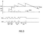
- Figure 3 provides another illustration of the decrementation of the two registers REG1 shown in dotted lines and REG2 shown in solid lines.
- the processor makes an access request as long as REG1 is not zero, this request is not satisfied in the access authorization line GRT before REG1 is zero.
- REG1 the second access request EX1 in FIG. 3.
- the latency LAT thus corresponds to an equivalent of a fixed access scheme as explained in the state of the art. It appears here the need to have a PEN penalty greater than the LAT latency. We will however see that the invention makes it possible to reduce the fixed latency magnitude considerably, which has the advantages explained above for accessing the processor in short bursts.
- REG1 is zero, the preferred embodiment performs a test T2 on the presence of REQ request from the processor.
- a test T4 compares REG2 with the configuration quantity called deposit ACC.
- This configuration quantity is advantageously stored in a configuration register and a simple comparator compares the two values each present in a register. We will see below how this configuration quantity is determined.
- REG2 is greater than the ACC deposit, access is not authorized according to the invention and REG2 is then decremented in A2. The system then waits for the next cycle. This is the case of EX3 in FIG. 3: REG2 is greater than ACC and access is not authorized although REG1 is zero.
- the access of the function to the collective resource is, for example, also authorized by comparison of values of changing registers with values of configuration registers.
- the principle sought remains the same, it concerns the authorization of access according to two conditions: a minimum latency condition and a condition on the presence of access in the near past.
- the registers used by the method according to the invention are advantageously implemented inside the SIF memory interface as shown in FIG. 1.
- the interface then comprises three configuration registers intended for the implementation of the invention and one or preferably two changing registers. In the case where only one register is used, the value registered in this register can be used in tests similar to the tests T by using values memorized with each access of the function and subtractions between the current registered value and the memorized values.
- the interface therefore includes, for example, at least one comparator for the tests of quantities, an adder and a multiplexer to, for example, choose according to the test results, the values (-1, LAT or PEN) which must be added to each register REG1 and REG2.
- the adder-multiplexer pair can thus make it possible to carry out steps A1, A2 and A3.
- a control circuit for implementing the method according to the invention comprises registers, comparators, multiplexers, adders to carry out the operations on the quantities necessary for the invention as described in FIG. 2.
- These elements are conventionally known to those skilled in the art who can arrange them in multiple ways to carry out the method according to the invention.
- Those skilled in the art can use software or hardware elements to implement the method.
- the configuration quantities are defined materially within hardware registers.
- the use of hardware configuration registers makes it possible to be faster than with the use of software means subject to clock speed.
- the invention notably makes it possible to speed up the processes because when the processor CPU has more extensive memory accesses in a shorter time, the speed of the process is increased compared to a fixed access scheme.
- the speed of the access control method is an important outcome in order not to lose the advantage of the invention.
- the present invention can in particular be implemented in devices intended for the processing of digital video data with coding, decoding, compression and repair of the data stream (DVD, recording, digital TV with channel decryption, real-time recording, graphical interface for subtitling ).
- Said devices possibly have interfaces to hard disks to read and write data at the same time, to display elements ...
- These interfaces and device functions are advantageously managed within a circuit specific grouping them together.
- Said circuit is in connection with the receiving peripherals and data mining and with a collective memory used for all circuit functions. It is therefore interesting that part of the circuit manages the interface between the minus one processor present in the data processing circuit and the memory collective. The accesses of said processor will advantageously be controlled according to the invention.
- the memory MEM is here an SDRAM
- the AVG blocks are blocks for processing audio, video and graphic data as described above
- the CPU is advantageously a processor for audio, video and graphic data .
- Such a CPU sends macro commands in a predefined form comprising a request, an address and a command.
- the SIF regularly receives macro-commands resulting from the requests generated by the AVG blocks via a CDU unit.
- AVG blocks there are real time blocks for which the time to receive data is critical to the operation of the device. This is, for example, the case of faceplates ...
- AVG blocks increases with the number of possible functions of the device and the complexity of the processes involved. With the evolution of techniques, this implies and will imply more and more to give more and more bandwidth to AVG blocks. The bandwidth available for processors is reduced accordingly. If a method for controlling access of a processor to the memory is configured in a fixed manner as proposed in the state of the art, the processor has an increasingly reduced access authorization frequency.
- the flow of AVG requests is, in general, continuous and regular. Indeed, displays and other data processing functions require continuity and regularity of access to memory.
- the limitation of storage capacity of AVG data awaiting processing is also responsible for the fact that the memory access bandwidth for AVGs must be increased when the number of AVG blocks increases.
- the use of the invention is here particularly advantageous because, on the one hand, the CPU requires access only rarely and in generally relatively short bursts and, on the other hand, the partitioning of AVG blocks between real-time blocks and blocks where time is less critical provides additional bandwidth. Indeed, in the simple case where half of the AVG blocks operate in real time, only 200 Mbytes will be absolutely necessary for a reasonable duration which would correspond to a burst of access. At the peak of access requests from the CPU, that is to say during a short burst of access, it is therefore possible, without affecting operation, to allocate 300 Mbytes to the CPU over a short period. This is what the invention makes it possible to do in practice.
- the values ultimately chosen and their relative ratios must also allow respecting the period during which it is possible to delay non-real-time AVG accesses. Over this period, the bandwidth occupied by the CPU is calculated by multiplying the number of accesses by the length of the access (8, 16, 32 words, etc.), the number of accesses being taken maximum, this that is to say for continuous requests of the calculation function during this period. If it is possible over a period equal to approximately 90 cycles to delay part of the AVG processes, it is reasonable to allocate on average 40% of the bandwidth to the CPU over this period. Then, you have to choose the number of fast accesses (that is to say separated from the latency) that you want to optimize. Here, the number of optimized accesses will be four 8-word accesses.
- the ACC deposit is determined according to the number of peak accesses that one wishes to optimize and the duration during which it is possible to delay non-real-time AVG accesses. If one wishes to optimize peaks of N successive accesses of the CPU to the memory then it is necessary that ACC is defined by the following equation N * (PEN-LAT) ⁇ ACC.
- the values and their relative ratios will however critically depend on the data processing processes of the device according to the invention as shown, for example, in the figure. 1. Depending on the requirements of the AVG blocks, these values may be widely different from those set out here without however excluding the principle of the invention.
Landscapes
- Engineering & Computer Science (AREA)
- Theoretical Computer Science (AREA)
- Physics & Mathematics (AREA)
- General Engineering & Computer Science (AREA)
- General Physics & Mathematics (AREA)
- Memory System Of A Hierarchy Structure (AREA)
- Multi Processors (AREA)
- Executing Machine-Instructions (AREA)
- Memory System (AREA)
Abstract
Description
Un schéma d'accès possible limite les accès d'une fonction à la mémoire en interdisant des accès de la fonction trop rapprochés. Pratiquement un registre est programmé dans l'interface pour imposer un nombre minimum de cycles d'horloge entre deux accès successifs. Si le nombre de cycles entre deux accès est inférieur à la valeur inscrite dans le registre, l'accès sera différé jusqu'à ce que cette valeur soit atteinte. La fonction, par exemple une fonction de calcul, ayant demandé un accès attendra alors plusieurs cycles avant admission. La valeur inscrite dans le registre est fonction des besoins des autres fonctions avec lesquelles la mémoire est partagée.
Ce schéma d'accès est mentionné dans la demande de brevet européen EP0921468. Cette demande de brevet concerne un circuit de contrôle d'accès mémoire dans lequel est notamment mis en oeuvre un registre contenant une grandeur de latence imposant un nombre de cycles fixe entre deux accès successifs à une ressource collective.
- imposition d'un nombre minimum de cycles d'horloge, dit latence, entre deux accès successifs de la fonction,
- imposition d'un nombre de cycles, dit pénalité, supérieur à la latence entre deux accès successifs lorsqu'un nombre donné d'accès successifs séparés environ et au minimum de la latence, a eu lieu avant.
Ainsi, le procédé selon l'invention ajoute à une condition d'accès fixe une condition d'accès à la mémoire permettant d'optimiser les courtes rafales d'accès qui représentent la majorité des accès des fonctions de calcul. Dans un mode de réalisation préféré, la nouvelle condition est calculée de manière à proposer en moyenne autant d'accès à la fonction de calcul que dans le cas d'un schéma d'accès fixe optimisé pour un bon fonctionnement des autres fonctions. En particulier, avec l'invention, la grandeur latence, qui détermine à la manière d'un schéma d'accès fixe, le plus court intervalle entre deux accès successifs, est inférieure à celle du schéma d'accès fixe.
Pratiquement, la présente invention concerne aussi un programme d'ordinateur pour mettre en oeuvre un procédé selon l'invention, un circuit de contrôle d'accès mémoire possédant des registres et des moyens de comparaison pour mettre en oeuvre un procédé selon l'invention et un dispositif de traitement de données dans lequel est avantageusement mis en oeuvre un circuit selon l'invention.
Dans le mode de réalisation préféré, le principe selon l'invention peut pratiquement être mis en oeuvre dans un circuit de contrôle d'accès d'une fonction à une ressource collective par l'usage de trois registres de configuration contenant chacun une grandeur de configuration : acompte ACC, latence LAT et pénalité PEN. L'invention utilise aussi deux registres provisoires REG1 et REG2 contenant les valeurs décrémentées de 1, quand elles ne sont pas déjà nulles, à chaque cycle où le processeur n'accède pas à la mémoire. Le procédé selon l'invention est régulé par une horloge CLK qui déclenche à chaque cycle une série de tests tels que décrits dans la figure 2. A chaque cycle, un premier test T1 compare la valeur contenue dans le registre REG1 à zéro. Dans le cas où cette valeur REG1 n'est pas nulle, l'accès du processeur CPU à la mémoire MEM ne peut dans tous les cas être autorisé. Il est donc indifférent à ce stade de savoir si une requête a été formulée par le processeur. La requête est alors comme masquée. D'autre part il faut noter que la pénalité PEN étant supérieure à la latence LAT, REG2 ne peut être nul si REG1 ne l'est pas. Ici les deux registres sont alors décrémentés de un dans A1 puis le système attend le cycle suivant.
La figure 3 propose une autre illustration de la décrémentation des deux registres REG1 représenté en pointillés et REG2 représenté en trait plein. Lorsque, sur la ligne de requête REQ le processeur fait une requête d'accès tant que REG1 n'est pas nul, cette requête n'est pas satisfaite dans la ligne d'autorisation d'accès GRT avant que REG1 ne soit nul. C'est le cas de la deuxième requête d'accès EX1 sur la figure 3. La latence LAT correspond ainsi à un équivalent d'un schéma d'accès fixe comme exposé dans l'état de la technique. Il apparaít ici la nécessité d'avoir une pénalité PEN supérieure à la latence LAT. Nous allons cependant voir que l'invention permet de diminuer la grandeur de latence fixe de manière conséquente, ce qui présente les avantages exposés auparavant pour l'accès du processeur par courtes rafales. Lorsque REG1 est nul, le mode de réalisation préféré réalise un test T2 sur la présence de requête REQ du processeur. Si, au cycle présent d'horloge CLK, aucune requête REQ n'est présente sur le bus BUS en provenance du processeur CPU, un test T3 de nullité de REG2 est réalisé. Si REG2 est nul, le système attend le cycle suivant pour recommencer le procédé selon l'invention. Si REG2 n'est pas nul, REG2 est décrémenté de un dans A2 puis attend le cycle suivant. C'est le cas EX2 sur la figure 3. En effet, durant EX2, REG1 est nul, REG2 est non nul et décrémenté à chaque cycle d'horloge CLK, cela jusqu'à une nouvelle requête ou jusqu'à annulation de REG2. Si une requête REQ est présentée à l'interface mémoire SIF par l'intermédiaire du bus BUS en provenance du processeur CPU, un test T4 compare REG2 à la grandeur de configuration appelée acompte ACC. Cette grandeur de configuration est avantageusement mémorisée dans un registre de configuration et un simple comparateur compare les deux valeurs présentes chacune dans un registre. Nous verrons dans la suite comment cette grandeur de configuration est déterminée. Lorsque REG2 est supérieure à l'acompte ACC, l'accès n'est pas autorisé selon l'invention et REG2 est alors décrémenté dans A2. Le système attend ensuite le cycle suivant. C'est le cas de EX3 sur la figure 3 : REG2 est supérieur à ACC et l'accès n'est pas autorisé bien que REG1 soit nul. Lorsque REG2 est inférieur ou égal à ACC, l'accès est autorisé dans une étape GRT et les grandeurs REG1 et REG2 sont respectivement incrémentées de la latence LAT et de la pénalité PEN dans A3. Puis le système attend le cycle d'horloge CLK suivant. Sur la figure 3 cela correspond, par exemple, au cas EX4 où un accès est autorisé car REG2 est inférieur à ACC.
La figure 2 proposée n'est qu'indicative d'un mode préféré de réalisation. D'autres modes de réalisation utilisant plus ou moins de registres, testant et comparant les valeurs dans un ordre différent sont envisageables. Ainsi, par exemple, plutôt que de décrémenter des valeurs de registres d'une valeur donnée jusqu'à ce qu'ils atteignent 0, il est possible d'incrémenter ces registres jusqu'à ce qu'ils atteignent la valeur donnée. Dans ce cas l'accès de la fonction à la ressource collective est, par exemple, aussi autorisé par comparaison de valeurs de registres changeants avec des valeurs de registres de configuration. Le principe recherché reste le même, il concerne l'autorisation d'accès selon deux conditions : une condition de latence minimum et une condition sur la présence d'accès dans un passé proche. Les registres utilisés par le procédé selon l'invention sont avantageusement mis en oeuvre à l'intérieur même de l'interface mémoire SIF telle que représentée sur la figure 1. L'interface comprend alors trois registres de configuration destinés à la mise en oeuvre de l'invention et un ou préférentiellement deux registres changeants. Dans le cas où un seul registre est utilisé, la valeur inscrite dans ce registre peut être utilisée dans des tests similaires aux tests T en utilisant des valeurs mémorisées à chaque accès de la fonction et des soustractions entre la valeur courante inscrite et les valeurs mémorisées. En parallèle l'interface inclut donc par exemple, au moins un comparateur pour les tests de grandeurs, un additionneur et un multiplexeur pour, par exemple, choisir selon le résultat des tests, les valeurs (-1, LAT ou PEN) qui doivent être ajoutées à chaque registre REG1 et REG2. Le couple additionneur-multiplexeur peut ainsi permettre de réaliser les étapes A1, A2 et A3.
Ainsi, étant donné que l'invention permet d'éviter un ralentissement du fonctionnement d'une fonction, la rapidité du procédé de contrôle d'accès est une issue importante pour ne pas perdre l'avantage de l'invention.
Il existe de nombreuses façons de mettre en oeuvre les entités fonctionnelles présentées dans les étapes des procédés selon l'invention par des moyens logiciels et/ou matériels accessibles à l'homme du métier. C'est pourquoi les figures sont schématiques. Ainsi, bien que les figures montrent différentes entités fonctionnelles réalisées par différents blocs, cela n'exclut pas que plusieurs entités fonctionnelles soient présentes dans un seul moyen logiciel et/ou matériel. Cela n'exclut pas non plus qu'une combinaison de moyens logiciels et/ou matériels permette de réaliser une entité fonctionnelle.
Claims (10)
- Procédé de contrôle d'accès d'une fonction à une ressource collective incluant les étapes de:imposition d'un nombre minimum de cycles d'horloge, dit latence, entre deux accès successifs de la fonction,imposition d'un nombre de cycles, dit pénalité, supérieur à la latence entre deux accès successifs lorsqu'un nombre donné d'accès successifs séparés environ et au minimum de la latence, a eu lieu avant.
- Procédé de contrôle d'accès selon la revendication 1, caractérisé en ce que la fonction est une fonction de calcul.
- Procédé de contrôle d'accès selon la revendication 1, caractérisé en ce que la ressource collective est une mémoire.
- Procédé de contrôle d'accès selon l'une des revendications 1 à 3, caractérisé en ce que l'étape d'imposition de la latence est réalisée par une comparaison à zéro d'une première valeur décrémentée de un à chaque cycle de mémoire où la fonction n'accède pas à la ressource collective et où ladite première valeur est supérieure à zéro, ladite première valeur étant incrémentée d'une grandeur appelée latence à chaque accès de la fonction,
en ce que l'étape d'imposition de la pénalité est réalisée par une comparaison à une grandeur fixée différente de zéro dite acompte calculée en fonction du nombre donné d'accès successifs, d'une seconde valeur décrémentée de un à chaque cycle de mémoire où la fonction n'accède pas à la ressource collective et où ladite seconde valeur est supérieure à zéro, ladite seconde valeur étant incrémentée d'une grandeur appelée pénalité à chaque accès de la fonction,
et en ce que l'autorisation d'accès de la fonction à la ressource collective sous requête de la fonction est accordée si ladite première valeur est nulle et si ladite seconde valeur est inférieure ou égale à l'acompte. - Procédé de contrôle d'accès selon l'une des revendications 1 à 4, caractérisé en ce que les nombres dits latence et pénalité sont calculés en fonction d'une moyenne d'accès de la fonction à la ressource collective, ladite moyenne d'accès prenant en compte des accès d'autres fonctions à la ressource collective.
- Produit programme d'ordinateur comprenant des instructions pour mettre en oeuvre un procédé de contrôle d'accès selon l'une des revendications 1 à 5.
- Circuit de contrôle d'accès d'une fonction à une ressource collective couplée au circuit, comprenant :des moyens dits de latence pour imposer un nombre minimum de cycles dit latence entre deux accès successifs de la fonction,des moyens dits de pénalité pour imposer un nombre de cycles dit pénalité, supérieur à la latence, entre deux accès successifs lorsqu'un nombre donné d'accès successifs séparés environ et au minimum de la latence, a eu lieu.
- Circuit de contrôle d'accès selon la revendication 7, caractérisé en ce que les moyens de latence incluent un premier registre programmé pour contenir une première valeur décrémentée de un à chaque cycle de mémoire où la fonction n'accède pas à la ressource collective et où ladite première valeur est supérieure à zéro, ladite première valeur étant incrémentée d'une grandeur appelée latence à chaque accès de la fonction, les moyens de latence incluant en outre des moyens de comparaison de la première valeur à zéro, en ce que les moyens de pénalité incluent un second registre programmé pour contenir une seconde valeur décrémentée de un à chaque cycle de mémoire où la fonction n'accède pas à la ressource collective et où ladite seconde valeur est supérieure à zéro, ladite seconde valeur étant incrémentée d'une grandeur appelée pénalité à chaque accès de la fonction, les moyens de pénalité incluant en outre des moyens de comparaison de la seconde valeur à une grandeur fixée différente de zéro dite acompte calculée en fonction du nombre donné d'accès successifs, et en ce que l'accès de la fonction à la ressource collective est autorisé sous requête de la fonction si ladite première valeur est nulle et si ladite seconde valeur est inférieure ou égale à l'acompte.
- Circuit de contrôle d'accès selon l'une des revendications 7 et 8, caractérisé en ce que les grandeurs dites pénalité sont calculées en fonction d'une moyenne d'accès de la fonction à la ressource collective, ladite moyenne d'accès prenant en compte des accès d'autres fonctions à la ressource collective.
- Dispositif de traitement de données incluant une ressource collective partagée entre différentes fonctions, l'accès d'au moins une desdites fonctions à la ressource collective étant contrôlé à l'aide d'un circuit de contrôle d'accès tel que revendiqué dans une des revendications 7 à 9.
Applications Claiming Priority (2)
| Application Number | Priority Date | Filing Date | Title |
|---|---|---|---|
| FR0111321A FR2829253A1 (fr) | 2001-08-31 | 2001-08-31 | Controle d'acces dynamique d'une fonction a ressource collective |
| FR0111321 | 2001-08-31 |
Publications (2)
| Publication Number | Publication Date |
|---|---|
| EP1293909A1 true EP1293909A1 (fr) | 2003-03-19 |
| EP1293909B1 EP1293909B1 (fr) | 2010-11-10 |
Family
ID=8866868
Family Applications (1)
| Application Number | Title | Priority Date | Filing Date |
|---|---|---|---|
| EP02078450A Expired - Lifetime EP1293909B1 (fr) | 2001-08-31 | 2002-08-21 | Controle d'accès dynamique d'une fonction à une ressource collective. |
Country Status (7)
| Country | Link |
|---|---|
| US (1) | US6959371B2 (fr) |
| EP (1) | EP1293909B1 (fr) |
| JP (1) | JP2003131937A (fr) |
| KR (1) | KR20030019235A (fr) |
| AT (1) | ATE487985T1 (fr) |
| DE (1) | DE60238237D1 (fr) |
| FR (1) | FR2829253A1 (fr) |
Families Citing this family (2)
| Publication number | Priority date | Publication date | Assignee | Title |
|---|---|---|---|---|
| GB2488516A (en) * | 2011-02-15 | 2012-09-05 | Advanced Risc Mach Ltd | Using priority dependent delays to ensure that the average delay between accesses to a memory remains below a threshold |
| CN106383694A (zh) * | 2016-09-09 | 2017-02-08 | 合普新能源科技有限公司 | 一种虚拟定时器定时方法 |
Citations (2)
| Publication number | Priority date | Publication date | Assignee | Title |
|---|---|---|---|---|
| EP0267464A2 (fr) * | 1986-11-12 | 1988-05-18 | International Business Machines Corporation | Méthode pour commander l'accès des processeurs à des dispositifs d'entrée/sortie |
| EP0439987A2 (fr) * | 1990-01-31 | 1991-08-07 | International Business Machines Corporation | Système d'arbitrage limitant les autorisations successives de demandes avec haute priorité |
Family Cites Families (19)
| Publication number | Priority date | Publication date | Assignee | Title |
|---|---|---|---|---|
| JPS5679324A (en) * | 1979-11-30 | 1981-06-29 | Fujitsu Ltd | Memory access system |
| JPS57153323A (en) * | 1981-03-17 | 1982-09-21 | Nec Corp | Information process controller |
| JPS63245551A (ja) * | 1987-03-31 | 1988-10-12 | Toshiba Corp | マルチプロセツサシステムのメモリアクセス方式 |
| JPH01255042A (ja) * | 1988-04-04 | 1989-10-11 | Hitachi Ltd | 優先制御回路 |
| JPH01263762A (ja) * | 1988-04-13 | 1989-10-20 | Mitsubishi Electric Corp | マルチプロセッサシステム |
| US5163140A (en) * | 1990-02-26 | 1992-11-10 | Nexgen Microsystems | Two-level branch prediction cache |
| JPH04251366A (ja) * | 1990-12-27 | 1992-09-07 | Oki Electric Ind Co Ltd | バスアービタ |
| JPH07200386A (ja) * | 1993-12-28 | 1995-08-04 | Toshiba Corp | 共有メモリのアクセス制御装置および画像形成装置 |
| JPH08278943A (ja) * | 1995-04-05 | 1996-10-22 | Fanuc Ltd | 共有バス制御方式 |
| US6112019A (en) * | 1995-06-12 | 2000-08-29 | Georgia Tech Research Corp. | Distributed instruction queue |
| JPH10293744A (ja) * | 1997-04-18 | 1998-11-04 | Nec Corp | Pciバス・システム |
| US5848025A (en) * | 1997-06-30 | 1998-12-08 | Motorola, Inc. | Method and apparatus for controlling a memory device in a page mode |
| DE69700328T2 (de) * | 1997-09-13 | 1999-11-04 | Hewlett-Packard Co., Palo Alto | Ausgleich von Latenzzeit in einem Speicher |
| JPH11345165A (ja) * | 1997-12-05 | 1999-12-14 | Texas Instr Inc <Ti> | アクセス待ち時間を減少するため優先度とバースト制御を使用するトラフィック・コントローラ |
| EP0921468B1 (fr) | 1997-12-05 | 2018-01-31 | Texas Instruments Incorporated | Commande de mémoire utilisant des informations d'état de mémoire pour la réduction de temps de latence d'accès |
| US6266741B1 (en) * | 1998-06-15 | 2001-07-24 | International Business Machines Corporation | Method and apparatus to reduce system bus latency on a cache miss with address acknowledgments |
| US6438670B1 (en) * | 1998-10-02 | 2002-08-20 | International Business Machines Corporation | Memory controller with programmable delay counter for tuning performance based on timing parameter of controlled memory storage device |
| US6282614B1 (en) * | 1999-04-15 | 2001-08-28 | National Semiconductor Corporation | Apparatus and method for reducing the power consumption of a microprocessor with multiple levels of caches |
| US6324643B1 (en) * | 1999-10-01 | 2001-11-27 | Hitachi, Ltd. | Branch prediction and target instruction control for processor |
-
2001
- 2001-08-31 FR FR0111321A patent/FR2829253A1/fr not_active Withdrawn
-
2002
- 2002-08-21 DE DE60238237T patent/DE60238237D1/de not_active Expired - Lifetime
- 2002-08-21 AT AT02078450T patent/ATE487985T1/de not_active IP Right Cessation
- 2002-08-21 EP EP02078450A patent/EP1293909B1/fr not_active Expired - Lifetime
- 2002-08-27 US US10/228,442 patent/US6959371B2/en not_active Expired - Lifetime
- 2002-08-30 KR KR1020020051825A patent/KR20030019235A/ko not_active Ceased
- 2002-08-30 JP JP2002253980A patent/JP2003131937A/ja active Pending
Patent Citations (2)
| Publication number | Priority date | Publication date | Assignee | Title |
|---|---|---|---|---|
| EP0267464A2 (fr) * | 1986-11-12 | 1988-05-18 | International Business Machines Corporation | Méthode pour commander l'accès des processeurs à des dispositifs d'entrée/sortie |
| EP0439987A2 (fr) * | 1990-01-31 | 1991-08-07 | International Business Machines Corporation | Système d'arbitrage limitant les autorisations successives de demandes avec haute priorité |
Also Published As
| Publication number | Publication date |
|---|---|
| KR20030019235A (ko) | 2003-03-06 |
| US20030046506A1 (en) | 2003-03-06 |
| JP2003131937A (ja) | 2003-05-09 |
| FR2829253A1 (fr) | 2003-03-07 |
| ATE487985T1 (de) | 2010-11-15 |
| DE60238237D1 (de) | 2010-12-23 |
| US6959371B2 (en) | 2005-10-25 |
| EP1293909B1 (fr) | 2010-11-10 |
Similar Documents
| Publication | Publication Date | Title |
|---|---|---|
| EP2366147B1 (fr) | Gestionnaire physique de barriere de synchronisation entre processus multiples | |
| FR2632096A1 (fr) | Systeme de microcalculateur a bus multiple avec arbitrage d'acces aux bus | |
| FR2778258A1 (fr) | Controleur d'acces de trafic dans une memoire, systeme de calcul comprenant ce controleur d'acces et procede de fonctionnement d'un tel controleur d'acces | |
| FR3047821A1 (fr) | Procede et dispositif de gestion d'un appareil de commande | |
| FR2860896A1 (fr) | Procede d'arbitrage de l'acces a une ressource partagee | |
| EP1081598A1 (fr) | Dispositif à plusieurs processeurs partageant une mémoire collective | |
| EP1081597B1 (fr) | Dispositif à plusieurs processeurs ayant une interface pour une mémoire collective | |
| EP1293909B1 (fr) | Controle d'accès dynamique d'une fonction à une ressource collective. | |
| EP2709008B1 (fr) | Procédé et dispositif de décompte du temps déporté pour unité de traitement dans un système de traitement de l'information | |
| EP3709178A1 (fr) | Procédé de gestion d'accès à un bus informatique partagé, et dispositif électronique correspondant | |
| EP0025731A1 (fr) | Sélecteur de demandes asynchrones dans un système de traitement de l'information | |
| FR2980611A1 (fr) | Circuit pour planifier le deroulement d'un traitement de donnees | |
| EP1341093B1 (fr) | Accès à une ressource collective | |
| EP3719658A2 (fr) | Système sur puce comprenant une pluralité de ressources master | |
| EP0908828B1 (fr) | Procédé et système contrôle d'accès partagés à une mémoire vive | |
| EP1233419A2 (fr) | Procédé de rafraíchissement d'une mémoire dynamique | |
| FR2908916A1 (fr) | Systeme de traitement d'objets graphiques comportant un gestionnaire graphique securise | |
| EP0557197B1 (fr) | Système de partage de temps d'accès à une mémoire partagée entre un processeur et d'autres applications | |
| EP1081603A1 (fr) | acces à une ressource collective | |
| EP0908829B1 (fr) | Procédé et système perfectionnés de contrôle d'accès partagés à une mémoire vive | |
| EP1081602A1 (fr) | Adressage d'une memoire | |
| FR2662830A1 (fr) | Procede de dialogue entre les processeurs d'un systeme, systeme pour sa mise en óoeuvre et utilisation pour la repartition des processus aux processeurs. | |
| FR3087982A1 (fr) | Procede et circuit de multiplexage temporel d'acces concurrents a une ressource informatique | |
| FR2805372A1 (fr) | Postage d'ecriture avec mise en ordre globale dans des systemes a chemins multiples | |
| FR2778255A1 (fr) | Commande de memoire utilisant une information d'etat de memoire pour reduire le temps d'attente d'acces |
Legal Events
| Date | Code | Title | Description |
|---|---|---|---|
| PUAI | Public reference made under article 153(3) epc to a published international application that has entered the european phase |
Free format text: ORIGINAL CODE: 0009012 |
|
| AK | Designated contracting states |
Kind code of ref document: A1 Designated state(s): AT BE BG CH CY CZ DE DK EE ES FI FR GB GR IE IT LI LU MC NL PT SE SK TR |
|
| AX | Request for extension of the european patent |
Extension state: AL LT LV MK RO SI |
|
| 17P | Request for examination filed |
Effective date: 20030919 |
|
| AKX | Designation fees paid |
Designated state(s): AT BE BG CH CY CZ DE DK EE ES FI FR GB GR IE IT LI LU MC NL PT SE SK TR |
|
| RAP1 | Party data changed (applicant data changed or rights of an application transferred) |
Owner name: NXP B.V. |
|
| GRAP | Despatch of communication of intention to grant a patent |
Free format text: ORIGINAL CODE: EPIDOSNIGR1 |
|
| GRAS | Grant fee paid |
Free format text: ORIGINAL CODE: EPIDOSNIGR3 |
|
| GRAC | Information related to communication of intention to grant a patent modified |
Free format text: ORIGINAL CODE: EPIDOSCIGR1 |
|
| GRAA | (expected) grant |
Free format text: ORIGINAL CODE: 0009210 |
|
| AK | Designated contracting states |
Kind code of ref document: B1 Designated state(s): AT BE BG CH CY CZ DE DK EE ES FI FR GB GR IE IT LI LU MC NL PT SE SK TR |
|
| REG | Reference to a national code |
Ref country code: GB Ref legal event code: FG4D Free format text: NOT ENGLISH |
|
| REG | Reference to a national code |
Ref country code: CH Ref legal event code: EP |
|
| REG | Reference to a national code |
Ref country code: IE Ref legal event code: FG4D Free format text: LANGUAGE OF EP DOCUMENT: FRENCH |
|
| REF | Corresponds to: |
Ref document number: 60238237 Country of ref document: DE Date of ref document: 20101223 Kind code of ref document: P |
|
| REG | Reference to a national code |
Ref country code: NL Ref legal event code: VDEP Effective date: 20101110 |
|
| PG25 | Lapsed in a contracting state [announced via postgrant information from national office to epo] |
Ref country code: BG Free format text: LAPSE BECAUSE OF FAILURE TO SUBMIT A TRANSLATION OF THE DESCRIPTION OR TO PAY THE FEE WITHIN THE PRESCRIBED TIME-LIMIT Effective date: 20110210 Ref country code: SE Free format text: LAPSE BECAUSE OF FAILURE TO SUBMIT A TRANSLATION OF THE DESCRIPTION OR TO PAY THE FEE WITHIN THE PRESCRIBED TIME-LIMIT Effective date: 20101110 Ref country code: NL Free format text: LAPSE BECAUSE OF FAILURE TO SUBMIT A TRANSLATION OF THE DESCRIPTION OR TO PAY THE FEE WITHIN THE PRESCRIBED TIME-LIMIT Effective date: 20101110 Ref country code: CY Free format text: LAPSE BECAUSE OF FAILURE TO SUBMIT A TRANSLATION OF THE DESCRIPTION OR TO PAY THE FEE WITHIN THE PRESCRIBED TIME-LIMIT Effective date: 20101110 Ref country code: AT Free format text: LAPSE BECAUSE OF FAILURE TO SUBMIT A TRANSLATION OF THE DESCRIPTION OR TO PAY THE FEE WITHIN THE PRESCRIBED TIME-LIMIT Effective date: 20101110 Ref country code: FI Free format text: LAPSE BECAUSE OF FAILURE TO SUBMIT A TRANSLATION OF THE DESCRIPTION OR TO PAY THE FEE WITHIN THE PRESCRIBED TIME-LIMIT Effective date: 20101110 Ref country code: PT Free format text: LAPSE BECAUSE OF FAILURE TO SUBMIT A TRANSLATION OF THE DESCRIPTION OR TO PAY THE FEE WITHIN THE PRESCRIBED TIME-LIMIT Effective date: 20110310 |
|
| REG | Reference to a national code |
Ref country code: IE Ref legal event code: FD4D |
|
| PG25 | Lapsed in a contracting state [announced via postgrant information from national office to epo] |
Ref country code: GR Free format text: LAPSE BECAUSE OF FAILURE TO SUBMIT A TRANSLATION OF THE DESCRIPTION OR TO PAY THE FEE WITHIN THE PRESCRIBED TIME-LIMIT Effective date: 20110211 |
|
| PG25 | Lapsed in a contracting state [announced via postgrant information from national office to epo] |
Ref country code: IE Free format text: LAPSE BECAUSE OF FAILURE TO SUBMIT A TRANSLATION OF THE DESCRIPTION OR TO PAY THE FEE WITHIN THE PRESCRIBED TIME-LIMIT Effective date: 20101110 Ref country code: EE Free format text: LAPSE BECAUSE OF FAILURE TO SUBMIT A TRANSLATION OF THE DESCRIPTION OR TO PAY THE FEE WITHIN THE PRESCRIBED TIME-LIMIT Effective date: 20101110 Ref country code: ES Free format text: LAPSE BECAUSE OF FAILURE TO SUBMIT A TRANSLATION OF THE DESCRIPTION OR TO PAY THE FEE WITHIN THE PRESCRIBED TIME-LIMIT Effective date: 20110221 Ref country code: CZ Free format text: LAPSE BECAUSE OF FAILURE TO SUBMIT A TRANSLATION OF THE DESCRIPTION OR TO PAY THE FEE WITHIN THE PRESCRIBED TIME-LIMIT Effective date: 20101110 |
|
| PG25 | Lapsed in a contracting state [announced via postgrant information from national office to epo] |
Ref country code: DK Free format text: LAPSE BECAUSE OF FAILURE TO SUBMIT A TRANSLATION OF THE DESCRIPTION OR TO PAY THE FEE WITHIN THE PRESCRIBED TIME-LIMIT Effective date: 20101110 Ref country code: SK Free format text: LAPSE BECAUSE OF FAILURE TO SUBMIT A TRANSLATION OF THE DESCRIPTION OR TO PAY THE FEE WITHIN THE PRESCRIBED TIME-LIMIT Effective date: 20101110 |
|
| PLBE | No opposition filed within time limit |
Free format text: ORIGINAL CODE: 0009261 |
|
| STAA | Information on the status of an ep patent application or granted ep patent |
Free format text: STATUS: NO OPPOSITION FILED WITHIN TIME LIMIT |
|
| 26N | No opposition filed |
Effective date: 20110811 |
|
| REG | Reference to a national code |
Ref country code: DE Ref legal event code: R097 Ref document number: 60238237 Country of ref document: DE Effective date: 20110811 |
|
| PG25 | Lapsed in a contracting state [announced via postgrant information from national office to epo] |
Ref country code: IT Free format text: LAPSE BECAUSE OF FAILURE TO SUBMIT A TRANSLATION OF THE DESCRIPTION OR TO PAY THE FEE WITHIN THE PRESCRIBED TIME-LIMIT Effective date: 20101110 |
|
| BERE | Be: lapsed |
Owner name: NXP B.V. Effective date: 20110831 |
|
| PG25 | Lapsed in a contracting state [announced via postgrant information from national office to epo] |
Ref country code: MC Free format text: LAPSE BECAUSE OF NON-PAYMENT OF DUE FEES Effective date: 20110831 |
|
| REG | Reference to a national code |
Ref country code: CH Ref legal event code: PL |
|
| PG25 | Lapsed in a contracting state [announced via postgrant information from national office to epo] |
Ref country code: LI Free format text: LAPSE BECAUSE OF NON-PAYMENT OF DUE FEES Effective date: 20110831 Ref country code: CH Free format text: LAPSE BECAUSE OF NON-PAYMENT OF DUE FEES Effective date: 20110831 |
|
| PG25 | Lapsed in a contracting state [announced via postgrant information from national office to epo] |
Ref country code: BE Free format text: LAPSE BECAUSE OF NON-PAYMENT OF DUE FEES Effective date: 20110831 |
|
| REG | Reference to a national code |
Ref country code: GB Ref legal event code: 732E Free format text: REGISTERED BETWEEN 20121108 AND 20121114 |
|
| PGFP | Annual fee paid to national office [announced via postgrant information from national office to epo] |
Ref country code: DE Payment date: 20120831 Year of fee payment: 11 |
|
| REG | Reference to a national code |
Ref country code: DE Ref legal event code: R081 Ref document number: 60238237 Country of ref document: DE Owner name: CALLAHAN CELLULAR L.L.C., US Free format text: FORMER OWNER: NXP B.V., EINDHOVEN, NL Effective date: 20130211 Ref country code: DE Ref legal event code: R081 Ref document number: 60238237 Country of ref document: DE Owner name: CALLAHAN CELLULAR L.L.C., WILMINGTON, US Free format text: FORMER OWNER: NXP B.V., EINDHOVEN, NL Effective date: 20130211 |
|
| PG25 | Lapsed in a contracting state [announced via postgrant information from national office to epo] |
Ref country code: LU Free format text: LAPSE BECAUSE OF NON-PAYMENT OF DUE FEES Effective date: 20110821 |
|
| REG | Reference to a national code |
Ref country code: FR Ref legal event code: TP Owner name: CALLAHAN CELLULAR L.L.C., US Effective date: 20130724 |
|
| PG25 | Lapsed in a contracting state [announced via postgrant information from national office to epo] |
Ref country code: TR Free format text: LAPSE BECAUSE OF FAILURE TO SUBMIT A TRANSLATION OF THE DESCRIPTION OR TO PAY THE FEE WITHIN THE PRESCRIBED TIME-LIMIT Effective date: 20101110 |
|
| PGFP | Annual fee paid to national office [announced via postgrant information from national office to epo] |
Ref country code: FR Payment date: 20130725 Year of fee payment: 12 Ref country code: GB Payment date: 20130726 Year of fee payment: 12 |
|
| PG25 | Lapsed in a contracting state [announced via postgrant information from national office to epo] |
Ref country code: DE Free format text: LAPSE BECAUSE OF NON-PAYMENT OF DUE FEES Effective date: 20140301 |
|
| REG | Reference to a national code |
Ref country code: DE Ref legal event code: R119 Ref document number: 60238237 Country of ref document: DE Effective date: 20140301 |
|
| GBPC | Gb: european patent ceased through non-payment of renewal fee |
Effective date: 20140821 |
|
| REG | Reference to a national code |
Ref country code: FR Ref legal event code: ST Effective date: 20150430 |
|
| PG25 | Lapsed in a contracting state [announced via postgrant information from national office to epo] |
Ref country code: GB Free format text: LAPSE BECAUSE OF NON-PAYMENT OF DUE FEES Effective date: 20140821 |
|
| PG25 | Lapsed in a contracting state [announced via postgrant information from national office to epo] |
Ref country code: FR Free format text: LAPSE BECAUSE OF NON-PAYMENT OF DUE FEES Effective date: 20140901 |