EP1293591A2 - Silicon semiconductor substrate and method for production thereof - Google Patents
Silicon semiconductor substrate and method for production thereof Download PDFInfo
- Publication number
- EP1293591A2 EP1293591A2 EP02019801A EP02019801A EP1293591A2 EP 1293591 A2 EP1293591 A2 EP 1293591A2 EP 02019801 A EP02019801 A EP 02019801A EP 02019801 A EP02019801 A EP 02019801A EP 1293591 A2 EP1293591 A2 EP 1293591A2
- Authority
- EP
- European Patent Office
- Prior art keywords
- less
- semiconductor substrate
- silicon
- silicon semiconductor
- atoms
- Prior art date
- Legal status (The legal status is an assumption and is not a legal conclusion. Google has not performed a legal analysis and makes no representation as to the accuracy of the status listed.)
- Granted
Links
Classifications
-
- C—CHEMISTRY; METALLURGY
- C30—CRYSTAL GROWTH
- C30B—SINGLE-CRYSTAL GROWTH; UNIDIRECTIONAL SOLIDIFICATION OF EUTECTIC MATERIAL OR UNIDIRECTIONAL DEMIXING OF EUTECTOID MATERIAL; REFINING BY ZONE-MELTING OF MATERIAL; PRODUCTION OF A HOMOGENEOUS POLYCRYSTALLINE MATERIAL WITH DEFINED STRUCTURE; SINGLE CRYSTALS OR HOMOGENEOUS POLYCRYSTALLINE MATERIAL WITH DEFINED STRUCTURE; AFTER-TREATMENT OF SINGLE CRYSTALS OR A HOMOGENEOUS POLYCRYSTALLINE MATERIAL WITH DEFINED STRUCTURE; APPARATUS THEREFOR
- C30B29/00—Single crystals or homogeneous polycrystalline material with defined structure characterised by the material or by their shape
- C30B29/02—Elements
- C30B29/06—Silicon
-
- H—ELECTRICITY
- H10—SEMICONDUCTOR DEVICES; ELECTRIC SOLID-STATE DEVICES NOT OTHERWISE PROVIDED FOR
- H10P—GENERIC PROCESSES OR APPARATUS FOR THE MANUFACTURE OR TREATMENT OF DEVICES COVERED BY CLASS H10
- H10P95/00—Generic processes or apparatus for manufacture or treatments not covered by the other groups of this subclass
- H10P95/90—Thermal treatments, e.g. annealing or sintering
-
- C—CHEMISTRY; METALLURGY
- C30—CRYSTAL GROWTH
- C30B—SINGLE-CRYSTAL GROWTH; UNIDIRECTIONAL SOLIDIFICATION OF EUTECTIC MATERIAL OR UNIDIRECTIONAL DEMIXING OF EUTECTOID MATERIAL; REFINING BY ZONE-MELTING OF MATERIAL; PRODUCTION OF A HOMOGENEOUS POLYCRYSTALLINE MATERIAL WITH DEFINED STRUCTURE; SINGLE CRYSTALS OR HOMOGENEOUS POLYCRYSTALLINE MATERIAL WITH DEFINED STRUCTURE; AFTER-TREATMENT OF SINGLE CRYSTALS OR A HOMOGENEOUS POLYCRYSTALLINE MATERIAL WITH DEFINED STRUCTURE; APPARATUS THEREFOR
- C30B15/00—Single-crystal growth by pulling from a melt, e.g. Czochralski method
- C30B15/20—Controlling or regulating
- C30B15/206—Controlling or regulating the thermal history of growing the ingot
-
- C—CHEMISTRY; METALLURGY
- C30—CRYSTAL GROWTH
- C30B—SINGLE-CRYSTAL GROWTH; UNIDIRECTIONAL SOLIDIFICATION OF EUTECTIC MATERIAL OR UNIDIRECTIONAL DEMIXING OF EUTECTOID MATERIAL; REFINING BY ZONE-MELTING OF MATERIAL; PRODUCTION OF A HOMOGENEOUS POLYCRYSTALLINE MATERIAL WITH DEFINED STRUCTURE; SINGLE CRYSTALS OR HOMOGENEOUS POLYCRYSTALLINE MATERIAL WITH DEFINED STRUCTURE; AFTER-TREATMENT OF SINGLE CRYSTALS OR A HOMOGENEOUS POLYCRYSTALLINE MATERIAL WITH DEFINED STRUCTURE; APPARATUS THEREFOR
- C30B33/00—After-treatment of single crystals or homogeneous polycrystalline material with defined structure
Definitions
- This invention relates to a silicon semiconductor substrate and a method for the production thereof. More particularly, the invention relates to a silicon semiconductor substrate which originates in a silicon semiconductor substrate so shaped as to permit easy extinction of void type defects by a heat treatment with a view to obtaining a defect-free region in a void type product and which, in consequence of a subsequent heat treatment, forms a deep defect-free surface layer, excels in device characteristics, and enjoys a satisfactory gettering property and to a method for the production thereof.
- the heat treatment contemplated by the prior art induces extinction of the defects barely to the extent of recording a residual ratio on the order of percent at a depth of 0.5 ⁇ m from the surface layer. It has not imposed on the void type defects a limitation enough for effecting extinction of the void type defects to such a density that the manufacture of a device under production conditions excelling in commercial productivity will not be adversely affected.
- the void type defects possibly gain unduly in growth, depending on the relevant production conditions.
- the prior art is suspected of manifesting its effect only insufficiently unless the addition of nitrogen is made in an adequate amount. From the viewpoint of permitting manufacture of a commercially useful silicon semiconductor substrate enjoying extinction of void type defects throughout to a deep region from the surface layer, therefore, the prior art is at a disadvantage in lacking limitations of conditions.
- this invention is capable of effecting extinction of void type defects to a deep region from the surface layer, the feature which has not been attained by the prior art.
- this invention is capable of attaining the extinction of the void type defects to a region of a greater depth than the prior art.
- This invention is directed to providing a method of production which enables a silicon semiconductor substrate possessing a defect-free layer of a required depth to be manufactured by performing a heat treatment for a shorter duration than the prior art in forming the defect-free layer in a fixed depth.
- the silicon semiconductor substrate according to this invention is obtained by slicing a segment of a prescribed thickness from a silicon single crystal grown by the Czochralski method (hereinafter referred to as "CZ method”) or the magnetic field-applied Czochralski method (hereinafter referred to as “magnetic field-applied CZ method”).
- CZ method Czochralski method
- magnetic field-applied CZ method magnetic field-applied CZ method
- the CZ method comprises growing a silicon single crystal bar of a required diameter by causing a seed crystal to contact the melt of a polycrystalline silicon raw material accommodated in a quartz crucible and slowly pulling it upward as kept in rotation meanwhile.
- the crystal while being pulled can be doped with nitrogen by having a nitride placed in advance in the quartz crucible or injecting the nitride into the molten silicon or having the ambient gas encircling the site of crystal growth contain nitrogen from the beginning.
- the amount of the dopant incorporated into the crystal can be controlled by adjusting the amount of the nitride, the concentration of the nitrogen gas, or the duration of the injection.
- the magnetic field-applied CZ method is identical with the CZ method, except it performs the operation of pulling a crystal bar while continuing application of a magnetic field to the interior of the quartz crucible.
- the nitrogen concentration can be easily controlled in the range of 1 ⁇ 10 17 ⁇ 1.5 ⁇ 10 19 atoms/cm 3 in the silicon melt or in the range of 1 ⁇ 10 14 ⁇ 1 ⁇ 10 16 atoms/cm 3 in the silicon single crystal.
- this invention prefers the oxygen concentration in the silicon single crystal bar to be controlled in the range of 6 ⁇ 10 17 ⁇ 1 ⁇ 10 18 atoms/cm 3 during the growth of the single crystal bar doped with nitrogen by the CZ method or the magnetic field-applied CZ method.
- the necessity for decreasing the oxygen concentration in this crystal bar to a level in the range mentioned above may be fulfilled by any of the methods heretofore adopted popularly.
- the adjustment of the oxygen concentration in the range mentioned above can be easily attained by such means as, for example, decreasing the rotational frequency of the crucible, increasing the flow rate of the gas to be introduced, lowering the atmospheric pressure, and adjusting the temperature distribution and the convection in the molten silicon.
- this invention while growing the silicon single crystal bar doped with nitrogen by the CZ method or the magnetic field-applied CZ method, prefers the cooling rate of the growing crystal to be controlled in the range of 1 ⁇ 15 °C/min.
- the realisation of these conditions for the production of crystal may be attained, for example, by a method of adjusting the pulling speed of the crystal thereby increasing or decreasing the speed of the growth of the crystal. It may be otherwise attained by installing within the chamber of an apparatus for the production of a silicon single crystal by the CZ method or the magnetic field-applied CZ method a device which is capable of cooling the crystal at an arbitrary cooling rate.
- the cooling device of this nature it suffices to use a device which can cool a given crystal by blowing a cooling gas or adopt a method for disposing at a fixed position on the surface of the molten silicon a water-cooling ring adapted to encircle the crystal in growth.
- a device which can cool a given crystal by blowing a cooling gas or adopt a method for disposing at a fixed position on the surface of the molten silicon a water-cooling ring adapted to encircle the crystal in growth.
- the cooling method mentioned above by using the cooling method mentioned above and adjusting the speed of pulling the crystal in growth, it is made possible to confine the cooling rate within the range mentioned above.
- the silicon single crystal bar doped with nitrogen in a required concentration, made to contain oxygen in a required concentration, and grown at a required cooling rate can be obtained.
- This silicon single crystal bar is then sliced with such a cutting device as the inner peripheral blade slicer or the wire saw and subjected to the steps of chamfering, lapping, etching, and grinding to manufacture a silicon single crystal wafer.
- these steps are enumerated here for the exclusive purpose of illustration.
- Various other steps such as washing are also conceivable.
- the sequence of these steps may be altered or part of the steps may be omitted properly to suit the purpose of use of the finished product.
- the silicon single crystal wafer which is obtained as described above permits manufacture of a silicon semiconductor substrate which satisfies the relation, 0.2 ⁇ V/S/R, providing V denotes the volume of void type defects (i. e. "empty hole” type defects"), S the surface area thereof, and R the radius of spherical defects presumed to have the same volume as the void type defects having the volume of V. Subsequently by subjecting the silicon semiconductor substrate to a gettering heat treatment and/or a heat treatment required for the production of a device, it is made possible to decrease the void type defects in the surface layer with excellent operational efficiency to such an extent as to preclude occurrence of defects in the produced device.
- This invention defines the volume of the void type defects.
- the volume, V, and the surface area, S, were the numerical values obtained in the relevant experiment by tilting a sample of TEM and three-dimensionally measuring the void type defects in shape.
- the silicon semiconductor substrate contemplated by this invention has the nitrogen concentration thereof fall in the range of 1 ⁇ 10 14 atoms/cm 3 ⁇ 1 ⁇ 10 16 atoms/cm 3 as determined by the analysis of nitrogen in accordance with the method of secondary ion mass analysis (SIMS). Then, the void type defects in the silicon single crystal, as specifically described herein below, have the shape thereof changed from an octahedron to a plate and further from a plate and/or a plate-like shape of a large ratio of change of shape to an oxygen precipitate (wholly OSF region), depending on the concentration of nitrogen increased by addition and the cooling rate used while the silicon single crystal being pulled passes through a temperature region of 1100 °C.
- the heat treatment performed subsequently tends to promote diffusion of voids which are point defects and give rise to a surface defect-free layer.
- the range for the ratio of volume/surface area of the void type defects of the shape of a plate and further the shape of a plate and/or a bar which have a larger surface area than the octahedral void type defects it suffices to control the void type defects of such a shape as satisfies the relational expression, 0.2 ⁇ V/S/R, by the state thereof prior to the heat treatment.
- the subsequent heat treatment will facilitate the extinction of the void type defects.
- the amount of added nitrogen necessary for satisfying this condition is required to satisfy at least the condition of this invention, i. e. the range of 1 ⁇ 10 14 atoms/cm 3 ⁇ 1 ⁇ 10 16 atoms/cm 3 .
- the silicon semiconductor substrate whose void type defects have been rendered more extinctive by the heat treatment is preferred to have an oxygen concentration of not more than 9.5 ⁇ 10 17 atoms/cm 3 and a nitrogen concentration in the range of 5 ⁇ 10 14 ⁇ 1 ⁇ 10 16 atoms/cm 3 when the cooling rate is not less than 5 °C/min before it is heat-treated in a non-oxidising atmosphere such as, for example, an atmosphere of one member or a mixture of two or more members selected from among such gases as hydrogen, nitrogen, argon, and helium.
- a non-oxidising atmosphere such as, for example, an atmosphere of one member or a mixture of two or more members selected from among such gases as hydrogen, nitrogen, argon, and helium.
- the oxygen concentration is preferred to be not more than 8.5 ⁇ 10 17 atoms/cm 3 and a nitrogen concentration to be in the range of 1 ⁇ 10 15 ⁇ 1 ⁇ 10 16 atoms/cm 3 .
- the radius R of such spherical volumes is preferred to satisfy the condition, R ⁇ 30 nm, when the cooling rate is not less than 5 °C/min and the condition, R ⁇ 75 nm, when the cooling rate is not less than 1 °C/min and less than 5 °C.
- the case of using a cooling rate of not less than 1 °C/min and less than 5 °C/min and the case of using a cooling rate of not less than 5 °C/min are discriminated because the nitrogen concentration that induces a change in form of the void type defects from an octahedron through a shape of plate and a shape of bar varies across a cooling rate of about 5 °C/min as the boundary and the former cooling rate tends to increase the surface area to a greater extent than the latter cooling rate for a fixed amount of added nitrogen and to bring a greater effect in attaining extinction of the void type defects by the subsequent heat treatment even when such void type defects have larger dimensions.
- the reason for discriminating the ranges of oxygen concentration by the magnitude of cooling rate is that the ease with which the inner walls of the void type defects grow a silicon oxide film increases in accordance as the cooling rate is decreased and, for the sake of the extinction of the void type defects, the inner wall oxide film must be wholly diffused till extinction as the first step. When the cooling rate is slow, therefore, it becomes necessary to decrease the inner wall oxide film in thickness.
- the oxygen concentration in the silicon semiconductor substrate prior to the heat treatment which is performed for the sake of the extinction of the void type defects must be controlled to a lower level than when the cooling rate is fast.
- the oxygen concentration of the silicon semiconductor substrate prior to the heat treatment is preferred to be limited within the range contemplated by this invention as will be specifically described herein below.
- the silicon semiconductor substrate derived from the silicon single crystal grown by the CZ method or the magnetic field-applied CZ method using a cooling rate exceeding 1 °C/min, preferably falling in the range of 1 ⁇ 15 °C/min the silicon semiconductor substrate that satisfies the relation, 0.2 ⁇ V/S/R, before undergoing the heat treatment contemplated by this invention is heat-treated in the non-oxidising atmosphere mentioned above at a temperature exceeding 1150 °C, preferably falling in the range of 1150 ⁇ 1250 °C, for a duration exceeding one hour, preferably falling in the range of 2 ⁇ 4 hours when the maximum final temperature is 1150 °C or in the range of 1 ⁇ 2 hours when the maximum final temperature is in the range of 1200 ⁇ 1250 °C to produce a silicon semiconductor substrate which possesses a defect-free layer containing no void type defect in the surface layer and excelling in yield of device.
- the silicon semiconductor substrate prior to the heat treatment is only required to contain nitrogen in a concentration in the range of 1 ⁇ 10 14 ⁇ 1 ⁇ 10 16 atoms/cm 3 .
- the silicon semiconductor substrate For the purpose of enabling the silicon semiconductor substrate to incorporate therein nitrogen in the concentration mentioned above, it suffices to employ the CZ method or the magnetic field-applied CZ method in pulling molten silicon on the condition that the molten silicon contains nitrogen at a concentration in the range of 2 ⁇ 10 17 ⁇ 1.5 ⁇ 10 19 atoms/cm 3 during the course of a pulling operation.
- the cooling rate used while the silicon single crystal being pulled passes through a temperature zone of 1100 °C is only required to exceed 1 °C/min. More preferably by defining the nitrogen concentration and the cooling rate respectively, the extinction of the void type defects from the surface of the silicon substrate subsequent to the heat treatment which is aimed at the extinction of the void type defects can be secured to a deeper region.
- the nitrogen concentration in the silicon semiconductor substrate is preferred to be in the range of 1 ⁇ 10 15 ⁇ 1 ⁇ 10 16 atoms/cm 3 and that in the molten silicon in the process of being pulled is preferred to be in the range of 1 ⁇ 10 18 ⁇ 1.5 ⁇ 10 19 atoms/cm 3 for the sake of the incorporation of nitrogen at the concentration mentioned above.
- the nitrogen concentration in the silicon semiconductor substrate is preferred to be in the range of 5 ⁇ 10 14 ⁇ 1 ⁇ 10 16 atoms/cm 3 and that in the molten silicon in the process of being pulled is preferred to be in the range of 2 ⁇ 10 17 ⁇ 1.5 ⁇ 10 19 atoms/cm 3 for the sake of the incorporation of nitrogen at the concentration mentioned above.
- the silicon semiconductor substrate derived from the silicon single crystal grown under the conditions mentioned above is heat-treated in the non-oxidising atmosphere mentioned above at a temperature exceeding 1150 °C, preferably falling in the range of 1150 ⁇ 1250 °C for a period exceeding one hour, preferably falling in the range of 2 ⁇ 4 hours when the maximum final temperature is 1150 °C or in the range of 1 ⁇ 2 hours when the maximum final temperature is in the range of 1200 ⁇ 1250 °C, it produces a semiconductor substrate containing no void type defect in the surface layer and excelling in device yield.
- the inner wall oxide film of the void type defects needs control as described above.
- the oxygen concentration prior to the heat treatment is preferred to be not more than 8.5 ⁇ 10 17 atoms/cm 3 .
- the oxygen concentration prior to the heat treatment is preferred to be not more than 9.5 ⁇ 10 17 atoms/cm 3 .
- the silicon semiconductor substrate having the R satisfy the formula R ⁇ 30 nm is heat-treated in the non-oxidising atmosphere mentioned above at a temperature exceeding 1200 °C, preferably falling in the range of 1200 ⁇ 1250 °C to produce a silicon semiconductor substrate having an oxygen concentration of not more than 6 ⁇ 10 16 atoms/cm 3 at a depth of 1 ⁇ m from the surface at the centre of the semiconductor substrate and a locally concentrated part originating in a nitrogen segregation exhibiting a concentration of not less than twice as high as the average signal strength at the centre of the silicon substrate depth in the determination of nitrogen concentration by the method of secondary ion mass analysis (SIMS)
- the produced silicon semiconductor substrate possesses a surface defect-free layer of a depth of not less than 5 ⁇ m at least and less than 12 ⁇ m from the surface, enjoys a satisfactory device yield such that the oxygen precipitate density is not less than 1 ⁇ 10 9 pieces/cm 3 at the centre of depth in the central part of the silicon substrate, and excels in the get
- the silicon semiconductor substrate having the R satisfy the formula R ⁇ 75 nm is heat-treated in the non-oxidising atmosphere mentioned above at a temperature exceeding 1200 °C, preferably falling in the range of 1200 ⁇ 1250 °C to produce a silicon semiconductor substrate having an oxygen concentration of not more than 5 ⁇ 10 16 atoms/cm 3 at a depth of 1 ⁇ m from the surface at the centre of the semiconductor substrate and a locally concentrated part originating in a nitrogen segregation exhibiting a concentration of not less than twice as high as the average signal strength at the centre of the silicon substrate depth in the determination of nitrogen concentration by the method of secondary ion mass analysis (SIMS)
- the produced silicon semiconductor substrate possesses a surface defect-free layer of a depth of not less than 5 ⁇ m at least and less than 12 ⁇ m from the surface, enjoys a satisfactory device yield such that the oxygen precipitate density is not less than 5 ⁇ 10 8 pieces/cm 3 at the centre of depth in the central part of the silicon substrate, and excels in
- a raw material polycrystalline silicon was placed in a quartz crucible of 18 inches in the production of a wafer 6 inches in diameter, 22 inches in the production of a wafer 8 inches in diameter, and 24 inches in the production of a wafer 12 inches in diameter and a P type silicon single crystal bar measuring 6 inches, 8 inches, or 12 inches respectively in diameter and having an orientation of ⁇ 100> and a specific resistance in the range of 8.5 ⁇ 11.5 ⁇ cm was prepared under varied conditions of nitrogen concentration, oxygen concentration, average pulling speed SL (mm/min), and cooling rate.
- the control of the amount of nitrogen used for doping was effected by causing the raw material to incorporate in advance therein a silicon wafer possessing a prescribed amount of silicon nitride film.
- the control of the oxygen concentration was effected by adjusting the rotation of the crucible during the course of the pulling operation.
- the control of the cooling rate was effected by varying the speed of pulling the single crystal bar thereby varying the speed of growth of the crystal.
- the produced silicon single crystal bar was tested for varying properties. The results were as shown in Table 1. In the first column, (e) means that the ingot type is used for an example, (c) means that it is used for a comparative example.
- wafers were sliced by the use of a wire saw.
- the wafers were subjected to the steps of lapping, etching, and mirror grinding under nearly identical conditions other than the amount of nitrogen used for doping, the oxygen concentration, and the cooling rate to manufacture varying sets each of a plurality of mirror face wafers of silicon single crystal.
- the silicon single crystal wafers thus obtained were subjected to a heat treatment which was aimed at effecting extinction of void type defects and performing a gettering treatment.
- the heat treatment in this case was carried out by heating a given silicon single crystal wafer in an atmosphere composed of 20 vol% of nitrogen and 80 vol% of argon at a temperature increasing rate of 8 °C/min in a temperature zone of 800 ⁇ 1000 °C, at a temperature increasing rate of 4 °C/min in a temperature zone of 1000 ⁇ 1100 °C, at a temperature increasing rate of 1 °C/min in a temperature zone of 1100 ⁇ 1150 °C, and at a temperature increasing rate of 1 °C/min in a temperature zone of 1150 ⁇ 1200 °C, retaining the heated wafer for 4 hours or 8 hours when the maximum final temperature was 1150 °C and for 30 minutes to two hours when the temperature was 1200 °C, and then cooling the wafer at a temperature decreasing rate of 1 °C/min in
- the silicon single crystal wafers were tested for depth of a defect-free layer.
- the wafers had their surfaces reground to prepare wafers having varying amounts removed from the surface by the grinding.
- the wafers were washed in a SC-1 liquid mixture (having aqua ammonia (NH 4 OH), an aqueous hydrogen peroxide solution (H 2 O 2 ), and extrapure water mixed at a ratio of 1 : 1 : 20) at a temperature of about 80 °C for one hour to visualise minute COP particles.
- the wafer surfaces were examined with a particle testing device made by KLA/Tencor Corp.
- the COP volume density was determined by performing the washing of a given sample with the SC-1 liquid mixture up to ten repetitions, finding the increase in the number of COP's from the number prior to the washing to the number after the 10 rounds of washing, and dividing this increase by the volume removed by the etching with the SC-1 liquid mixture. The removal of the wall of the wafer was performed till varying depths of 1, 3, 5, 7, 10, and 12 ⁇ m.
- the tables contain the results of investigations on the locally concentrated part originating in a nitrogen segregation exhibiting a concentration of not less than twice as high as the average signal strength at the centre of the silicon substrate depth in the determination of nitrogen concentration by the method of secondary ion mass analysis (SIMS).
- SIMS secondary ion mass analysis
- a defect-free layer wafers having various amounts thereof removed by grinding from the surface were rated for the quality of oxide film manifested in resisting pressure.
- the quality of oxide film in gate oxide integrity (GOI) was evaluated in terms of the high C mode yield of time zero dielectric breakdown (TZDB).
- phosphorus-doped polysilicon electrodes (having an oxide film thickness of 25 nm and an electrode area of 20 mm 2 ) were prepared and tested with a reference current of 100 mA/cm 2 for dielectric breakdown electric field. The electrodes showing values exceeding 11 MV/cm were rated as conforming samples. All the electrodes within a wafer surface were subjected to the test to determine the efficiency percentage.
- Example 1 (Wafer having a diameter of 6 inches)
- voids void type defects
- TZDB evaluation the ratios of cells showing dielectric breakdown electric fields exceeding 11 MV/cm to all the cells in the wafer under application of 100 mA
- V/S/R ratios of change in shape of voids
- Example 2 (Wafer having a diameter of 6 inches)
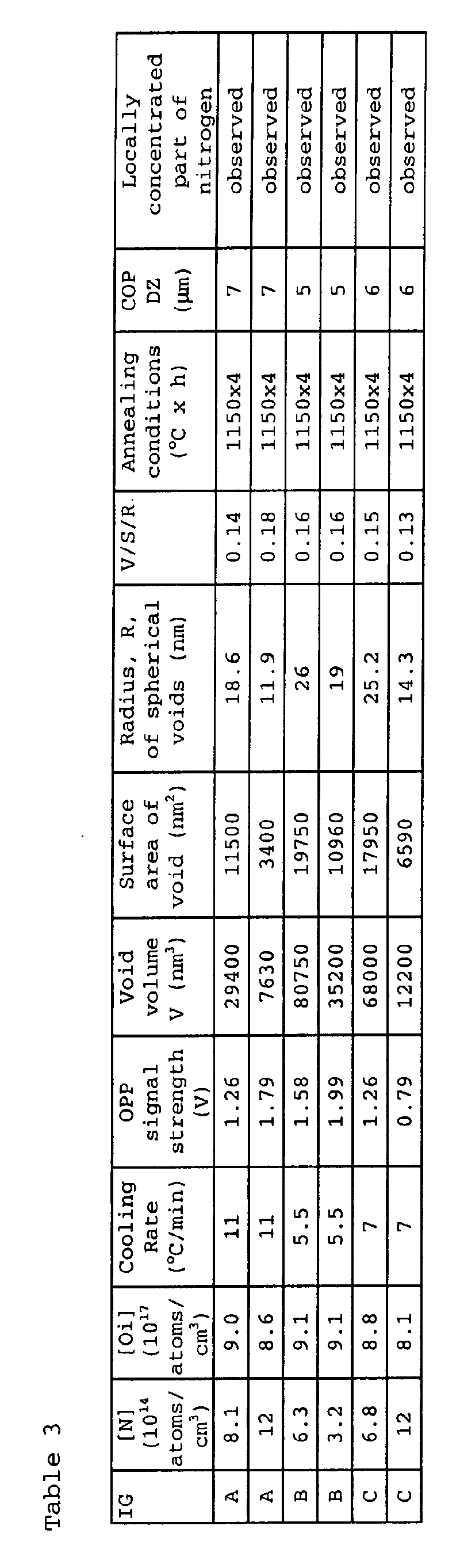
- the working examples possessed such nitrogen concentrations, oxygen concentrations, and cooling rate as falling within the respective ranges contemplated by this invention, they satisfied the relational expression, 0.2 ⁇ V/S/R, indicating the change in shape of voids and, at the same time, attained the depth of a defect-free layer allowing the presence of void type defects (indicated as COP DZ in the table) to greater regions than those attainable heretofore.
- the COP DZ layers showed no discernible sign of oxygen precipitate defects.
- the definition of the COP DZ is that the COP volume density obtained after the repeated washing with the SC-1 liquid mixture be not more than 2 ⁇ 10 5 pieces/cm 3 and the region satisfying the lower limit of 11 MV/cm under application of 100 mA/cm 2 in the evaluation of TZDB be not less than 90 %.
- Comparative Example 1 (Wafer having a diameter of 6 inches)
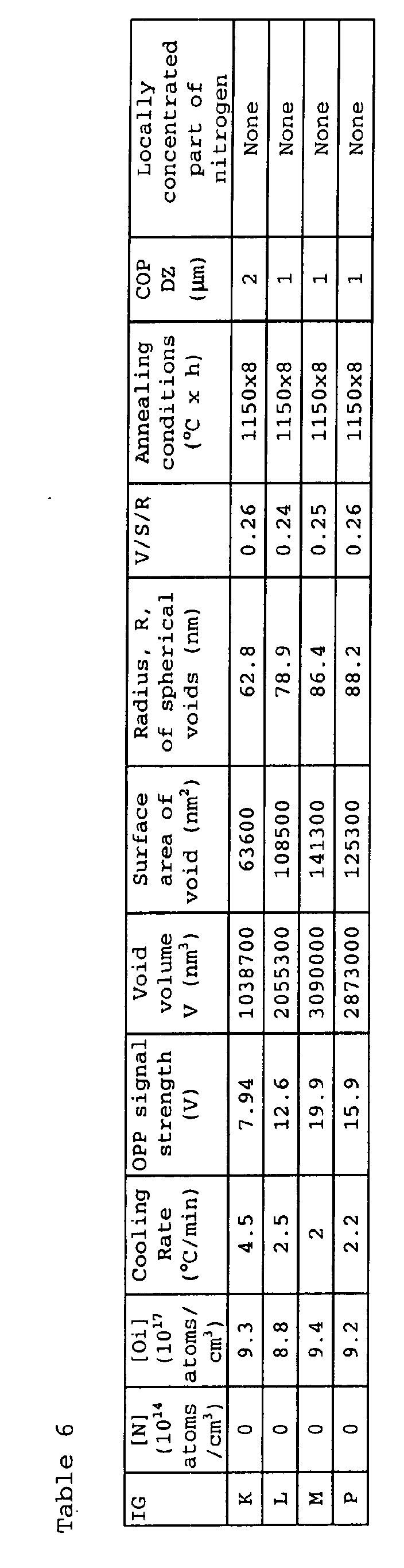
- Silicon semiconductor substrates obtained by using silicon semiconductor substrates not satisfying claim 3 (also claim 1 and claim 2) and still awaiting the heat treatment and heat-treating them under the conditions satisfying claim 7 were examined to confirm the COP DZ. The results are shown in Table 4.
- Example 3 (Wafer having a diameter of 8 inches)
- Examples of silicon semiconductor substrates using wafers awaiting the heat treatment of claim 4 (also satisfying claim 1 and claim 2) and satisfying the conditions of claim 8 (also satisfying claim 5 and claim 6) are indicated as ingots (row of IG) H and I in the following Table 5 and examples of silicon semiconductor substrates satisfying claim 1 are indicated as ingots O.
- the samples of this example possessed such nitrogen concentrations, oxygen concentrations, and cooling rate as falling within the respective ranges contemplated by this invention prior to undergoing the heat treatment defined by this invention, they satisfied the relational expression, 0.2 ⁇ V/S/R, indicating the change in shape of voids according to the invention and, at the same time, attained the depth of a defect-free layer allowing the presence of void type defects (indicated as COP DZ in the table) to greater regions than those attainable heretofore as shown in the data of Table 5 mentioned above. Incidentally the COP DZ layers of the samples showed no discernible sign of oxygen precipitate defects.
- the ingots H and I satisfied the condition for the nitrogen concentration to be in the range between 5 ⁇ 10 14 atoms/cm 3 and 1 ⁇ 10 16 atoms/cm 3 , whereas the ingot O did not satisfy this range but satisfied only the relational expression 0.2 ⁇ V/S/R. This fact justifies an inference that the depth of COP DZ was small when the duration of the heat treatment was insufficient.
- Comparative Example 2 (Wafers having diameters of 8 and 12 inches)
- the ingot M measured 8 inches in diameter and showed a low cooling rate.
- the ingot P measured 12 inches in diameter did not allow easy extinction of voids even when it was heat-treated in the aforementioned non-oxidising atmosphere at 1150 °C for eight hours because it had large void volumes.
- the data suggest that the ease with which the extinction of voids was attained decreased in proportion as the increase of the void volumes and the extinction was in need of the effect of this invention.
- the voids underwent changes of form within the range defined by the relational expression, 0.2 ⁇ V/S/R, and nevertheless allowed no easy extinction of voids by the heat treatment because of excessively large void volumes.
- These results imply that more preferably the nitrogen concentrations ought to be controlled within the range between 5 ⁇ 10 14 atoms/cm 3 and 1 ⁇ 10 16 atoms/cm 3 as demonstrated in Example 3.
- the regions of COP DZ were expanded to greater depths than when the change in form of voids did not satisfy the relational expression, 0.2 ⁇ V/S/R, as demonstrated in Comparative.
- Example 2 described above wafers resulting from heat-treating materials incorporating no nitrogen).
- Example 5 (Wafers measuring 6, 8, and 12 inches in diameter and using a maximum final temperature of 1200 °C)
- Claim 9 and claim 10 recite techniques for producing silicon semiconductor substrates having COP DZ of not less than 5 ⁇ m and less than 12 ⁇ m by using silicon semiconductor substrates satisfying claim 3 and claim 4 and still awaiting the heat treatment and subjecting such substrates to the heat treatment recited in claim 9 and claim 10.
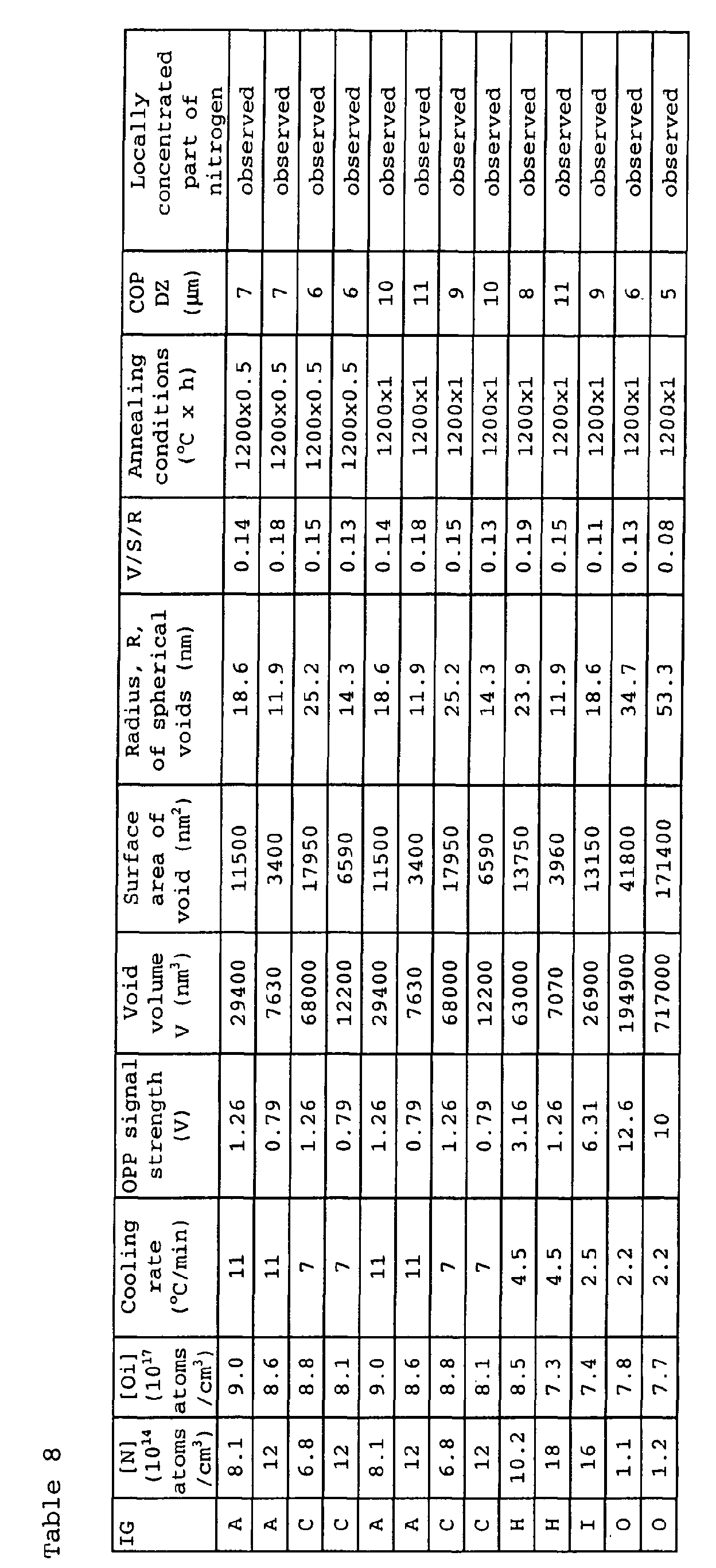
- the depths of COP DZ were invariably not less than 5 ⁇ m and less than 12 ⁇ m.
- the oxygen concentrations consequently found were not more than 6 ⁇ 10 16 atoms/cm 3 .
- the found values of density were not more than 1x10 9 pieces/cm 3 .
- the depths of COP DZ were invariably not less than 5 ⁇ m and less than 12 ⁇ m.
- the oxygen concentrations consequently found were not more than 5 ⁇ 10 16 atoms/cm 3 .
- the found values of density were not more than 1 ⁇ 10 9 pieces/cm 3 .
- Table 8 The results of Table 8 were summarised so as to be easily compared with those of the samples satisfying claim 7 and claim 8.
- the case of performing the heat treatment at a temperature of 1150 °C and the case of performing the heat treatment at a temperature of 1200 °C as in Examples 1 and 2 were compared in terms of the duration of heat treatment.
- the results are shown in Table 9 (indicated in the ratios based on 1150 °C ⁇ 4 hours taken as 1).
- the duration of the heat treatment embraces the duration required in inserting a sample in an oven at 800 °C when the wafer measured 6 inches in diameter and at 700 °C when the wafer measured 8 inches or 12 inches and the duration required in increasing the temperature to 1150 °C and 1200 °C and decreasing the temperature thence.
- COP DZ as used in this specification is defined as the presence of the freeness from the defects at the relevant depth which is announced when the COP volume density attained by the repeated washing is not more than 2 ⁇ 10 5 pieces/cm 3 and the ratio of acceptance of TZDB is not less than 90 %. Naturally, this region shows no discernible sign of oxygen precipitates which are useful for the gettering of impurities.
- the silicon semiconductor substrate contemplated by this invention has only to control the amount of nitrogen to be added, the oxygen concentration, and the cooling rate of the silicon single crystal being pulled while this crystal during the ascent passes through a temperature zone of 1100 °C within specific ranges fit for easy extinction of void type defects by an annealing material to produce a silicon semiconductor showing a satisfactory device yield and enjoying high quality. Further, the reduction in the duration of production can be realised.
Landscapes
- Chemical & Material Sciences (AREA)
- Engineering & Computer Science (AREA)
- Crystallography & Structural Chemistry (AREA)
- Materials Engineering (AREA)
- Metallurgy (AREA)
- Organic Chemistry (AREA)
- Crystals, And After-Treatments Of Crystals (AREA)
Abstract
Description
| Ingot | Nitrogen concentration in melt (atoms/cm3) | Cooling rate (°C/min) | Oxygen concentration (atoms/cm3) | Average SL (mm/min) | Wafer diameter (inches) |
| A (e) | 5x10¹⁷ | 11 | 8.5∼9.5x10¹⁷ | 2.2 | 6 |
| B (e) | 3x10¹⁷ | 5.5 | 8.5∼9.5x10¹⁷ | 1.5 | 6 |
| C (e) | 5x10¹⁷ | 7 | 8.0∼9.0x10¹⁷ | 1.8 | 6 |
| D (c) | 0 | 11 | 8.5∼9.5x10¹⁷ | 2.2 | 6 |
| E (c) | 0 | 7 | 8.5∼9.5x10¹⁷ | 1.8 | 6 |
| F (c) | 1x10¹⁷ | 11 | 8.5∼9.5x10¹⁷ | 2.2 | 6 |
| G (c) | 1x10¹⁷ | 5.5 | 8.5∼9.5x10¹⁷ | 1.5 | 6 |
| H (e) | 1x10¹⁸ | 4.5 | 7.5∼8.5x10¹⁷ | 1.4 | 8 |
| I (e) | 1x10¹⁸ | 2.5 | 7.0∼8.0x10¹⁷ | 1.1 | 8 |
| J (e) | 1x10¹⁸ | 2 | 7.0∼8.0x10¹⁷ | 0.8 | 8 |
| K (c) | 0 | 4.5 | 8.5∼9.5x10¹⁷ | 1.4 | 8 |
| L (c) | 0 | 2.5 | 8.5∼9.5x10¹⁷ | 1.1 | 8 |
| M (c) | 0 | 2 | 8.5∼9.5x10¹⁷ | 0.8 | 8 |
| N (c) | 2x10¹⁷ | 2.5 | 7.0∼8.0x10¹⁷ | 1.1 | 8 |
| O (e) | 1x10¹⁸ | 2.2 | 7.0∼8.0x10¹⁷ | 0.8 | 12 |
| P (c) | 0 | 2.2 | 8.5∼9.5x10¹⁷ | 0.8 | 12 |
| Q (e, c) | 5x10¹⁷ | 1.5 | 8.0∼9.0x10¹⁷ | 0.8 | 6 |
| R (e, c) | 1x10¹⁶ | 1.5 | 8.0∼9.0x10¹⁷ | 0.8 | 6 |




| Diameter of wafer (inch) | Temperature during insertion (°C) | Temperature and duration of heat treatment (°C x h) | Ratio of duration of heat treatment | COP DZ (µm) |
| 6 | 800 | 1150 x 4 | 1 | 6∼7 |
| 6 | 800 | 1200 x 0.5 | 0.68 | 6∼7 |
| 6 | 800 | 1200 x 1 | 0.88 | 9∼11 |
| 8 | 700 | 1150 x 8 | 1.4 | 6 |
| 8 | 700 | 1200 x 1 | 1 | 8∼11 |
| 12 | 700 | 1150 x 8 | 1.4 | 4 |
| 12 | 700 | 1200 x 1 | 1 | 5∼6 |
Claims (10)
- A silicon semiconductor substrate derived from a silicon single crystal grown by the Czochralski method or the magnetic field-applied Czochralski method, characterised by satisfying the relation, 0.2 ≥ V/S/R, providing V denotes the volume of void type defects, S the surface area thereof, and R the radius of spherical defects presumed to have the same volume as the void type defects having the volume of V.
- A silicon semiconductor substrate according to claim 1, which contains nitrogen at a concentration of not less than 1×10¹⁴ atoms/cm3 and not more than 1×10¹⁶ atoms/cm3.
- A silicon semiconductor substrate according to claim 1, wherein the void type defects in the silicon semiconductor substrate having an oxygen concentration of not more than 9.5×10¹⁷ atoms/cm3 and a nitrogen concentration of not less than 5×10¹⁴ atoms/cm3 and not more than 1×10¹⁶ atoms/cm3, when presumed to have spherical volumes, have a radius R satisfying R ≤ 30 nm.
- A silicon semiconductor substrate according to claim 1, wherein the void type defects in the silicon semiconductor substrate having an oxygen concentration of not more than 8.5×10¹⁷ atoms/cm3 and a nitrogen concentration of not less than 5×10¹⁴ atoms/cm3 and not more than 1×10¹⁶ atoms/cm3, when presumed to have spherical volumes, have a radius R satisfying R ≤ 75 nm.
- A method for the production of a silicon semiconductor substrate, characterised by
providing a silicon semiconductor substrate set forth in claim 1 as derived from a silicon single crystal grown by the Czochralski method or the magnetic field-applied Czochralski method using a cooling rate of not less than 1 °C/min while the silicon single crystal being pulled passes through a temperature zone of 1100 °C
and heat-treating the silicon semiconductor substrate in a non-oxidising atmosphere at a temperature of not less than 1150 °C for not less than one hour. - A method for the production of a silicon semiconductor substrate, characterised by
providing a silicon semiconductor substrate set forth in claim 2 as derived from a silicon single crystal grown by the Czochralski method or the magnetic field-applied Czochralski method using molten silicon containing nitrogen at a concentration of not less than 1×10¹⁷ atoms/cm3 and not more than 1.5×10¹⁹ atoms/cm3 and using a cooling rate of not less than 1 °C/min while the silicon single crystal being pulled passes through a temperature zone of 1100 °C
and heat-treating the silicon semiconductor substrate in a non-oxidising atmosphere at a temperature of not less than 1150 °C for not less than one hour. - A method for the production of a silicon semiconductor substrate, characterised by
providing a silicon semiconductor substrate set forth in claim 3 as derived from a silicon single crystal grown by the Czochralski method or the magnetic field-applied Czochralski method using molten silicon containing nitrogen at a concentration of not less than 5×10¹⁷ atoms/cm3 and not more than 1.5×10¹⁹ atoms/cm3 and using a cooling rate of not less than 5 °C/min while the silicon single crystal being pulled passes through a temperature zone of 1100 °C
and heat-treating the silicon semiconductor substrate in a non-oxidising atmosphere at a temperature of not less than 1150 °C for not less than one hour. - A method for the production of a silicon semiconductor substrate, characterised by
providing a silicon semiconductor substrate set forth in claim 4 as derived from a silicon single crystal grown by the Czochralski method or the magnetic field-applied Czochralski method using molten silicon containing nitrogen at a concentration of not less than 1×10¹⁸ atoms/cm3 and not more than 1.5×10¹⁹ atoms/cm3 and using a cooling rate of not less than 1 °C/min and less than 5 °C/min while the silicon single crystal being pulled passes through a temperature zone of 1100 °C
and heat-treating the silicon semiconductor substrate in a non-oxidising atmosphere at a temperature of not less than 1150 °C for not less than one hour. - A method for the production of a silicon semiconductor substrate, characterised by heat-treating a silicon semiconductor substrate set forth in claim 3 in a non-oxidising atmosphere at a temperature of not less than 1200 °C thereby causing the semiconductor substrate to acquire an oxygen concentration of not more than 6×10¹⁶ atoms/cm3 at a depth of 1 µm from the surface at the centre thereof, a locally concentrated part originating in a nitrogen segregation exhibiting a concentration of not less than twice as high as the average signal strength at the centre of the silicon substrate depth in the determination of nitrogen concentration by the method of secondary ion mass analysis (SIMS), a surface defect-free layer of a depth of not less than 5 µm and less than 12 µm from the surface, and an oxygen precipitate density of not less than 1×10⁹ pieces/cm3 at the centre of depth of the central part of the silicon substrate.
- A method for the production of a silicon semiconductor substrate, characterised by heat-treating a silicon semiconductor substrate set forth in claim 4 in a non-oxidising atmosphere at a temperature of not less than 1200 °C thereby causing the semiconductor substrate to acquire an oxygen concentration of not more than 5×10¹⁶ atoms/cm3 at a depth of 1 µm from the surface at the centre thereof, a locally concentrated part originating in a nitrogen segregation exhibiting a concentration of not less than twice as high as the average signal strength at the centre of the silicon substrate depth in the determination of nitrogen concentration by the method of secondary ion mass analysis (SIMS), a surface defect-free layer of a depth of not less than 5 µm and less than 12 µm from the surface, and an oxygen precipitate density of not less than 5×10⁸ pieces/cm3 at the centre of depth of the central part of the silicon substrate.
Applications Claiming Priority (2)
| Application Number | Priority Date | Filing Date | Title |
|---|---|---|---|
| JP2001280460 | 2001-09-14 | ||
| JP2001280460A JP4549589B2 (en) | 2001-09-14 | 2001-09-14 | Silicon semiconductor substrate and manufacturing method thereof |
Publications (3)
| Publication Number | Publication Date |
|---|---|
| EP1293591A2 true EP1293591A2 (en) | 2003-03-19 |
| EP1293591A3 EP1293591A3 (en) | 2003-06-04 |
| EP1293591B1 EP1293591B1 (en) | 2005-11-30 |
Family
ID=19104455
Family Applications (1)
| Application Number | Title | Priority Date | Filing Date |
|---|---|---|---|
| EP02019801A Expired - Lifetime EP1293591B1 (en) | 2001-09-14 | 2002-09-05 | Silicon semiconductor substrate and method for production thereof |
Country Status (7)
| Country | Link |
|---|---|
| US (1) | US6767848B2 (en) |
| EP (1) | EP1293591B1 (en) |
| JP (1) | JP4549589B2 (en) |
| KR (1) | KR100526427B1 (en) |
| CN (1) | CN1194382C (en) |
| DE (1) | DE60207657T2 (en) |
| TW (1) | TWI231548B (en) |
Families Citing this family (11)
| Publication number | Priority date | Publication date | Assignee | Title |
|---|---|---|---|---|
| JP4567251B2 (en) * | 2001-09-14 | 2010-10-20 | シルトロニック・ジャパン株式会社 | Silicon semiconductor substrate and manufacturing method thereof |
| KR100573473B1 (en) * | 2004-05-10 | 2006-04-24 | 주식회사 실트론 | Silicon Wafer and Manufacturing Method Thereof |
| DE102005046726B4 (en) * | 2005-09-29 | 2012-02-02 | Siltronic Ag | Non-polished monocrystalline silicon wafer and process for its production |
| JP5358189B2 (en) * | 2006-01-20 | 2013-12-04 | インフィネオン テクノロジーズ オーストリア アクチエンゲゼルシャフト | Oxygen-containing semiconductor wafer processing method |
| KR100851137B1 (en) * | 2006-10-10 | 2008-08-08 | 현대자동차주식회사 | jig for recognizing a kind of wheel nut and mounting the same |
| US7977216B2 (en) * | 2008-09-29 | 2011-07-12 | Magnachip Semiconductor, Ltd. | Silicon wafer and fabrication method thereof |
| EP2309038B1 (en) * | 2009-10-08 | 2013-01-02 | Siltronic AG | production method of an epitaxial wafer |
| CN103855098B (en) * | 2012-12-04 | 2017-05-17 | 中芯国际集成电路制造(上海)有限公司 | Method for forming storage unit of flash memory |
| US9255343B2 (en) | 2013-03-08 | 2016-02-09 | Ut-Battelle, Llc | Iron-based composition for magnetocaloric effect (MCE) applications and method of making a single crystal |
| CN105297140B (en) * | 2015-09-10 | 2019-10-25 | 上海超硅半导体有限公司 | Silicon wafer and annealing method |
| JP6761917B1 (en) * | 2019-11-29 | 2020-09-30 | Jx金属株式会社 | Method for manufacturing indium phosphide substrate, semiconductor epitaxial wafer, and indium phosphide substrate |
Family Cites Families (29)
| Publication number | Priority date | Publication date | Assignee | Title |
|---|---|---|---|---|
| JP3080501B2 (en) * | 1993-03-01 | 2000-08-28 | 東芝セラミックス株式会社 | Silicon wafer manufacturing method |
| DE19637182A1 (en) * | 1996-09-12 | 1998-03-19 | Wacker Siltronic Halbleitermat | Process for the production of silicon wafers with low defect density |
| US5930762A (en) * | 1996-09-24 | 1999-07-27 | Rco Software Limited | Computer aided risk management in multiple-parameter physical systems |
| JPH1179889A (en) * | 1997-07-09 | 1999-03-23 | Shin Etsu Handotai Co Ltd | Method and apparatus for producing silicon single crystal with few crystal defects and silicon single crystal and silicon wafer produced by this method and apparatus |
| JP3144631B2 (en) * | 1997-08-08 | 2001-03-12 | 住友金属工業株式会社 | Heat treatment method for silicon semiconductor substrate |
| KR100395181B1 (en) * | 1997-08-26 | 2003-08-21 | 미츠비시 스미토모 실리콘 주식회사 | High-quality silicon single crystal and method of producing the same |
| TW429478B (en) * | 1997-08-29 | 2001-04-11 | Toshiba Corp | Semiconductor device and method for manufacturing the same |
| JPH11135511A (en) * | 1997-10-29 | 1999-05-21 | Nippon Steel Corp | Silicon semiconductor substrate and method of manufacturing the same |
| JP3596257B2 (en) * | 1997-11-19 | 2004-12-02 | 三菱住友シリコン株式会社 | Manufacturing method of silicon single crystal wafer |
| US6021397A (en) * | 1997-12-02 | 2000-02-01 | Financial Engines, Inc. | Financial advisory system |
| TW589415B (en) * | 1998-03-09 | 2004-06-01 | Shinetsu Handotai Kk | Method for producing silicon single crystal wafer and silicon single crystal wafer |
| US6078904A (en) * | 1998-03-16 | 2000-06-20 | Saddle Peak Systems | Risk direct asset allocation and risk resolved CAPM for optimally allocating investment assets in an investment portfolio |
| JP4084902B2 (en) * | 1998-05-01 | 2008-04-30 | シルトロニック・ジャパン株式会社 | Silicon semiconductor substrate and manufacturing method thereof |
| US6548886B1 (en) * | 1998-05-01 | 2003-04-15 | Wacker Nsce Corporation | Silicon semiconductor wafer and method for producing the same |
| JPH11349393A (en) * | 1998-06-03 | 1999-12-21 | Shin Etsu Handotai Co Ltd | Silicon single crystal wafer and method for manufacturing silicon single crystal wafer |
| EP1035235A4 (en) * | 1998-08-31 | 2002-05-15 | Shinetsu Handotai Kk | PROCESS FOR PRODUCING SINGLE-CRYSTAL SILICON WAFER AND SINGLE-CRYSTAL SILICON WAFER |
| US6292787B1 (en) * | 1998-09-11 | 2001-09-18 | Financial Engines, Inc. | Enhancing utility and diversifying model risk in a portfolio optimization framework |
| JP3975605B2 (en) * | 1998-11-17 | 2007-09-12 | 信越半導体株式会社 | Silicon single crystal wafer and method for producing silicon single crystal wafer |
| US6219649B1 (en) * | 1999-01-21 | 2001-04-17 | Joel Jameson | Methods and apparatus for allocating resources in the presence of uncertainty |
| JP2000256092A (en) * | 1999-03-04 | 2000-09-19 | Shin Etsu Handotai Co Ltd | Silicon wafer |
| DE60043661D1 (en) * | 1999-08-27 | 2010-02-25 | Komatsu Denshi Kinzoku K K | SILICON SURFACE, METHOD OF MANUFACTURING AND EVALUATION METHOD THEREFOR |
| KR100378184B1 (en) * | 1999-11-13 | 2003-03-29 | 삼성전자주식회사 | Silicon wafer having controlled distribution of defects, process for the preparation of the same and czochralski puller for manufacturing monocrystalline silicon ingot |
| JP3601383B2 (en) * | 1999-11-25 | 2004-12-15 | 信越半導体株式会社 | Epitaxial growth silicon wafer, epitaxial wafer and manufacturing method thereof |
| JP2001220291A (en) * | 2000-02-01 | 2001-08-14 | Komatsu Electronic Metals Co Ltd | Method for manufacturing silicon wafer |
| AU2001265194A1 (en) * | 2000-05-30 | 2001-12-11 | Ittai Korin | Method and system for analyzing performance of an investment portfolio together with associated risk |
| US20020062271A1 (en) * | 2000-10-13 | 2002-05-23 | Peter Breuninger | Method and system for managing portfolio accounts |
| US7536332B2 (en) * | 2001-02-02 | 2009-05-19 | Rhee Thomas A | Real life implementation of modern portfolio theory (MPT) for financial planning and portfolio management |
| US20020198809A1 (en) * | 2001-05-23 | 2002-12-26 | Daley R. Michael | System and method for managing investment accounts for a financial institution which provides investment assistance to individual client investors |
| US20020198811A1 (en) * | 2001-06-12 | 2002-12-26 | Adam Wizon | System and method for monitoring the status of analyses performed on a portfolio of financial instruments |
-
2001
- 2001-09-14 JP JP2001280460A patent/JP4549589B2/en not_active Expired - Lifetime
-
2002
- 2002-09-05 EP EP02019801A patent/EP1293591B1/en not_active Expired - Lifetime
- 2002-09-05 DE DE60207657T patent/DE60207657T2/en not_active Expired - Lifetime
- 2002-09-10 KR KR10-2002-0054571A patent/KR100526427B1/en not_active Expired - Lifetime
- 2002-09-11 US US10/241,180 patent/US6767848B2/en not_active Expired - Lifetime
- 2002-09-12 TW TW091120811A patent/TWI231548B/en not_active IP Right Cessation
- 2002-09-16 CN CNB021431809A patent/CN1194382C/en not_active Expired - Lifetime
Also Published As
| Publication number | Publication date |
|---|---|
| US6767848B2 (en) | 2004-07-27 |
| JP2003086597A (en) | 2003-03-20 |
| EP1293591B1 (en) | 2005-11-30 |
| TWI231548B (en) | 2005-04-21 |
| DE60207657T2 (en) | 2006-06-08 |
| CN1405841A (en) | 2003-03-26 |
| CN1194382C (en) | 2005-03-23 |
| KR100526427B1 (en) | 2005-11-08 |
| EP1293591A3 (en) | 2003-06-04 |
| US20030134520A1 (en) | 2003-07-17 |
| KR20030023509A (en) | 2003-03-19 |
| DE60207657D1 (en) | 2006-01-05 |
| JP4549589B2 (en) | 2010-09-22 |
Similar Documents
| Publication | Publication Date | Title |
|---|---|---|
| KR100369760B1 (en) | Method for Manufacturing a Silicon Wafer | |
| KR100581046B1 (en) | Method of manufacturing silicon single crystal wafer and silicon single crystal wafer | |
| US20020179003A1 (en) | Silicon wafer, silicon epitaxial wafer, anneal wafer and method for producing them | |
| EP0965662B1 (en) | Method for producing low defect silicon single crystal doped with nitrogen | |
| EP1293591B1 (en) | Silicon semiconductor substrate and method for production thereof | |
| EP1391921A1 (en) | METHOD FOR PREPARING NITROGEN−DOPED AND ANNEALED WAFER AND NITROGEN−DOPED AND ANNEALED WAFER | |
| EP1502972B1 (en) | A silicon single crystal wafer, an epitaxial wafer and method for producing silicon single crystal | |
| US6902618B2 (en) | Silicon single crystal wafer having void denuded zone on the surface and diameter of above 300 mm and its production method | |
| US7208043B2 (en) | Silicon semiconductor substrate and preparation thereof | |
| EP1829992B1 (en) | Method for producing single crystal and a method for producing annealed wafer | |
| EP1536044B1 (en) | Method of manufacturing an epitaxial silicon wafer | |
| EP1420440B1 (en) | An epitaxial wafer and a method for producing it | |
| EP1804283B1 (en) | Manufacturing method of annealed wafer | |
| US6599603B1 (en) | Silicon wafer | |
| JP2002016071A (en) | Silicon wafer manufacturing method and silicon wafer manufactured by the method | |
| WO2005053010A1 (en) | Annealed wafer and annealed wafer manufacturing method | |
| EP1127962B1 (en) | Method for manufacturing silicon single crystal, silicon single crystal manufactured by the method, and silicon wafer | |
| Abe et al. | A history and future of silicon crystal growth | |
| Abe | the IC (integrated circuit) invention. Controls of dopants (BР) and light elements (CNO), elimination of heavy metals (Cu, Fe) have been done but a behavior of the point defects has | |
| Abe | Isobe, Annaka, Gunma 379-0134, Japan |
Legal Events
| Date | Code | Title | Description |
|---|---|---|---|
| PUAI | Public reference made under article 153(3) epc to a published international application that has entered the european phase |
Free format text: ORIGINAL CODE: 0009012 |
|
| 17P | Request for examination filed |
Effective date: 20020905 |
|
| AK | Designated contracting states |
Kind code of ref document: A2 Designated state(s): AT BE BG CH CY CZ DE DK EE ES FI FR GB GR IE IT LI LU MC NL PT SE SK TR |
|
| AX | Request for extension of the european patent |
Extension state: AL LT LV MK RO SI |
|
| PUAL | Search report despatched |
Free format text: ORIGINAL CODE: 0009013 |
|
| AK | Designated contracting states |
Designated state(s): AT BE BG CH CY CZ DE DK EE ES FI FR GB GR IE IT LI LU MC NL PT SE SK TR |
|
| AX | Request for extension of the european patent |
Extension state: AL LT LV MK RO SI |
|
| 17Q | First examination report despatched |
Effective date: 20030624 |
|
| AKX | Designation fees paid |
Designated state(s): DE |
|
| RAP1 | Party data changed (applicant data changed or rights of an application transferred) |
Owner name: SILTRONIC AG |
|
| GRAP | Despatch of communication of intention to grant a patent |
Free format text: ORIGINAL CODE: EPIDOSNIGR1 |
|
| GRAS | Grant fee paid |
Free format text: ORIGINAL CODE: EPIDOSNIGR3 |
|
| GRAA | (expected) grant |
Free format text: ORIGINAL CODE: 0009210 |
|
| AK | Designated contracting states |
Kind code of ref document: B1 Designated state(s): DE |
|
| REF | Corresponds to: |
Ref document number: 60207657 Country of ref document: DE Date of ref document: 20060105 Kind code of ref document: P |
|
| PLBE | No opposition filed within time limit |
Free format text: ORIGINAL CODE: 0009261 |
|
| STAA | Information on the status of an ep patent application or granted ep patent |
Free format text: STATUS: NO OPPOSITION FILED WITHIN TIME LIMIT |
|
| 26N | No opposition filed |
Effective date: 20060831 |
|
| PGFP | Annual fee paid to national office [announced via postgrant information from national office to epo] |
Ref country code: DE Payment date: 20210920 Year of fee payment: 20 |
|
| REG | Reference to a national code |
Ref country code: DE Ref legal event code: R071 Ref document number: 60207657 Country of ref document: DE |