EP1291906A1 - Semiconductor device and fabrication method therefor - Google Patents
Semiconductor device and fabrication method therefor Download PDFInfo
- Publication number
- EP1291906A1 EP1291906A1 EP01915802A EP01915802A EP1291906A1 EP 1291906 A1 EP1291906 A1 EP 1291906A1 EP 01915802 A EP01915802 A EP 01915802A EP 01915802 A EP01915802 A EP 01915802A EP 1291906 A1 EP1291906 A1 EP 1291906A1
- Authority
- EP
- European Patent Office
- Prior art keywords
- forming
- wiring
- metal foil
- semiconductor device
- etching
- Prior art date
- Legal status (The legal status is an assumption and is not a legal conclusion. Google has not performed a legal analysis and makes no representation as to the accuracy of the status listed.)
- Granted
Links
Images



Classifications
-
- H—ELECTRICITY
- H10—SEMICONDUCTOR DEVICES; ELECTRIC SOLID-STATE DEVICES NOT OTHERWISE PROVIDED FOR
- H10W—GENERIC PACKAGES, INTERCONNECTIONS, CONNECTORS OR OTHER CONSTRUCTIONAL DETAILS OF DEVICES COVERED BY CLASS H10
- H10W72/00—Interconnections or connectors in packages
- H10W72/071—Connecting or disconnecting
-
- H—ELECTRICITY
- H10—SEMICONDUCTOR DEVICES; ELECTRIC SOLID-STATE DEVICES NOT OTHERWISE PROVIDED FOR
- H10W—GENERIC PACKAGES, INTERCONNECTIONS, CONNECTORS OR OTHER CONSTRUCTIONAL DETAILS OF DEVICES COVERED BY CLASS H10
- H10W72/00—Interconnections or connectors in packages
- H10W72/01—Manufacture or treatment
- H10W72/012—Manufacture or treatment of bump connectors, dummy bumps or thermal bumps
-
- H—ELECTRICITY
- H10—SEMICONDUCTOR DEVICES; ELECTRIC SOLID-STATE DEVICES NOT OTHERWISE PROVIDED FOR
- H10W—GENERIC PACKAGES, INTERCONNECTIONS, CONNECTORS OR OTHER CONSTRUCTIONAL DETAILS OF DEVICES COVERED BY CLASS H10
- H10W72/00—Interconnections or connectors in packages
- H10W72/01—Manufacture or treatment
- H10W72/0198—Manufacture or treatment batch processes
-
- H—ELECTRICITY
- H10—SEMICONDUCTOR DEVICES; ELECTRIC SOLID-STATE DEVICES NOT OTHERWISE PROVIDED FOR
- H10W—GENERIC PACKAGES, INTERCONNECTIONS, CONNECTORS OR OTHER CONSTRUCTIONAL DETAILS OF DEVICES COVERED BY CLASS H10
- H10W74/00—Encapsulations, e.g. protective coatings
- H10W74/10—Encapsulations, e.g. protective coatings characterised by their shape or disposition
- H10W74/111—Encapsulations, e.g. protective coatings characterised by their shape or disposition the semiconductor body being completely enclosed
- H10W74/129—Encapsulations, e.g. protective coatings characterised by their shape or disposition the semiconductor body being completely enclosed forming a chip-scale package [CSP]
-
- H—ELECTRICITY
- H10—SEMICONDUCTOR DEVICES; ELECTRIC SOLID-STATE DEVICES NOT OTHERWISE PROVIDED FOR
- H10W—GENERIC PACKAGES, INTERCONNECTIONS, CONNECTORS OR OTHER CONSTRUCTIONAL DETAILS OF DEVICES COVERED BY CLASS H10
- H10W70/00—Package substrates; Interposers; Redistribution layers [RDL]
- H10W70/01—Manufacture or treatment
- H10W70/05—Manufacture or treatment of insulating or insulated package substrates, or of interposers, or of redistribution layers
-
- H—ELECTRICITY
- H10—SEMICONDUCTOR DEVICES; ELECTRIC SOLID-STATE DEVICES NOT OTHERWISE PROVIDED FOR
- H10W—GENERIC PACKAGES, INTERCONNECTIONS, CONNECTORS OR OTHER CONSTRUCTIONAL DETAILS OF DEVICES COVERED BY CLASS H10
- H10W70/00—Package substrates; Interposers; Redistribution layers [RDL]
- H10W70/60—Insulating or insulated package substrates; Interposers; Redistribution layers
- H10W70/62—Insulating or insulated package substrates; Interposers; Redistribution layers characterised by their interconnections
- H10W70/65—Shapes or dispositions of interconnections
- H10W70/654—Top-view layouts
- H10W70/656—Fan-in layouts
-
- H—ELECTRICITY
- H10—SEMICONDUCTOR DEVICES; ELECTRIC SOLID-STATE DEVICES NOT OTHERWISE PROVIDED FOR
- H10W—GENERIC PACKAGES, INTERCONNECTIONS, CONNECTORS OR OTHER CONSTRUCTIONAL DETAILS OF DEVICES COVERED BY CLASS H10
- H10W72/00—Interconnections or connectors in packages
- H10W72/01—Manufacture or treatment
- H10W72/012—Manufacture or treatment of bump connectors, dummy bumps or thermal bumps
- H10W72/01231—Manufacture or treatment of bump connectors, dummy bumps or thermal bumps using blanket deposition
- H10W72/01236—Manufacture or treatment of bump connectors, dummy bumps or thermal bumps using blanket deposition in solid form, e.g. by using a powder or by laminating a foil
-
- H—ELECTRICITY
- H10—SEMICONDUCTOR DEVICES; ELECTRIC SOLID-STATE DEVICES NOT OTHERWISE PROVIDED FOR
- H10W—GENERIC PACKAGES, INTERCONNECTIONS, CONNECTORS OR OTHER CONSTRUCTIONAL DETAILS OF DEVICES COVERED BY CLASS H10
- H10W72/00—Interconnections or connectors in packages
- H10W72/01—Manufacture or treatment
- H10W72/012—Manufacture or treatment of bump connectors, dummy bumps or thermal bumps
- H10W72/01251—Changing the shapes of bumps
- H10W72/01253—Changing the shapes of bumps by etching
-
- H—ELECTRICITY
- H10—SEMICONDUCTOR DEVICES; ELECTRIC SOLID-STATE DEVICES NOT OTHERWISE PROVIDED FOR
- H10W—GENERIC PACKAGES, INTERCONNECTIONS, CONNECTORS OR OTHER CONSTRUCTIONAL DETAILS OF DEVICES COVERED BY CLASS H10
- H10W72/00—Interconnections or connectors in packages
- H10W72/01—Manufacture or treatment
- H10W72/013—Manufacture or treatment of die-attach connectors
- H10W72/01331—Manufacture or treatment of die-attach connectors using blanket deposition
-
- H—ELECTRICITY
- H10—SEMICONDUCTOR DEVICES; ELECTRIC SOLID-STATE DEVICES NOT OTHERWISE PROVIDED FOR
- H10W—GENERIC PACKAGES, INTERCONNECTIONS, CONNECTORS OR OTHER CONSTRUCTIONAL DETAILS OF DEVICES COVERED BY CLASS H10
- H10W72/00—Interconnections or connectors in packages
- H10W72/01—Manufacture or treatment
- H10W72/019—Manufacture or treatment of bond pads
- H10W72/01931—Manufacture or treatment of bond pads using blanket deposition
- H10W72/01936—Manufacture or treatment of bond pads using blanket deposition in solid form, e.g. by using a powder or by laminating a foil
-
- H—ELECTRICITY
- H10—SEMICONDUCTOR DEVICES; ELECTRIC SOLID-STATE DEVICES NOT OTHERWISE PROVIDED FOR
- H10W—GENERIC PACKAGES, INTERCONNECTIONS, CONNECTORS OR OTHER CONSTRUCTIONAL DETAILS OF DEVICES COVERED BY CLASS H10
- H10W72/00—Interconnections or connectors in packages
- H10W72/01—Manufacture or treatment
- H10W72/019—Manufacture or treatment of bond pads
- H10W72/01951—Changing the shapes of bond pads
-
- H—ELECTRICITY
- H10—SEMICONDUCTOR DEVICES; ELECTRIC SOLID-STATE DEVICES NOT OTHERWISE PROVIDED FOR
- H10W—GENERIC PACKAGES, INTERCONNECTIONS, CONNECTORS OR OTHER CONSTRUCTIONAL DETAILS OF DEVICES COVERED BY CLASS H10
- H10W72/00—Interconnections or connectors in packages
- H10W72/01—Manufacture or treatment
- H10W72/019—Manufacture or treatment of bond pads
- H10W72/01951—Changing the shapes of bond pads
- H10W72/01953—Changing the shapes of bond pads by etching
-
- H—ELECTRICITY
- H10—SEMICONDUCTOR DEVICES; ELECTRIC SOLID-STATE DEVICES NOT OTHERWISE PROVIDED FOR
- H10W—GENERIC PACKAGES, INTERCONNECTIONS, CONNECTORS OR OTHER CONSTRUCTIONAL DETAILS OF DEVICES COVERED BY CLASS H10
- H10W72/00—Interconnections or connectors in packages
- H10W72/071—Connecting or disconnecting
- H10W72/072—Connecting or disconnecting of bump connectors
- H10W72/07251—Connecting or disconnecting of bump connectors characterised by changes in properties of the bump connectors during connecting
-
- H—ELECTRICITY
- H10—SEMICONDUCTOR DEVICES; ELECTRIC SOLID-STATE DEVICES NOT OTHERWISE PROVIDED FOR
- H10W—GENERIC PACKAGES, INTERCONNECTIONS, CONNECTORS OR OTHER CONSTRUCTIONAL DETAILS OF DEVICES COVERED BY CLASS H10
- H10W72/00—Interconnections or connectors in packages
- H10W72/20—Bump connectors, e.g. solder bumps or copper pillars; Dummy bumps; Thermal bumps
-
- H—ELECTRICITY
- H10—SEMICONDUCTOR DEVICES; ELECTRIC SOLID-STATE DEVICES NOT OTHERWISE PROVIDED FOR
- H10W—GENERIC PACKAGES, INTERCONNECTIONS, CONNECTORS OR OTHER CONSTRUCTIONAL DETAILS OF DEVICES COVERED BY CLASS H10
- H10W72/00—Interconnections or connectors in packages
- H10W72/20—Bump connectors, e.g. solder bumps or copper pillars; Dummy bumps; Thermal bumps
- H10W72/241—Dispositions, e.g. layouts
- H10W72/244—Dispositions, e.g. layouts relative to underlying supporting features, e.g. bond pads, RDLs or vias
-
- H—ELECTRICITY
- H10—SEMICONDUCTOR DEVICES; ELECTRIC SOLID-STATE DEVICES NOT OTHERWISE PROVIDED FOR
- H10W—GENERIC PACKAGES, INTERCONNECTIONS, CONNECTORS OR OTHER CONSTRUCTIONAL DETAILS OF DEVICES COVERED BY CLASS H10
- H10W72/00—Interconnections or connectors in packages
- H10W72/20—Bump connectors, e.g. solder bumps or copper pillars; Dummy bumps; Thermal bumps
- H10W72/251—Materials
-
- H—ELECTRICITY
- H10—SEMICONDUCTOR DEVICES; ELECTRIC SOLID-STATE DEVICES NOT OTHERWISE PROVIDED FOR
- H10W—GENERIC PACKAGES, INTERCONNECTIONS, CONNECTORS OR OTHER CONSTRUCTIONAL DETAILS OF DEVICES COVERED BY CLASS H10
- H10W72/00—Interconnections or connectors in packages
- H10W72/20—Bump connectors, e.g. solder bumps or copper pillars; Dummy bumps; Thermal bumps
- H10W72/251—Materials
- H10W72/252—Materials comprising solid metals or solid metalloids, e.g. PbSn, Ag or Cu
-
- H—ELECTRICITY
- H10—SEMICONDUCTOR DEVICES; ELECTRIC SOLID-STATE DEVICES NOT OTHERWISE PROVIDED FOR
- H10W—GENERIC PACKAGES, INTERCONNECTIONS, CONNECTORS OR OTHER CONSTRUCTIONAL DETAILS OF DEVICES COVERED BY CLASS H10
- H10W72/00—Interconnections or connectors in packages
- H10W72/20—Bump connectors, e.g. solder bumps or copper pillars; Dummy bumps; Thermal bumps
- H10W72/29—Bond pads specially adapted therefor
-
- H—ELECTRICITY
- H10—SEMICONDUCTOR DEVICES; ELECTRIC SOLID-STATE DEVICES NOT OTHERWISE PROVIDED FOR
- H10W—GENERIC PACKAGES, INTERCONNECTIONS, CONNECTORS OR OTHER CONSTRUCTIONAL DETAILS OF DEVICES COVERED BY CLASS H10
- H10W72/00—Interconnections or connectors in packages
- H10W72/90—Bond pads, in general
- H10W72/921—Structures or relative sizes of bond pads
- H10W72/922—Bond pads being integral with underlying chip-level interconnections
-
- H—ELECTRICITY
- H10—SEMICONDUCTOR DEVICES; ELECTRIC SOLID-STATE DEVICES NOT OTHERWISE PROVIDED FOR
- H10W—GENERIC PACKAGES, INTERCONNECTIONS, CONNECTORS OR OTHER CONSTRUCTIONAL DETAILS OF DEVICES COVERED BY CLASS H10
- H10W72/00—Interconnections or connectors in packages
- H10W72/90—Bond pads, in general
- H10W72/921—Structures or relative sizes of bond pads
- H10W72/922—Bond pads being integral with underlying chip-level interconnections
- H10W72/9223—Bond pads being integral with underlying chip-level interconnections with redistribution layers [RDL]
-
- H—ELECTRICITY
- H10—SEMICONDUCTOR DEVICES; ELECTRIC SOLID-STATE DEVICES NOT OTHERWISE PROVIDED FOR
- H10W—GENERIC PACKAGES, INTERCONNECTIONS, CONNECTORS OR OTHER CONSTRUCTIONAL DETAILS OF DEVICES COVERED BY CLASS H10
- H10W72/00—Interconnections or connectors in packages
- H10W72/90—Bond pads, in general
- H10W72/921—Structures or relative sizes of bond pads
- H10W72/923—Bond pads having multiple stacked layers
-
- H—ELECTRICITY
- H10—SEMICONDUCTOR DEVICES; ELECTRIC SOLID-STATE DEVICES NOT OTHERWISE PROVIDED FOR
- H10W—GENERIC PACKAGES, INTERCONNECTIONS, CONNECTORS OR OTHER CONSTRUCTIONAL DETAILS OF DEVICES COVERED BY CLASS H10
- H10W72/00—Interconnections or connectors in packages
- H10W72/90—Bond pads, in general
- H10W72/941—Dispositions of bond pads
- H10W72/942—Dispositions of bond pads relative to underlying supporting features, e.g. bond pads, RDLs or vias
-
- H—ELECTRICITY
- H10—SEMICONDUCTOR DEVICES; ELECTRIC SOLID-STATE DEVICES NOT OTHERWISE PROVIDED FOR
- H10W—GENERIC PACKAGES, INTERCONNECTIONS, CONNECTORS OR OTHER CONSTRUCTIONAL DETAILS OF DEVICES COVERED BY CLASS H10
- H10W72/00—Interconnections or connectors in packages
- H10W72/90—Bond pads, in general
- H10W72/951—Materials of bond pads
- H10W72/952—Materials of bond pads comprising metals or metalloids, e.g. PbSn, Ag or Cu
Definitions
- This invention concerns a chip-size semiconductor device formed with conductor wirings for re-arranging electrodes on an IC chip and it, particularly, relates to a fabrication method capable of collective processing at the wafers.
- JP-A-11-121507 proposes a method of packaging in a state of wafer and fabricating a chip-size package.
- bumps for connecting an IC package with the outside are formed at electrode positions in IC.
- the pitch for arranging electrodes of the chip has been narrowed more and more and it is necessary to re-arrange the electrodes on the IC chip to expand the electrode pitch for facilitating subsequent mounting.
- This invention intends to solve the foregoing problems in the prior art and provide a method of fabricating a chip-size package in which the electrode pitch is extended by forming conductor wirings on the side of the electrode forming surface of a semiconductor element efficiently and at a reduced cost and, particularly, to provide a method capable of forming wirings and bumps easily.
- the present inventors have found that the foregoing object can be solved by laminating a wiring-forming metal foil on the side of forming electrodes of a semiconductor wafer formed at the surface thereof with circuit elements by using a bonding technique between a metal foil and ceramics previously filed by the present inventors (refer to International Publication No. WO99/58470), and then etching the metal foil to form wirings and dividing the same into individual elements.
- bumps can be formed by laminating a wiring-forming multi-layered metal foil to a semiconductor wafer formed at the surface thereof with circuit elements on the side of the electrode forming surface and by merely etching the wirings having bumps thereon.
- this invention described in claim 1 provides a semiconductor device comprising a semiconductor element and conductor wirings on the semiconductor element formed by etching a wiring-forming metal foil (hereinafter referred to as a first embodiment of this invention).
- the wiring-forming metal foil is copper.
- the thickness of the wiring-forming metal foil is preferably 1 to 100 ⁇ m.
- the semiconductor device of the first embodiment according to this invention described above is obtained by a step of laminating a wiring-forming metal foil to a semiconductor wafer formed at the surface thereof with circuit elements on the electrode forming surface side, a step of forming a resist wiring pattern on the metal foil, a step of etching the metal foil and a step of dividing into individual elements as in the invention described in claim 4.
- the wiring-forming metal foil is copper.
- the thickness of the wiring-forming metal foil is 1 to 100 ⁇ m.
- the semiconductor wafer formed at the surface thereof with circuit elements is a semiconductor wafer formed at the surface thereof with a metal thin film.
- the invention described in claim 8 provides a semiconductor device comprising a semiconductor element, conductor wirings formed on the semiconductor element formed by etching a wiring-forming metal foil and solder bumps (hereinafter referred to as a second embodiment of this invention).
- the wiring-forming metal foil is copper.
- the thickness of the wiring-forming metal foil is 1 to 100 ⁇ m.
- the semiconductor device is obtained by a step of laminating a wiring-forming metal foil to the semiconductor wafer formed at the surface thereof with circuit elements on the electrode forming surface side, a step of forming a resist wiring pattern on the metal foil, a step of etching the metal foil, a step of forming solder bumps and a step of dividing into individual elements.
- the wiring-forming metal foil is copper.
- the thickness of the wiring-forming metal foil is 1 to 100 ⁇ m.
- the semiconductor wafer formed at the surface thereof with circuit elements is a semiconductor wafer formed at the surface thereof with a metal thin film.
- the invention described in claim 15 provides a semiconductor device comprising a semiconductor element and a conductor wiring having bumps on the semiconductor element (hereinafter referred to as a third embodiment of this invention).
- the wiring-forming multi-layered metal foil is a metal laminate comprising three layers of bump-forming copper or solder foil/etching stopper layer nickel/wiring-forming copper foil and, further, it is preferred the thickness of the bump forming copper or solder foil is from 10 to 100 ⁇ m.
- the etching stopper layer nickel is preferably nickel plating of 0.5 to 3 ⁇ m thickness or nickel foil clad of 1 to 10 ⁇ m thickness.
- the thickness of the wiring-forming copper foil is 1 to 100 ⁇ m.
- the semiconductor device of the third embodiment according to this invention as described above can be fabricated by a method of fabricating a semiconductor device including a step of laminating a wiring-forming multi-layer metal foil to a semiconductor wafer formed at the surface thereof with circuit elements on the electrode forming surface side, a step of forming a bump-forming resist wiring pattern on the multi-layered metal foil, a step of selectively etching the metal foil, a step of removing the etching stopper layer, a step of forming a wiring-forming resist wiring pattern and a step of forming wirings by etching, and a step of dividing into individual elements.
- the wiring-forming multi-layered metal foil is a metal laminate comprising three layers of a bump forming copper or solder foil/etching stopper layer nickel/wiring forming copper foil. Further, it is preferred that the thickness of the bump-forming copper or soldering foil is 10 to 100 ⁇ m. Further, the etching stopper layer nickel is preferably nickel plating of 0.5 to 3 ⁇ m thickness or nickel foil clad of 1 to 10 ⁇ m thickness. Further, it is preferred that the thickness of the wiring-forming copper foil is 1 to 100 ⁇ m.
- the semiconductor wafer formed at the surface thereof with circuit elements is preferably a semiconductor wafer formed at the surface thereof with a thin metal film.
- the semiconductor device comprises a semiconductor element, a conductor wiring having bumps on the semiconductor element formed by etching a wiring-forming multi-layered metal foil, an insulative resin and solder bumps.
- the method of fabricating the semiconductor device includes a step of laminating a wiring-forming multi-layered metal foil to the semiconductor wafer formed at the surface thereof with circuit elements on the electrode forming surface side, a step of forming a bump-forming resist wiring pattern on the multi-layered metal foil, a step of selectively etching the metal foil, a step of removing the etching stopper layer, a step of forming wiring-forming resist wiring pattern, and a step of forming wirings by etching, a step of coating an insulative resin and polishing the surface thereof, a step of forming solder bumps and a step of dividing into individual elements.
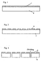
- Fig. 1 is a view showing an example of a circuit forming step for a first embodiment and a second embodiment according to this invention (step of laminating a wiring copper foil on a semiconductor wafer).
- Fig. 2 is a view showing an example of a circuit forming step in a first embodiment and a second embodiment according to this invention (step of forming conductor wirings on the wiring copper foil).
- Fig. 3 is a view showing an example of a circuit forming step in the first embodiment according to this invention (step of cutting into individual elements).
- Fig. 4 is a view showing an example of a circuit forming step in the first embodiment according to this invention (element after cutting).
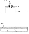
- FIG. 5 is a view showing an example of a circuit forming step in the second embodiment according to this invention (step of forming solder bumps on wiring copper foil).
- Fig. 6 is a view showing an example of a circuit forming step in the second embodiment according to this invention (step of cutting into individual elements).
- Fig. 7 is a view showing an example of a circuit forming step in the second embodiment according to this invention (element after cutting).
- Fig. 8 is a view showing an example of a circuit forming step in a third embodiment according to this invention (step of laminating a wiring copper foil on a semiconductor wafer).
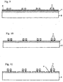
- Fig. 9 is a view showing an example of a circuit forming step in the third embodiment according to this invention (forming bumps).
- FIG. 10 is a view showing an example of a circuit forming step in the. third embodiment according to this invention (selective etching of etching stopper layer nickel).
- Fig. 11 is a view showing an example of a circuit forming step in the third embodiment according to this invention (selective etching of wiring-forming copper foil).
- Fig. 12 is a view showing an example of a circuit forming step in the third embodiment according to this invention (step of cutting into individual elements) .
- Fig. 13 is a view showing an example of a circuit forming step in the third embodiment according to this invention (element after cutting).
- Fig. 14 is a view showing a step of coating an insulative resin and surface polishing in a fourth embodiment according to this invention.
- Fig. 14 is a view showing a step of coating an insulative resin and surface polishing in a fourth embodiment according to this invention.
- Fig. 15 is a view showing a step of forming solder bumps in the fourth embodiment according to this invention.
- Fig. 16 is a view showing a step of cutting into individual elements in the fourth embodiment according to this invention.
- Fig. 17 is a view showing an element after cutting in the fourth embodiment according to this invention.
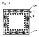
- Fig. 18 is a front elevational view of an element after cutting in the first, second, third or fourth embodiment according to this invention.
- the first embodiment according to this invention concerns a semiconductor device comprising a semiconductor wafer formed at the surface thereof with circuit elements, and conductor wirings on the semiconductor element formed by etching a wiring-forming metal foil.
- a semiconductor wafer or the like used ordinarily can be used and, as the wiring-forming metal foil, a foil preferably formed of copper with a thickness of 1 to 100 ⁇ m can be used.
- the conductor wirings can be formed appropriately into a desired shape.
- the semiconductor device in the first embodiment according to this invention can be fabricated by a method of fabricating a semiconductor device including a step of laminating a wiring-forming metal foil to a semiconductor wafer formed at the surface thereof with circuit elements on the electrode-forming surface side, a step of forming a resist wiring pattern on the metal foil, a step of etching the metal foil and a step of dividing into individual elements.
- the substrate those used ordinarily such as a semiconductor wafer formed at the surface thereof with circuit elements can be used.
- the wiring-forming metal foil a foil preferably formed of copper and of 1 to 100 ⁇ m thickness can be used as described above.
- a thin metal film can be provided on the semiconductor wafer formed at the surface thereof with circuit elements by using a sputtering method, a vapor deposition method or the like after surface cleaning. This can facilitate lamination of the metal foil on the semiconductor wafer.
- the metal forming the thin film Cr, Mo, W or the like is used as a barrier metal in a case where the chip electrode of the semiconductor is Al, but the subsequent removal by etching is difficult. Then, with a view point for the ease of etching elimination, use of nickel is preferred.
- Lamination of the wiring-forming metal foil to the semiconductor wafer can be conducted by using the technique described in International Publication No. WO99/58470 previously filed by the present inventors (Fig. 1).
- a resist is coated on the wiring forming metal foil and then exposure and development are conducted to form a resist wiring pattern.
- the resist wiring pattern is formed preferably such that it can be easily divided subsequently into individual elements and it can adopt, for example, a method of not coating the resist to portions for the division.
- a series of procedures such as resist coating, exposure and development can be conducted based on the ordinary method.
- the wiring-forming metal foil is etched.
- the metal foil is copper
- a commercially available alkali type copper etching solution can be used as the etching solution.
- the second embodiment of this invention concerns a semiconductor device comprising a semiconductor element, conductor wirings on the semiconductor element formed by etching a wire-forming metal foil and solder bumps.
- the semiconductor, the wiring-forming metal foil and the conductor wirings are identical with those described for the first embodiment of this invention.
- the semiconductor device described above can be fabricated by a method of fabricating a semiconductor device including a step of laminating a wiring-forming metal foil to a semiconductor wafer formed at the surface thereof with circuit elements on the electrode forming surface side, a step of forming a resist wiring pattern on the metal foil, a step of etching the metal foil, a step of forming solder bumps and a step of dividing into individual elements.
- a semiconductor wafer formed at the surface thereof with circuit elements can be used usually and, depending on the case, a thin metal film can be provided after surface cleaning of the semiconductor wafer or the like. Further, lamination of the wiring-forming metal foil to the semiconductor wafer can be conducted in the same manner as in the first embodiment of this invention, by using the technique described in International Publication No. WO99/58470 previously filed by the present inventors (Fig. 1).
- a resist is coated on the wiring-forming metal foil and then exposure and development are conducted to form a resist wiring pattern and, successively, the wiring-forming metal foil is etched and then the resist is removed to form wirings (Fig. 2).
- the resist wiring pattern is preferably applied so as to be divided easily into individual elements subsequently like the first embodiment.
- solder bumps are successively formed (Fig. 5).
- the solver bumps are formed at the positions for re-arranging electrodes.
- the third embodiment of this invention concerns a semiconductor device comprising a semiconductor element, and conductor wirings having bumps on the semiconductor element formed by etching the wiring-forming multi-layered metal foil.
- the semiconductor device, the wiring-forming metal foil and the conductor wirings are identical with those described for the first embodiment and the second embodiment of this invention.
- the thickness of the conductor wirings is 1 to 100 ⁇ m as described above, and for the etching stopper layer, nickel plating of 0.5 to 3 ⁇ m thickness, preferably, 1 to 2 ⁇ m thickness or nickel foil clad of 1 to 10 ⁇ m thickness, preferably, 2 to 5 ⁇ m thickness can be used.
- the thickness of the bump is 10 to 100 ⁇ m, preferably, 10 to 50 ⁇ m.
- the semiconductor device according to the third embodiment of this invention described above can be fabricated by a method of fabricating a semiconductor device including a step of laminating a wiring-forming multi-layered metal foil to a semiconductor formed at the surface thereof with circuit elements on the electrode forming surface side, a step of forming a bump-forming resist wiring pattern on the multi-layered metal foil, a step of selectively etching the metal foil, a step of removing the etching stopper layer, a step of forming a wiring-forming resist wiring pattern and a step of forming wirings by etching, and a step of dividing into individual elements.
- a wiring-forming metal laminate is laminated to the semiconductor wafer formed at the surface thereof with circuit elements on the electrode forming surface side (Fig. 8).
- a metal laminate comprising, for example, a bump-forming copper or solder foil (10 to 100 ⁇ m thickness)/etching stopper layer nickel (0.5 to 3 ⁇ m thickness in a case of plating and 1 to 10 ⁇ m thickness in a case of foil)/wiring copper foil (1 to 100 ⁇ m).
- Lamination can be conducted in the same manner as described for the portion of the first embodiment and the second embodiment of this invention.
- resist is coated on the metal laminate and then exposure and development are conducted to form a bump-forming resist pattern.
- the bump forming layer in the metal laminate is selectively etched (Fig. 9).
- etching is conducted by using a selective copper etching solution such a commercially available alkali type copper etching solution to form bumps.
- the etching stopper layer is removed.
- a commercially available nickel removing solution for example, N-950, manufactured by Mertex Co.
- Fig. 10 a commercially available nickel removing solution (for example, N-950, manufactured by Mertex Co.) can be used (Fig. 10).
- a wiring-forming resist wiring pattern is formed.
- the resist wiring pattern is preferably applied so as to indicate the boundary between each of element regions corresponding to the division into individual element regions to be described later, which is identical with that for the first embodiment and the second embodiment of this invention.
- the wiring layer is etched.
- the wiring layer is copper
- a commercially available alkali type copper etching solution or the like can be used.
- the resist is removed (Fig. 11).
- a semiconductor wafer 1 formed at the surface thereof with circuit elements and a wiring-forming copper foil (15 ⁇ m thickness) 2 laminated by the method disclosed in International Publication WO99/58470 were used as a substrate (Fig. 1).
- a thin metal film (nickel) was provided on the semiconductor wafer by using, for example, a sputtering method or a vapor deposition method.
- a chip-size package in which an electrode pitch is expanded by forming conductor wirings to a semiconductor on the electrode forming surface side can be fabricated efficiently and at a reduced cost. Particularly, wirings and bumps can be formed easily.
- the semiconductor device and the wiring forming method according to this invention are useful in the field of semiconductors.
Landscapes
- Internal Circuitry In Semiconductor Integrated Circuit Devices (AREA)
- Wire Bonding (AREA)
- Lead Frames For Integrated Circuits (AREA)
Abstract
Description
Claims (27)
- A semiconductor device comprising a semiconductor element and conductor wirings on the semiconductor element formed by etching a wiring-forming metal foil.
- A semiconductor device as defined in claim 1, wherein the wiring-forming metal foil comprises copper.
- A semiconductor device as defined in claim 1 or 2, wherein the wiring-forming metal foil has a thickness of 1 to 100 µm.
- A method of fabricating a semiconductor device including a step of laminating a wiring-forming metal foil to a semiconductor wafer formed at the surface thereof with circuit elements on the electrode forming surface side, a step of photo-etching the metal foil to form a resist wiring pattern, a step of etching the metal foil and a step of dividing into individual elements.
- A method of fabricating a semiconductor device as defined in claim 4, wherein the wiring-forming metal foil comprises copper.
- A method of fabricating a semiconductor device as defined in claim 4 or 5, wherein the wiring-forming metal foil has a thickness of 1 to 100 µm.
- A method of fabricating a semiconductor device as defined in any one of claims 4 to 6 in which the semiconductor wafer formed at the surface thereof with the circuit element is a semiconductor wafer formed at the surface thereof with a thin metal film.
- A semiconductor device comprising a semiconductor element, conductor wirings on the semiconductor element formed by etching a wiring-forming metal foil, and solder bumps.
- A semiconductor device as defined in claim 8, wherein the wiring-forming metal foil comprises copper.
- A semiconductor device as defined in claim 8 or 9, wherein the wiring-forming metal foil has a thickness of 1 to 100 µm.
- A method of fabricating a semiconductor device including a step of laminating a wiring-forming metal foil to a semiconductor wafer formed at the surface thereof with circuit elements on the electrode forming surface side, a step of forming a resist wiring pattern on the metal, a step of etching the metal foil, a step of forming solder bumps and a step of dividing into individual elements.
- A method of fabricating a semiconductor device as defined in claim 11, wherein the wiring-forming metal foil comprises copper.
- A method of fabricating a semiconductor device as defined in claim 11 or 12, wherein the wiring-forming metal foil has a thickness of 1 to 100 µm.
- A method of fabricating a semiconductor device as defined in any one of claims 11 to 13 in which the semiconductor wafer formed at the surface thereof with circuit elements is a semiconductor wafer formed at the surface thereof with a thin metal film.
- A semiconductor device comprising a semiconductor element and bumps on the semiconductor element formed by etching a wiring-forming multi-layered metal foil.
- A semiconductor device as defined in claim 15, wherein the wiring-forming multi-layered metal foil comprises three layers of bump-forming copper or solder foil/etching stopper layer nickel/wiring-forming copper foil.
- A semiconductor device as defined in claim 15 or 16, wherein the thickness of the bump-forming copper or the solder foil is 10 to 100 µm.
- A semiconductor device as defined in any of claims 15. to 17, wherein the etching stopper layer nickel is nickel plating of 0.5 to 3 µm thickness or nickel foil clad of 1 to 10 µm thickness.
- A semiconductor device as defined in any one'of claims 15 to 18 in which the thickness of the wiring-forming copper foil is 1 to 100 µm.
- A method of fabricating a semiconductor device including a step of laminating a wiring-forming multi-layered metal foil to a semiconductor wafer formed at the surface thereof with circuit elements on the electrode forming surface side, a step of forming a bump-forming resist wiring pattern on the multi-layered metal foil, a step of selectively etching the metal foil, a step of removing the etching stopper layer, a step of forming a wiring-forming resist wiring pattern and a step of forming wiring by etching, and a step of dividing into individual elements.
- A method of fabricating a semiconductor device as defined in claim 20, wherein the wiring-forming multi-layered metal foil comprises three layers of bump-forming copper or solder foil/etching stopper layer nickel/wiring-forming copper foil.
- A method of fabricating a semiconductor device as defined in claim 21, wherein the thickness of the bump forming copper or solder foil is 10 to 100 µm.
- A method of fabricating a semiconductor device as defined in claim 21 or 22, wherein the etching stopper layer nickel is nickel plating of 0.5 to 3 µm thickness or nickel foil clad of 1 to 10 µm thickness.
- A method of fabricating a semiconductor device as defined in any one of claims 21 to 23 in which the thickness of the wiring-forming copper foil is 1 to 100 µm.
- A method of fabricating a semiconductor device as defined in any one of claims 20 to 24 in which the semiconductor wafer formed at the surface thereof with circuit elements is a semiconductor wafer formed at the surface thereof with a thin metal film.
- A semiconductor device comprising a semiconductor element, conductor wirings having bumps on the semiconductor element formed by etching a wiring-forming multi-layered metal foil, an insulative resin and solder bumps.
- A method of fabricating a semiconductor device including a step of laminating a wiring-forming multi-layered metal foil to a semiconductor wafer formed at the surface thereof with circuit elements on the electrode forming surface side, a step of forming a bump-forming resist wiring pattern on the multi-layered metal foil, a step of selectively etching the metal foil, a step of removing the etching stopper layer, a step of forming a wiring-forming resist wiring pattern and a step of forming wirings by etching, a step of coating an insulative resin and polishing the surface thereof, a step of forming solder bumps, and a step of dividing into individual elements.
Applications Claiming Priority (3)
| Application Number | Priority Date | Filing Date | Title |
|---|---|---|---|
| JP2000118227 | 2000-04-19 | ||
| JP2000118227A JP2001308095A (en) | 2000-04-19 | 2000-04-19 | Semiconductor device and method of manufacture |
| PCT/JP2001/002437 WO2001080299A1 (en) | 2000-04-19 | 2001-03-27 | Semiconductor device and fabrication method therefor |
Publications (3)
| Publication Number | Publication Date |
|---|---|
| EP1291906A1 true EP1291906A1 (en) | 2003-03-12 |
| EP1291906A4 EP1291906A4 (en) | 2005-08-31 |
| EP1291906B1 EP1291906B1 (en) | 2009-11-04 |
Family
ID=18629407
Family Applications (1)
| Application Number | Title | Priority Date | Filing Date |
|---|---|---|---|
| EP01915802A Expired - Lifetime EP1291906B1 (en) | 2000-04-19 | 2001-03-27 | Fabrication method for a semiconductor device |
Country Status (9)
| Country | Link |
|---|---|
| US (1) | US7183190B2 (en) |
| EP (1) | EP1291906B1 (en) |
| JP (1) | JP2001308095A (en) |
| KR (1) | KR100746862B1 (en) |
| CN (1) | CN1194394C (en) |
| AU (1) | AU2001242793A1 (en) |
| DE (1) | DE60140362D1 (en) |
| TW (1) | TW518921B (en) |
| WO (1) | WO2001080299A1 (en) |
Cited By (1)
| Publication number | Priority date | Publication date | Assignee | Title |
|---|---|---|---|---|
| EP1906445A2 (en) | 2006-09-26 | 2008-04-02 | Shinko Electric Industries Co., Ltd. | Manufacturing method of semiconductor device |
Families Citing this family (12)
| Publication number | Priority date | Publication date | Assignee | Title |
|---|---|---|---|---|
| US7495179B2 (en) | 2003-10-06 | 2009-02-24 | Tessera, Inc. | Components with posts and pads |
| US8641913B2 (en) | 2003-10-06 | 2014-02-04 | Tessera, Inc. | Fine pitch microcontacts and method for forming thereof |
| US7709968B2 (en) | 2003-12-30 | 2010-05-04 | Tessera, Inc. | Micro pin grid array with pin motion isolation |
| US8558379B2 (en) * | 2007-09-28 | 2013-10-15 | Tessera, Inc. | Flip chip interconnection with double post |
| JP2009158593A (en) * | 2007-12-25 | 2009-07-16 | Tessera Interconnect Materials Inc | Bump structure and manufacturing method thereof |
| US8330272B2 (en) | 2010-07-08 | 2012-12-11 | Tessera, Inc. | Microelectronic packages with dual or multiple-etched flip-chip connectors |
| US8580607B2 (en) | 2010-07-27 | 2013-11-12 | Tessera, Inc. | Microelectronic packages with nanoparticle joining |
| US8853558B2 (en) | 2010-12-10 | 2014-10-07 | Tessera, Inc. | Interconnect structure |
| US10886250B2 (en) | 2015-07-10 | 2021-01-05 | Invensas Corporation | Structures and methods for low temperature bonding using nanoparticles |
| US9633971B2 (en) | 2015-07-10 | 2017-04-25 | Invensas Corporation | Structures and methods for low temperature bonding using nanoparticles |
| TWI822659B (en) | 2016-10-27 | 2023-11-21 | 美商艾德亞半導體科技有限責任公司 | Structures and methods for low temperature bonding |
| CN116848631A (en) | 2020-12-30 | 2023-10-03 | 美商艾德亚半导体接合科技有限公司 | Structures with conductive characteristics and methods of forming the same |
Family Cites Families (25)
| Publication number | Priority date | Publication date | Assignee | Title |
|---|---|---|---|---|
| US4380114A (en) * | 1979-04-11 | 1983-04-19 | Teccor Electronics, Inc. | Method of making a semiconductor switching device |
| KR100274764B1 (en) * | 1991-11-29 | 2001-01-15 | 이사오 우치가사키 | Manufacturing method of the wiring board |
| EP1213754A3 (en) * | 1994-03-18 | 2005-05-25 | Hitachi Chemical Co., Ltd. | Fabrication process of semiconductor package and semiconductor package |
| JPH085664A (en) * | 1994-06-22 | 1996-01-12 | Hitachi Chem Co Ltd | Inspection board for semiconductor device and its production |
| KR100218996B1 (en) * | 1995-03-24 | 1999-09-01 | 모기 쥰이찌 | Semiconductor device |
| JP3356921B2 (en) | 1995-03-24 | 2002-12-16 | 新光電気工業株式会社 | Semiconductor device and method of manufacturing the same |
| KR100239695B1 (en) * | 1996-09-11 | 2000-01-15 | 김영환 | Chip size semiconductor package and its manufacturing method |
| JP3925752B2 (en) * | 1997-08-08 | 2007-06-06 | 日立化成工業株式会社 | Bumped wiring board and manufacturing method of semiconductor package |
| JP3553791B2 (en) * | 1998-04-03 | 2004-08-11 | 株式会社ルネサステクノロジ | CONNECTION DEVICE AND ITS MANUFACTURING METHOD, INSPECTION DEVICE, AND SEMICONDUCTOR ELEMENT MANUFACTURING METHOD |
| JP3287310B2 (en) * | 1998-06-30 | 2002-06-04 | カシオ計算機株式会社 | Semiconductor device and manufacturing method thereof |
| DE59915167D1 (en) * | 1998-08-21 | 2010-06-24 | Infineon Technologies Ag | METHOD FOR PRODUCING INTEGRATED CIRCUITS |
| TW446627B (en) * | 1998-09-30 | 2001-07-21 | Toyo Kohan Co Ltd | A clad sheet for lead frame, a lead frame using thereof and a manufacturing method thereof |
| JP3530761B2 (en) * | 1999-01-18 | 2004-05-24 | 新光電気工業株式会社 | Semiconductor device |
| JP2000243774A (en) * | 1999-02-24 | 2000-09-08 | Sanyo Electric Co Ltd | Method for manufacturing semiconductor device |
| US6483195B1 (en) * | 1999-03-16 | 2002-11-19 | Sumitomo Bakelite Company Limited | Transfer bump street, semiconductor flip chip and method of producing same |
| US6451441B1 (en) * | 1999-03-30 | 2002-09-17 | Kyocera Corporation | Film with metal foil |
| US6717819B1 (en) * | 1999-06-01 | 2004-04-06 | Amerasia International Technology, Inc. | Solderable flexible adhesive interposer as for an electronic package, and method for making same |
| JP2001093905A (en) * | 1999-09-20 | 2001-04-06 | Fujitsu Quantum Devices Ltd | Semiconductor device and manufacturing method thereof |
| JP3859403B2 (en) * | 1999-09-22 | 2006-12-20 | 株式会社東芝 | Semiconductor device and manufacturing method thereof |
| US6869750B2 (en) * | 1999-10-28 | 2005-03-22 | Fujitsu Limited | Structure and method for forming a multilayered structure |
| US6525921B1 (en) * | 1999-11-12 | 2003-02-25 | Matsushita Electric Industrial Co., Ltd | Capacitor-mounted metal foil and a method for producing the same, and a circuit board and a method for producing the same |
| JP3670917B2 (en) * | 1999-12-16 | 2005-07-13 | 新光電気工業株式会社 | Semiconductor device and manufacturing method thereof |
| JP2001196381A (en) * | 2000-01-12 | 2001-07-19 | Toyo Kohan Co Ltd | Semiconductor device, metal laminate used for circuit formation on semiconductor, and circuit formation method |
| JP2001196405A (en) * | 2000-01-12 | 2001-07-19 | Toyo Kohan Co Ltd | Semiconductor device and method of manufacturing the same |
| JP3752949B2 (en) * | 2000-02-28 | 2006-03-08 | 日立化成工業株式会社 | Wiring substrate and semiconductor device |
-
2000
- 2000-04-19 JP JP2000118227A patent/JP2001308095A/en active Pending
-
2001
- 2001-03-27 DE DE60140362T patent/DE60140362D1/en not_active Expired - Lifetime
- 2001-03-27 US US10/258,062 patent/US7183190B2/en not_active Expired - Fee Related
- 2001-03-27 CN CNB018083536A patent/CN1194394C/en not_active Expired - Fee Related
- 2001-03-27 AU AU2001242793A patent/AU2001242793A1/en not_active Abandoned
- 2001-03-27 KR KR1020027014045A patent/KR100746862B1/en not_active Expired - Fee Related
- 2001-03-27 WO PCT/JP2001/002437 patent/WO2001080299A1/en not_active Ceased
- 2001-03-27 EP EP01915802A patent/EP1291906B1/en not_active Expired - Lifetime
- 2001-04-10 TW TW090108499A patent/TW518921B/en not_active IP Right Cessation
Cited By (4)
| Publication number | Priority date | Publication date | Assignee | Title |
|---|---|---|---|---|
| EP1906445A2 (en) | 2006-09-26 | 2008-04-02 | Shinko Electric Industries Co., Ltd. | Manufacturing method of semiconductor device |
| EP1906445A3 (en) * | 2006-09-26 | 2009-11-25 | Shinko Electric Industries Co., Ltd. | Manufacturing method of semiconductor device |
| US7749889B2 (en) | 2006-09-26 | 2010-07-06 | Shinko Electric Industries Co., Ltd. | Manufacturing method of semiconductor device |
| CN101154606B (en) * | 2006-09-26 | 2011-04-13 | 新光电气工业株式会社 | Manufacturing method of semiconductor device |
Also Published As
| Publication number | Publication date |
|---|---|
| CN1194394C (en) | 2005-03-23 |
| CN1425191A (en) | 2003-06-18 |
| KR100746862B1 (en) | 2007-08-07 |
| AU2001242793A1 (en) | 2001-10-30 |
| WO2001080299A1 (en) | 2001-10-25 |
| TW518921B (en) | 2003-01-21 |
| US7183190B2 (en) | 2007-02-27 |
| JP2001308095A (en) | 2001-11-02 |
| KR20030001438A (en) | 2003-01-06 |
| EP1291906A4 (en) | 2005-08-31 |
| DE60140362D1 (en) | 2009-12-17 |
| EP1291906B1 (en) | 2009-11-04 |
| US20030155662A1 (en) | 2003-08-21 |
Similar Documents
| Publication | Publication Date | Title |
|---|---|---|
| US6818998B2 (en) | Stacked chip package having upper chip provided with trenches and method of manufacturing the same | |
| KR100551173B1 (en) | Flip chip type semiconductor device and manufacturing method thereof | |
| JP2022091907A (en) | Semiconductor equipment | |
| JP2005322858A (en) | Manufacturing method of semiconductor device | |
| US6841877B2 (en) | Semiconductor device, metal laminated plate for fabricating circuit on semiconductor, and method of fabricating circuit | |
| US7183190B2 (en) | Semiconductor device and fabrication method therefor | |
| CN101969053A (en) | Semiconductor device and manufacturing method thereof | |
| JPH07201864A (en) | Method of forming bump electrodes | |
| US20080142945A1 (en) | Semiconductor package with redistribution layer of semiconductor chip directly contacted with substrate and method of fabricating the same | |
| US20040222520A1 (en) | Integrated circuit package with flat metal bump and manufacturing method therefor | |
| US6916688B1 (en) | Apparatus and method for a wafer level chip scale package heat sink | |
| US8426303B2 (en) | Manufacturing method of semiconductor device, and mounting structure thereof | |
| US7045393B2 (en) | Method for manufacturing circuit devices | |
| JP2005353837A (en) | Semiconductor device and manufacturing method thereof | |
| EP1003209A1 (en) | Process for manufacturing semiconductor device | |
| JP5114239B2 (en) | How to package a wafer | |
| US9859239B1 (en) | Re-distribution layer structure and manufacturing method thereof | |
| CN100565851C (en) | Semiconductor device, method for manufacturing the same, circuit board, and electronic apparatus | |
| JPH11204519A (en) | Semiconductor device and its manufacture | |
| JP7154818B2 (en) | Semiconductor device and method for manufacturing semiconductor device | |
| JP2001196405A (en) | Semiconductor device and method of manufacturing the same | |
| KR20010053901A (en) | Method for manufacturing stack chip package | |
| JP3308105B2 (en) | Semiconductor integrated circuit device and method of manufacturing the same | |
| JP2003243434A (en) | Semiconductor device manufacturing method and semiconductor device | |
| TW200933770A (en) | Fabrication method of UBM layers |
Legal Events
| Date | Code | Title | Description |
|---|---|---|---|
| PUAI | Public reference made under article 153(3) epc to a published international application that has entered the european phase |
Free format text: ORIGINAL CODE: 0009012 |
|
| 17P | Request for examination filed |
Effective date: 20021114 |
|
| AK | Designated contracting states |
Kind code of ref document: A1 Designated state(s): AT BE CH CY DE DK ES FI FR GB GR IE IT LI LU MC NL PT SE TR |
|
| AX | Request for extension of the european patent |
Extension state: AL LT LV MK RO SI |
|
| RBV | Designated contracting states (corrected) |
Designated state(s): BE DE FR GB IT NL |
|
| A4 | Supplementary search report drawn up and despatched |
Effective date: 20050718 |
|
| RIC1 | Information provided on ipc code assigned before grant |
Ipc: 7H 01L 21/3213 B Ipc: 7H 01L 21/3205 A Ipc: 7H 01L 21/768 B Ipc: 7H 01L 21/60 B |
|
| 17Q | First examination report despatched |
Effective date: 20080422 |
|
| GRAP | Despatch of communication of intention to grant a patent |
Free format text: ORIGINAL CODE: EPIDOSNIGR1 |
|
| RTI1 | Title (correction) |
Free format text: FABRICATION METHOD FOR A SEMICONDUCTOR DEVICE |
|
| GRAS | Grant fee paid |
Free format text: ORIGINAL CODE: EPIDOSNIGR3 |
|
| GRAA | (expected) grant |
Free format text: ORIGINAL CODE: 0009210 |
|
| AK | Designated contracting states |
Kind code of ref document: B1 Designated state(s): BE DE FR GB IT NL |
|
| REG | Reference to a national code |
Ref country code: GB Ref legal event code: FG4D |
|
| REF | Corresponds to: |
Ref document number: 60140362 Country of ref document: DE Date of ref document: 20091217 Kind code of ref document: P |
|
| PLBE | No opposition filed within time limit |
Free format text: ORIGINAL CODE: 0009261 |
|
| STAA | Information on the status of an ep patent application or granted ep patent |
Free format text: STATUS: NO OPPOSITION FILED WITHIN TIME LIMIT |
|
| 26N | No opposition filed |
Effective date: 20100805 |
|
| GBPC | Gb: european patent ceased through non-payment of renewal fee |
Effective date: 20100327 |
|
| PG25 | Lapsed in a contracting state [announced via postgrant information from national office to epo] |
Ref country code: IT Free format text: LAPSE BECAUSE OF FAILURE TO SUBMIT A TRANSLATION OF THE DESCRIPTION OR TO PAY THE FEE WITHIN THE PRESCRIBED TIME-LIMIT Effective date: 20091104 Ref country code: GB Free format text: LAPSE BECAUSE OF NON-PAYMENT OF DUE FEES Effective date: 20100327 |
|
| PGFP | Annual fee paid to national office [announced via postgrant information from national office to epo] |
Ref country code: FR Payment date: 20120405 Year of fee payment: 12 |
|
| PGFP | Annual fee paid to national office [announced via postgrant information from national office to epo] |
Ref country code: NL Payment date: 20120403 Year of fee payment: 12 Ref country code: BE Payment date: 20120402 Year of fee payment: 12 Ref country code: DE Payment date: 20120430 Year of fee payment: 12 |
|
| BERE | Be: lapsed |
Owner name: SUGA, TADATOMO Effective date: 20130331 Owner name: TOYO KOHAN CO., LTD. Effective date: 20130331 |
|
| REG | Reference to a national code |
Ref country code: NL Ref legal event code: V1 Effective date: 20131001 |
|
| REG | Reference to a national code |
Ref country code: FR Ref legal event code: ST Effective date: 20131129 |
|
| REG | Reference to a national code |
Ref country code: DE Ref legal event code: R119 Ref document number: 60140362 Country of ref document: DE Effective date: 20131001 |
|
| PG25 | Lapsed in a contracting state [announced via postgrant information from national office to epo] |
Ref country code: FR Free format text: LAPSE BECAUSE OF NON-PAYMENT OF DUE FEES Effective date: 20130402 Ref country code: DE Free format text: LAPSE BECAUSE OF NON-PAYMENT OF DUE FEES Effective date: 20131001 Ref country code: BE Free format text: LAPSE BECAUSE OF NON-PAYMENT OF DUE FEES Effective date: 20130331 |
|
| PG25 | Lapsed in a contracting state [announced via postgrant information from national office to epo] |
Ref country code: NL Free format text: LAPSE BECAUSE OF NON-PAYMENT OF DUE FEES Effective date: 20131001 |