EP1291836A2 - Apparatus for and method of driving a sustain-discharge circuit of a plasma display panel - Google Patents
Apparatus for and method of driving a sustain-discharge circuit of a plasma display panel Download PDFInfo
- Publication number
- EP1291836A2 EP1291836A2 EP02017000A EP02017000A EP1291836A2 EP 1291836 A2 EP1291836 A2 EP 1291836A2 EP 02017000 A EP02017000 A EP 02017000A EP 02017000 A EP02017000 A EP 02017000A EP 1291836 A2 EP1291836 A2 EP 1291836A2
- Authority
- EP
- European Patent Office
- Prior art keywords
- voltage
- inductor
- capacitor
- panel capacitor
- panel
- Prior art date
- Legal status (The legal status is an assumption and is not a legal conclusion. Google has not performed a legal analysis and makes no representation as to the accuracy of the status listed.)
- Granted
Links
Images










Classifications
-
- G—PHYSICS
- G09—EDUCATION; CRYPTOGRAPHY; DISPLAY; ADVERTISING; SEALS
- G09G—ARRANGEMENTS OR CIRCUITS FOR CONTROL OF INDICATING DEVICES USING STATIC MEANS TO PRESENT VARIABLE INFORMATION
- G09G3/00—Control arrangements or circuits, of interest only in connection with visual indicators other than cathode-ray tubes
- G09G3/20—Control arrangements or circuits, of interest only in connection with visual indicators other than cathode-ray tubes for presentation of an assembly of a number of characters, e.g. a page, by composing the assembly by combination of individual elements arranged in a matrix no fixed position being assigned to or needed to be assigned to the individual characters or partial characters
- G09G3/22—Control arrangements or circuits, of interest only in connection with visual indicators other than cathode-ray tubes for presentation of an assembly of a number of characters, e.g. a page, by composing the assembly by combination of individual elements arranged in a matrix no fixed position being assigned to or needed to be assigned to the individual characters or partial characters using controlled light sources
- G09G3/28—Control arrangements or circuits, of interest only in connection with visual indicators other than cathode-ray tubes for presentation of an assembly of a number of characters, e.g. a page, by composing the assembly by combination of individual elements arranged in a matrix no fixed position being assigned to or needed to be assigned to the individual characters or partial characters using controlled light sources using luminous gas-discharge panels, e.g. plasma panels
- G09G3/288—Control arrangements or circuits, of interest only in connection with visual indicators other than cathode-ray tubes for presentation of an assembly of a number of characters, e.g. a page, by composing the assembly by combination of individual elements arranged in a matrix no fixed position being assigned to or needed to be assigned to the individual characters or partial characters using controlled light sources using luminous gas-discharge panels, e.g. plasma panels using AC panels
- G09G3/296—Driving circuits for producing the waveforms applied to the driving electrodes
- G09G3/2965—Driving circuits for producing the waveforms applied to the driving electrodes using inductors for energy recovery
-
- G—PHYSICS
- G09—EDUCATION; CRYPTOGRAPHY; DISPLAY; ADVERTISING; SEALS
- G09G—ARRANGEMENTS OR CIRCUITS FOR CONTROL OF INDICATING DEVICES USING STATIC MEANS TO PRESENT VARIABLE INFORMATION
- G09G3/00—Control arrangements or circuits, of interest only in connection with visual indicators other than cathode-ray tubes
- G09G3/20—Control arrangements or circuits, of interest only in connection with visual indicators other than cathode-ray tubes for presentation of an assembly of a number of characters, e.g. a page, by composing the assembly by combination of individual elements arranged in a matrix no fixed position being assigned to or needed to be assigned to the individual characters or partial characters
- G09G3/22—Control arrangements or circuits, of interest only in connection with visual indicators other than cathode-ray tubes for presentation of an assembly of a number of characters, e.g. a page, by composing the assembly by combination of individual elements arranged in a matrix no fixed position being assigned to or needed to be assigned to the individual characters or partial characters using controlled light sources
- G09G3/28—Control arrangements or circuits, of interest only in connection with visual indicators other than cathode-ray tubes for presentation of an assembly of a number of characters, e.g. a page, by composing the assembly by combination of individual elements arranged in a matrix no fixed position being assigned to or needed to be assigned to the individual characters or partial characters using controlled light sources using luminous gas-discharge panels, e.g. plasma panels
- G09G3/288—Control arrangements or circuits, of interest only in connection with visual indicators other than cathode-ray tubes for presentation of an assembly of a number of characters, e.g. a page, by composing the assembly by combination of individual elements arranged in a matrix no fixed position being assigned to or needed to be assigned to the individual characters or partial characters using controlled light sources using luminous gas-discharge panels, e.g. plasma panels using AC panels
- G09G3/291—Control arrangements or circuits, of interest only in connection with visual indicators other than cathode-ray tubes for presentation of an assembly of a number of characters, e.g. a page, by composing the assembly by combination of individual elements arranged in a matrix no fixed position being assigned to or needed to be assigned to the individual characters or partial characters using controlled light sources using luminous gas-discharge panels, e.g. plasma panels using AC panels controlling the gas discharge to control a cell condition, e.g. by means of specific pulse shapes
- G09G3/294—Control arrangements or circuits, of interest only in connection with visual indicators other than cathode-ray tubes for presentation of an assembly of a number of characters, e.g. a page, by composing the assembly by combination of individual elements arranged in a matrix no fixed position being assigned to or needed to be assigned to the individual characters or partial characters using controlled light sources using luminous gas-discharge panels, e.g. plasma panels using AC panels controlling the gas discharge to control a cell condition, e.g. by means of specific pulse shapes for lighting or sustain discharge
-
- G—PHYSICS
- G09—EDUCATION; CRYPTOGRAPHY; DISPLAY; ADVERTISING; SEALS
- G09G—ARRANGEMENTS OR CIRCUITS FOR CONTROL OF INDICATING DEVICES USING STATIC MEANS TO PRESENT VARIABLE INFORMATION
- G09G2330/00—Aspects of power supply; Aspects of display protection and defect management
- G09G2330/02—Details of power systems and of start or stop of display operation
-
- G—PHYSICS
- G09—EDUCATION; CRYPTOGRAPHY; DISPLAY; ADVERTISING; SEALS
- G09G—ARRANGEMENTS OR CIRCUITS FOR CONTROL OF INDICATING DEVICES USING STATIC MEANS TO PRESENT VARIABLE INFORMATION
- G09G3/00—Control arrangements or circuits, of interest only in connection with visual indicators other than cathode-ray tubes
- G09G3/20—Control arrangements or circuits, of interest only in connection with visual indicators other than cathode-ray tubes for presentation of an assembly of a number of characters, e.g. a page, by composing the assembly by combination of individual elements arranged in a matrix no fixed position being assigned to or needed to be assigned to the individual characters or partial characters
- G09G3/22—Control arrangements or circuits, of interest only in connection with visual indicators other than cathode-ray tubes for presentation of an assembly of a number of characters, e.g. a page, by composing the assembly by combination of individual elements arranged in a matrix no fixed position being assigned to or needed to be assigned to the individual characters or partial characters using controlled light sources
- G09G3/28—Control arrangements or circuits, of interest only in connection with visual indicators other than cathode-ray tubes for presentation of an assembly of a number of characters, e.g. a page, by composing the assembly by combination of individual elements arranged in a matrix no fixed position being assigned to or needed to be assigned to the individual characters or partial characters using controlled light sources using luminous gas-discharge panels, e.g. plasma panels
- G09G3/288—Control arrangements or circuits, of interest only in connection with visual indicators other than cathode-ray tubes for presentation of an assembly of a number of characters, e.g. a page, by composing the assembly by combination of individual elements arranged in a matrix no fixed position being assigned to or needed to be assigned to the individual characters or partial characters using controlled light sources using luminous gas-discharge panels, e.g. plasma panels using AC panels
- G09G3/291—Control arrangements or circuits, of interest only in connection with visual indicators other than cathode-ray tubes for presentation of an assembly of a number of characters, e.g. a page, by composing the assembly by combination of individual elements arranged in a matrix no fixed position being assigned to or needed to be assigned to the individual characters or partial characters using controlled light sources using luminous gas-discharge panels, e.g. plasma panels using AC panels controlling the gas discharge to control a cell condition, e.g. by means of specific pulse shapes
Definitions
- the present invention relates to an apparatus and a method for driving a plasma display panel (PDP) and, in particular, a PDP sustain-discharge circuit.
- PDP plasma display panel
- a plasma display panel is a flat plate display for displaying characters or images using plasma generated by gas discharge. Pixels ranging from hundreds of thousands to more than millions are arranged in the form of a matrix according to the size of the PDP. PDPs are divided into direct current (DC) PDPs and alternating current (AC) PDPs according to the shape of the waveform of an applied driving voltage, and the structure of a discharge cell.
- DC direct current
- AC alternating current
- a method for driving the AC PDP includes a reset period, an addressing period, a sustain period, and an erase period.
- the reset period is for initializing the states of the respective cells in order to smoothly perform an addressing operation on the cells.
- the addressing period is for selecting cells that are turned on and cells that are not turned on and for accumulating wall charges on the cells that are turned on (addressed cell).
- the sustain period is for performing discharge for actually displaying a picture on the addressed cells.
- the erase period is for reducing the wall charge of the cell and for terminating sustain-discharge.
- a power recovering circuit for recovering and re-using the reactive power is referred to as a sustain-discharge circuit of the PDP.
- the sustain-discharge circuit suggested by L.F. Weber and disclosed in the U.S. Patent Nos. 4,866,349 and 5,081,400 is the sustain-discharge circuit or the power recovery circuit of the AC PDP.
- the conventional sustain-discharge circuit can completely operate only when the power recovery circuit charges a voltage corresponding to half of the external power in order to re-use power using the resonance of an inductor and the capacitive load (a panel capacitor).
- the capacitance of an external capacitor In order to uniformly sustain the potential of the power recovery capacitor, the capacitance of an external capacitor must be much larger than the capacitance of the panel capacitor. Accordingly, a structure of a driving circuit is complicated and a large amount of devices must be used in manufacturing the driving circuit.
- a PDP driving circuit which is capable of recovering power.
- a PDP driving circuit includes first and second signal lines for supplying first and second voltages and at least one inductor coupled between one end of the panel capacitor and a third voltage.
- a first current path is formed in a state where one end of the panel capacitor is substantially sustained to be the first voltage.
- the first current path couples the first signal line to the inductor so that current of a first direction is supplied to the inductor and first energy is stored.
- a second current path is formed, which generates a resonance between the inductor and the panel capacitor and substantially decreases a voltage of one end of the panel capacitor to the second voltage using current caused by the resonance and the first energy.
- a third current path is formed in a state where one end of the panel capacitor is substantially sustained to be the second voltage.
- the third current path couples the second signal line to the inductor so that current of a second direction opposite to the first direction is supplied to the inductor and second energy can be stored.
- a fourth current path is formed, which generates a resonance between the inductor and the panel capacitor and substantially increases a voltage of one end of the panel capacitor to the first voltage using current caused by the resonance and the second energy.
- Energy may remain in the inductor when a voltage of one end of the panel capacitor is changed into the first and second voltages.
- Fifth and sixth current paths for recovering the energy remaining in the inductor are preferably further comprised when the voltage of one end of the panel capacitor is changed into the first and second voltages.
- the currents of the first and second directions can pass through the same inductor.
- the inductor may include a first inductor, through which the current of the first direction passes, and a second inductor, through which the current of the second direction passes.
- the first and second signal lines are preferably connected to one end of the panel capacitor so that the voltage of one end of the panel capacitor is sustained to be the first and second voltages.
- the PDP driving circuit preferably further includes first and second switching elements formed on the first and second signal lines and operating so that the first and third current paths are respectively formed, and third and fourth switching elements connected to each other between the inductor and the third voltage in parallel and operating so that first and second current paths and third and fourth current paths are formed.
- the first and second switching elements preferably include body diodes.
- the third voltage preferably corresponds to a half of the sum of the first and second voltages.
- the first and second voltages preferably have the same magnitude and electric potentials that are opposite to each other, and the third voltage is preferably a ground voltage.
- the PDP driving circuit preferably further includes a capacitor whose one end is selectively coupled to a first power source supplying the first voltage and a ground.
- the first signal line is coupled to the first power source supplying the first voltage.
- the second signal line is coupled by the first power source to the other end of a capacitor charged by the first voltage.
- a PDP driving circuit includes first and second signal lines for supplying a first voltage and a second voltage of a level opposite to the level of the first voltage, and at least an inductor coupled between one end of the panel capacitor and a ground.
- a first current path is formed between one end of the panel capacitor substantially fixed to the first voltage by the first signal line and ground.
- the first current path generates a resonance between the inductor and the panel capacitor, and substantially decreasing a voltage of one end of the panel capacitor to the second voltage by the resonance current.
- a second current path is formed between one end of the panel capacitor substantially fixed to the second voltage by the second signal line and ground. The second current path generates a resonance between the inductor and the panel capacitor and substantially increases a voltage of one end of the panel capacitor to the first voltage by the resonance current.
- the PDP driving circuit preferably further includes first and second switching elements connected to each other between ground and the inductor in parallel and operating so that the first and second current paths are formed, and third and fourth switching elements formed on the first and second signal lines and operating so that a voltage of one end of the panel capacitor is fixed to the first and second voltages.
- the third and fourth switching elements preferably include body diodes.
- a PDP driving circuit includes first and second switching elements, which are serially connected to each other between a first signal line and a second signal line respectively supplying a first voltage and a second voltage having opposite levels and whose contact point is coupled to one end of the panel capacitor, at least one inductor coupled to one end of the panel capacitor, and third and fourth switching elements connected to each other between ground and the inductor in parallel.
- a PDP driving circuit includes first and second switching elements, which are serially connected to each other between first and second signal lines respectively supplying first and second voltages and whose contact point is coupled to one end of the panel capacitor, at least one inductor coupled to one end of the panel capacitor, and third and fourth switching elements connected to each other between a third voltage that is an intermediate voltage of the first and second voltages and the inductor in parallel.
- First and second energies are stored in the inductor through first and second current paths formed through the third voltage and the first and second signal lines, and the panel capacitor is discharged and charged using the first and second energies.
- a PDP driving circuit further includes a capacitor whose one end is selectively coupled to the power source supplying the first voltage and ground.
- the first signal line is coupled to the power source.
- the second signal line is coupled by the power source to the other end of the capacitor charged by the first voltage.
- energy is stored in the inductor through a path formed between a third voltage that is a voltage between the first and second voltages and the first signal line in a state where a voltage of one end of the panel capacitor is substantially fixed to the first voltage.
- a voltage of one end of the panel capacitor substantially decreases to the second voltage using resonance current generated between the inductor and the panel capacitor and the stored energy.
- Energy is stored in the inductor through a path formed between the third voltage and the second line in a state where a voltage of one end of the panel capacitor is substantially fixed to the second voltage.
- a voltage of one end of the panel capacitor substantially increases to the first voltage using the resonance current generated between the inductor and the panel capacitor and the stored energy.
- Energy remaining in the inductor is preferably recovered after the voltage of one end of the panel capacitor is changed into the second and first voltages, respectively.
- a plasma display panel (PDP) according to an embodiment of the present invention and a method for driving the PDP will now be described in detail with reference to the attached drawings.
- FIG. 1 shows a PDP which can implement various embodiments of the present invention.
- the PDP which can implement the present invention includes plasma panel 100, address driving unit 200, scan and sustain driving unit 300, and controller 400.
- Plasma panel 100 includes a plurality of address electrodes A1 through Am arranged in a column direction, a plurality of scan electrodes Y1 through Yn (Y electrodes) arranged in a zigzag pattern in a row direction, and a plurality of sustain electrodes X1 through Xn (X electrodes).
- X electrodes X1 through Xn are formed to correspond to Y electrodes Y1 through Yn. In general, one side ends are commonly connected to each other.
- Address driving unit 200 receives an address driving control signal from controller 400 and applies a display data signal for selecting a discharge cell to be displayed, to the respective address electrodes.
- Scan and sustain driving unit 300 includes sustain-discharge circuit 320.
- Sustain-discharge circuit 320 receives a sustain-discharge signal from controller 400 and alternately inputs a sustain pulse voltage to the Y electrodes and the X electrodes. Sustain-discharge occurs in the discharge cell selected by the received sustain pulse voltage.
- Controller 400 receives a video signal from the outside, generates the address driving control signal and the sustain-discharge signal, and applies the address driving control signal and the sustain-discharge signal to address driving unit 200 and scan and sustain driving unit 300, respectively.
- the sustain-discharge circuit 320 according to a first embodiment of the present invention will now described in detail with reference to FIGS. 2 and 3.
- FIG. 2 is a circuit diagram showing the sustain-discharge circuit of the PDP according to the first embodiment of the present invention.
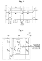
- FIG. 3 is a timing diagram showing the driving of the sustain-discharge circuit of the PDP according to the first embodiment of the present invention.
- sustain-discharge circuit 320 includes sustain-discharge unit 322 and power recovering unit 324.
- Sustain-discharge unit 322 includes switching elements S1 and S2 serially connected to each other between power source Vs and power source -Vs.
- the contact point of switching elements S1 and S2 is connected to an electrode (assumed to be a Y electrode) of a plasma panel (a panel capacitor Cp because the plasma panel operates as capacitive load).
- Power sources Vs and -Vs supply voltages corresponding to Vs and -Vs.
- Another sustain-discharge circuit is connected to another electrode of panel capacitor Cp.
- the power recovering unit 324 includes inductor L connected to the contact point of switching elements S1 and S2 and switching elements S3 and S4. Switching elements S3 and S4 are connected to each other in parallel between the other end of inductor L and ground. Also, power recovering unit 324 can further include diodes D1 and D2 respectively formed on a path between switching element S3 and inductor L and on a path between switching element S4 and inductor L.
- the switching elements S1, S2, S3, and S4 included in sustain-discharge unit 322 and power recovering unit 324 are shown as MOSFETs in FIG. 2. However, the switching elements are not restricted to the MOSFETs and other types of switching elements may be used if the other types of the switching elements perform the same or similar functions.
- the switching elements preferably include body diodes.
- sustain-discharge circuit 320 The operation of sustain-discharge circuit 320 according to the first embodiment of the present invention will now be described with reference to FIG. 3.
- Y electrode voltage Vy of panel capacitor Cp is substantially sustained to be -Vs.
- switching elements S2, S3, and S4 are turned off and switching element S3 is turned on in a mode 1 (M1), an LC resonance is generated in a path of ground, switching element S3, diode D1, inductor L, and panel capacitor Cp.
- Resonance current I L that flows through inductor L by the LC resonance forms a half period of a sine wave.
- Y electrode voltage Vy increases from -Vs to Vs.
- switching element S1 In a mode 2 (M2), switching element S1 is turned on when Y electrode voltage Vy increases to Vs. Accordingly, Y electrode voltage Vy is sustained to be Vs by power source Vs. Switching element S3 can be turned off at this time or in a mode 3 (M3).
- switching element S4 is turned on. Accordingly, the LC resonance is generated in a path of panel capacitor Cp, inductor L, diode D2, switching element S4, and ground. Resonance current I L that flows through inductor L by the LC resonance forms the half period of the sine wave. At this time, Y electrode voltage Vy decreases from Vs to -Vs.
- a mode 4 when Y electrode voltage Vy decreases to -Vs, switching element S2 is turned on. Accordingly, Y electrode voltage Vy is sustained to -Vs by power source -Vs. Switching element S4 can be turned off at this time or in the repeated mode 1 (M1).
- Vs and -Vs can be alternately applied to the Y electrode of the panel capacitor by repeating mode 1 through mode 4.
- the sustain-discharge circuit for applying Vs and -Vs in a polarity opposite to that of the first embodiment is connected to other electrodes (the X electrodes), a voltage loaded on both ends of panel capacitor Cp becomes a voltage 2Vs required for the sustain-discharge. Accordingly, the sustain-discharge may occur in a panel.
- the first embodiment of the present invention it is possible to change the voltage of panel capacitor Cp using the voltage charged to panel capacitor Cp. That is, because current for charging or discharging the panel capacitor needs not be applied from an external power source, unnecessary power is not used.
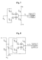
- FIG. 4 is a circuit diagram of a sustain-discharge circuit of a PDP according to a second embodiment of the present invention.
- FIG. 5 is a timing diagram showing the driving of the sustain-discharge circuit according to the second embodiment of the present invention.
- FIG. 6 shows a circuit obtained by modifying the sustain-discharge circuit according to the second embodiment of the present invention.
- sustain-discharge circuit 320 further includes power source unit 326.
- Power source unit 326 includes switching elements S5 and S6. Switching elements S5 and S6 are serially connected to each other between power source Vs and ground. Capacitor Cs is connected between the contact point of switching elements S5 and S6 and switching element S2 of sustain-discharge unit 322. The contact point of switching elements S5 and S6 is connected to switching element S1. Diode Ds is connected between capacitor Cs and ground. Accordingly, voltage -Vs can be applied to panel capacitor Cp using the voltage charged to capacitor Cs without a power source -Vs.
- the driving time according to the second embodiment of the present invention is the same as that of the first embodiment excepting that voltages Vs and -Vs are applied to the Y electrode of panel capacitor Cp by the operations of switching elements S5 and S6.
- switching elements S5 and S6 are turned off in the modes 1 and 3 (M1) and (M3), that is, in the step of changing the voltage of panel capacitor Cp.
- M1 and M3 Y electrode voltage Vy of panel capacitor Cp is sustained to be voltage Vs by turning on switching element S5 in a state where switching element S6 is turned off.
- Voltage Vs is charged to capacitor Cs through a path of power source Vs, switching element S5, capacitor Cs, diode Ds, and ground.
- M4 a path of ground, switching element S6, capacitor Cs, switching element S2, and panel capacitor Cp is formed by turning on switching element S6 in a state where switching element S5 is turned off.
- Voltage -Vs is applied to the Y electrode of panel capacitor Cp by voltage Vs charged to capacitor Cs through the path.
- Y electrode voltage Vy of panel capacitor Cp can maintain voltage -Vs.
- diode Ds is used in order to form the path for charging voltage Vs to capacitor Cs.
- switching element S7 can be used instead of diode Ds as shown in FIG. 6. That is, a path is formed by turning on switching element S7 when voltage Vs is charged to capacitor Cs in the mode 2 (M2). In other cases, the path is intercepted by turning off switching element S7.
- Switching elements S5, S6, and S7 used by power source unit 326 are shown as MOSFETs in FIGS. 4 and 6. However, any switching elements that perform the same or similar functions can be used as the MOSFETs.
- the switching elements preferably include body diodes.
- Inductor L is used in the first and second embodiments of the present invention.
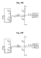
- Two inductors L1 and L2 can be used as shown in FIGS. 7 and 8. That is, inductor L1 can be used in the path formed from ground to the panel capacitor and inductor L2 can be used in the path formed from panel capacitor Cp to ground.
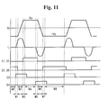
- FIGS. 9 and 11 are timing diagrams showing the driving of sustain-discharge circuits according to third and fourth embodiments of the present invention.
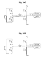
- FIGS. 10A through 10H show the current paths of the respective modes in the sustain-discharge circuit according to the third embodiment of the present invention.
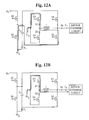
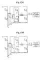
- FIGS. 12A through 12H show the current paths of the respective modes in the sustain-discharge circuit according to the fourth embodiment.
- the sustain-discharge circuit according to the third embodiment of the present invention has the same circuit as that of the first embodiment. Before performing the operation according to the third embodiment of the present invention, it is set that Y electrode voltage Vy of panel capacitor Cp is sustained to be -Vs because switching element S2 is turned on.
- switching element S2 is turned off in a state where switching element S3 is turned on.
- switching element S2 is turned off, as shown in FIG. 10B, current I L that flows from inductor L to power source -Vs flows through panel capacitor Cp because the current path is intercepted. Accordingly, the LC resonance is generated by inductor L and panel capacitor Cp.
- Y electrode voltage Vy of panel capacitor Cp increases from voltage -Vs to voltage Vs due to the energy accumulated in the resonance current and the inductor.
- Y electrode Vy of panel capacitor Cp is sustained to be voltage Vs by turning on switching element S1.
- switching element S1 is turned on in a state where a voltage between a drain and a source is 0, switching element S1 can perform zero voltage switching. Accordingly, the turn-on switching loss of switching element S1 is not generated. Because the energy accumulated in inductor L is used in the third embodiment, it is possible to increase Y electrode voltage Vy to Vs even when a parasitic component exists in the sustain-discharge circuit. That is, the zero voltage switching can be performed even when the parasitic component exists in the circuit.
- switching element S1 continuously is turned on. Accordingly, Y electrode voltage Vy of panel capacitor Cp is continuously sustained to Vs and switching element S3 is turned off when current I L that flows through the inductor decreases to 0A.
- switching element S4 is turned on in a state where switching element S1 is turned on. Accordingly, as shown in FIG. 10E, a current path of power source Vs, switching element S1, inductor L, diode D2, switching element S4, and ground is formed. Current I L that flows through inductor L linearly increases in an opposite direction. Accordingly, energy is accumulated in inductor L.
- a mode 6 M6
- switching element S1 is turned off. Accordingly, as shown in FIG. 10F, the LC resonance path is formed from panel capacitor Cp to inductor L. Therefore, Y electrode voltage Vy of panel capacitor Cp decreases from voltage Vs to voltage -Vs by the energy accumulated in resonance current I L and inductor L.
- Y electrode voltage Vy reaches -Vs and the body diode of switching element S2 conducts. Accordingly, as shown in FIG. 10G, a current path of the body diode of switching element S2, inductor L, diode D2, switching element S4, and ground is formed. Therefore, current I L that flows through inductor L is recovered to ground and linearly decreases to 0A.
- switching element S2 is turned on in a state where the body diode conducts. Accordingly, Y electrode voltage Vy of panel capacitor Cp is sustained to -Vs. At this time, because switching element S2 is turned on in a state where the voltage between the drain and the source is 0, that is, because switching element S2 performs the zero voltage switching, the turn-on switching loss of switching element S2 is not generated.
- Y electrode voltage Vy is continuously sustained to -Vs by continuously turning on switching element S2 and switching element S4 is turned off when current I L that flows through the inductor decreases to 0A.
- the third embodiment of the present invention power is consumed in order to accumulate energy in the inductor in the modes 1 through 5. Power is recovered in the modes 3 through 7. Therefore, because the consumed power is ideally equal to the charged power, the consumed total power becomes 0W. Accordingly, it is possible to change the voltage of the panel capacitor without consuming the power. Because the energy accumulated in the inductor is used when the terminal voltage of the panel capacitor is changed, it is possible to perform the zero voltage switching when the parasitic component exists in the circuit.
- a sustain-discharge circuit obtained by adding power source unit 326 for supplying power sources Vs and -Vs to the sustain-discharge circuit according to the second embodiment of the present invention will be described with reference to FIGS. 11 and 12A through 12H.
- Sustain-discharge circuit 320 has the same circuit as that of the second embodiment. It is set that Y electrode voltage Vy of panel capacitor Cp is sustained to -Vs by voltage Vs charged by capacitor Cs because capacitor Cs is charged by Vs before performing an operation according to the fourth embodiment, and switching elements S2 and S6 are turned on. Because the operation in the fourth embodiment is the same as the operation in the third embodiment excepting that voltages Vs and -Vs are supplied using switching elements S5 and S6, capacitor Cs, and diode Ds, the operations of switching elements S5 and S6 will be described in priority.
- switching element S3 is turned on in a state where switching elements S2 and S6 are turned on. Accordingly, a current path of switching element S3, diode D1, inductor L, switching element S2, capacitor Cs, and switching element S6 is formed. Current I L that flows through inductor L linearly increases by the current path. Accordingly, energy is accumulated in inductor L.
- switching elements S2 and S6 are turned off in a state where switching element S3 is turned on.
- Y electrode voltage Vy of panel capacitor Cp increases from voltage -Vs to voltage Vs by the energy accumulated in the resonance current and inductor L shown in FIG. 12B.
- Y electrode voltage Vy is continuously sustained to be Vs by continuously turning on switching elements S1 and S5.
- Switching element S3 is turned off after current I L that flows through the inductor decreases to 0A.
- switching element S4 is turned on in a state where switching elements S1 and S5 are turned on. Accordingly, as shown in FIG. 12E, a current path of power source Vs, switching elements S5 and S1, inductor L, diode D2, switching element S4, and ground is formed. Current I L that flows through inductor L linearly increases in an opposite direction. Accordingly, energy is accumulated in inductor L.
- switching elements S1 and S5 are turned off in a state where switching element S4 is turned on.
- Y electrode voltage Vy of panel capacitor Cp decreases from voltage Vs to voltage -Vs by the resonance current and the energy accumulated in inductor L, which are shown in FIG. 12F, as described in the mode 6 of the third embodiment.
- the Y electrode voltage Vy is sustained to be -Vs because switching elements S2 and S6 are turned on in a state where the body diode conducts. Because switching elements S2 and S6 perform the zero voltage switching as described in the third embodiment, the turn-on switching loss is not generated.
- Y electrode voltage Vy is continuously sustained to be -Vs by continuously turning on switching elements S2 and S6 and switching element S4 is turned off when current I L that flows through the inductor decreases to 0A.
- switching element S7 can be used instead of diode Ds. In this case, switching element S7 is turned on when switching element S5 is turned on so that capacitor Cs is continuously charged to voltage Vs.
- inductors L1 and L2 can be used as in the first and second embodiments (Refer to FIGS. 7 and 8). That is, inductor L1 is used in the path formed from ground to panel capacitor Cp. Inductor L2 is used in the path formed from one end of panel capacitor Cp to ground.
- inductors of two directions vary, it is possible to set the increasing time and the decreasing time of Y electrode voltage Vy of panel capacitor Cp to be different from each other.
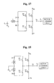
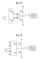
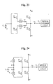
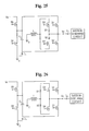
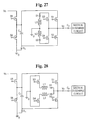
- FIGS. 13 through 29 show the sustain-discharge circuits according to the embodiments of the present invention.
- the sustain-discharge circuits shown in FIGS. 13 through 24 are obtained by modifying the sustain-discharge circuit according to the first or third embodiment of the present invention.
- the sustain-discharge circuits shown in FIGS. 25 through 29 are obtained by modifying the sustain-discharge circuit according to the second or fourth embodiment of the present invention.
- the sustain-discharge circuit according to another embodiment of the present invention is the same as that of the first or third embodiment excepting the position of inductor L.
- Inductor L is connected between the contact point of switching elements S3 and S4 and ground.
- the sustain-discharge circuit according to another embodiment of the present invention is the same as that of the embodiment shown in FIG. 13 excepting the positions of diodes D1 and D2. That is, diodes D1 and D2 are connected to each other between switching elements S3 and S4 and inductor L.
- the sustain-discharge circuits according to other embodiments of the present invention are the same as those of the embodiments shown in FIGS. 2, 13, and 14 excepting voltage magnitudes VH and VL of two power sources and power recovery capacitor Cs.
- the voltage magnitudes of a first sustain power source and a second sustain power source are different from each other in the sustain-discharge circuits shown in FIGS. 15 through 17.
- power recovery capacitor Cc exists. Accordingly, the voltage of (VH+VL)/2 must be charged to capacitor Cc.
- the sustain-discharge circuits according to other embodiments of the present invention are obtained by including two inductors L1 and L2 in the sustain-discharge circuits shown in FIGS. 14, 15, and 17.
- the sustain-discharge circuits according to other embodiments of the present invention are obtained by changing the positions of inductors L1 and L2 into the positions of diodes D1 and D2 in the sustain-discharge circuits shown in FIGS. 7, 18, 19, and 20.
- the sustain-discharge circuit according to another embodiment of the present invention shown in FIG. 25 is the same as the sustain-discharge circuit shown in FIG. 4 excepting the position of inductor L.
- the sustain-discharge circuit according to another embodiment of the present invention shown in FIG. 26 is the same as the sustain-discharge circuit shown in FIG. 25 excepting the positions of diodes D1 and D2.
- the sustain-discharge circuit according to another embodiment of the present invention shown in FIG. 27 is obtained by including two inductors L1 and L2 in the sustain-discharge circuit shown in FIG. 26.
- the sustain-discharge circuits according to other embodiments of the present invention shown in FIGS. 28 and 29 are obtained by changing the positions of inductors L1 and L2 into the positions of diodes D1 and D2 in the sustain-discharge circuits according to the embodiments shown in FIGS. 8 and 27.
- the voltage applied to the Y electrodes of the panel is described in the embodiments of the present invention. However, as mentioned above, the circuit applied to the Y electrodes is applied to the X electrodes. Also, when the applied voltage is changed, the circuit can be applied to an address electrode.
- the sustain-discharge circuit of the PDP according to the present invention can recover power without using a power recovery capacitor having a large capacitance outside the sustain-discharge circuit. Also, because the zero voltage switching can be performed when the parasitic component exists in the circuit, the turn-on loss of the switching element is reduced.
Landscapes
- Engineering & Computer Science (AREA)
- Physics & Mathematics (AREA)
- Power Engineering (AREA)
- Plasma & Fusion (AREA)
- Computer Hardware Design (AREA)
- General Physics & Mathematics (AREA)
- Theoretical Computer Science (AREA)
- Control Of Indicators Other Than Cathode Ray Tubes (AREA)
- Control Of Gas Discharge Display Tubes (AREA)
Abstract
Description
Claims (36)
- A plasma display panel driving circuit for a plasma display panel comprising a plurality of address electrodes, a plurality of a pair of a scan electrode and a sustain electrode alternately arranged, and a panel capacitor formed among the scan electrode, the sustain electrode and the address electrode, the plasma display panel driving circuit comprising:first and second signal lines for supplying first and second voltages, and at least one inductor coupled between one end of the panel capacitor and a third voltage;a first current path for coupling the first signal line to the inductor, so that current of a first direction is supplied to the inductor and first energy is stored in a state where one end of the panel capacitor is substantially sustained to be the first voltage;a second current path for generating a resonance between the inductor and the panel capacitor, and substantially decreasing a voltage of one end of the panel capacitor to the second voltage using current caused by the resonance and the first energy;a third current path for coupling the second signal line to the inductor, so that current of a second direction opposite to the first direction is supplied to the inductor and second energy can be stored in a state where one end of the panel capacitor is substantially sustained to be the second voltage; anda fourth current path for generating a resonance between the inductor and the panel capacitor, and substantially increasing a voltage of one end of the panel capacitor to the first voltage using current caused by the resonance and the second energy.
- The plasma display panel driving circuit of claim 1, wherein energy remains in the inductor when a voltage of one end of the panel capacitor is changed into the first or second voltages.
- The plasma display panel driving circuit of claim 2, further comprising fifth and sixth current paths for recovering the energy remaining in the inductor when the voltage of one end of the panel capacitor is changed into the first and second voltages, respectively.
- The plasma display panel driving circuit of claim 1, wherein the currents of the first and second directions pass through the same inductor.
- The plasma display panel driving circuit of claim 1, wherein the inductor comprises a first inductor, through which the current of the first direction passes, and a second inductor, through which the current of the second direction passes.
- The plasma display panel driving circuit of claim 1, wherein the first and second signal lines are connected to one end of the panel capacitor, so that the voltage of one end of the panel capacitor is sustained to be the first and second voltages, respectively.
- The plasma display panel driving circuit of claim 1, further comprising:first and second switching elements formed on the first and second signal lines, and operating so that the first and third current paths are respectively formed; andthird and fourth switching elements connected in parallel between the inductor and the third voltage, and operating so that the first and second current paths and the third and fourth current paths are formed, respectively.
- The plasma display panel driving circuit of claim 7, wherein the first and second switching elements comprise body diodes.
- The plasma display panel driving circuit of claim 1, wherein the third voltage corresponds to a half of the sum of the first and second voltages.
- The plasma display panel driving circuit of claim 9, wherein the first and second voltages have the same magnitude, and electric potentials that are opposite to each other, and the third voltage is a ground voltage.
- The plasma display panel driving circuit of claim 10, further comprising a capacitor whose one end is selectively coupled to a first power source supplying the first voltage and a ground,
wherein the first signal line is coupled to the first power source,
and wherein the second signal line is coupled to the other end of a capacitor charged by the first voltage. - The plasma display panel driving circuit of claim 10, wherein the first signal line comprises a first switching element coupled between a first power source supplying the first voltage and one end of the panel capacitor,
and wherein the second signal line further comprises a second switching element connected between a ground and the first switching element and a capacitor coupled between the contact point of the first and second switching elements and one end of the panel capacitor. - A plasma display panel driving circuit for a plasma display panel comprising a plurality of address electrodes, a plurality of a pair of a scan electrode and a sustain electrode alternately arranged, and a panel capacitor formed among the scan electrode, the sustain electrode and the address electrode, the plasma display panel driving circuit comprising:first and second signal lines for supplying a first voltage and a second voltage having a level opposite to the level of the first voltage, and at least an inductor coupled between one end of the panel capacitor and a ground;a first current path between one end of the panel capacitor substantially sustained to the first voltage by the first signal line and ground, the first current path for generating a resonance between the inductor and the panel capacitor, thereby substantially decreasing a voltage of one end of the panel capacitor to the second voltage; anda second current path between one end of the panel capacitor substantially sustained to the second voltage by the second signal line and ground, the second current path for generating a resonance between the inductor and the panel capacitor, thereby substantially increasing a voltage of one end of the panel capacitor to the first voltage.
- The plasma display panel driving circuit of claim 13, wherein the current of the first and second directions passes through the same inductor.
- The plasma display panel driving circuit of claim 13, wherein the inductor comprises a first inductor, through which the current of the first direction passes, and a second inductor, through which the current of the second direction passes.
- The plasma display panel driving circuit of claim 13, further comprising:first and second switching elements connected in parallel between ground and the inductor, and operating so that the first and second current paths are formed, respectively; andthird and fourth switching elements formed on the first and second signal lines and operating so that a voltage of one end of the panel capacitor is fixed to the first and second voltages, respectively.
- The plasma display panel driving circuit of claim 16, wherein the third and fourth switching elements comprise body diodes.
- The plasma display panel driving circuit of claim 13, further comprising a capacitor selectively coupled to a first power source supplying the first voltage and ground,
wherein the first signal line is coupled to the first power source,
and wherein the second signal line is coupled by the first power source to the other end of the capacitor charged by the first voltage. - The plasma display panel driving circuit of claim 13, wherein the first signal line comprises a first switching element coupled between a first power source supplying the first voltage and one end of the panel capacitor,
and wherein the second signal line comprises a second switching element connected between ground and the first switching element and a capacitor coupled between the contact point of the first and second switching elements and one end of the panel capacitor. - A plasma display panel driving circuit for a plasma display panel comprising a plurality of address electrodes, a plurality of a pair of a scan electrode and a sustain electrode alternately arranged, and a panel capacitor formed among the scan electrode, the sustain electrode and the address electrode, the plasma display panel driving circuit comprising:first and second switching elements, which are serially connected between a first signal line and a second signal line respectively supplying a first voltage and a second voltage having opposite levels and whose contact point is coupled to one end of the panel capacitor;at least one inductor coupled to one end of the panel capacitor; andthird and fourth switching elements connected to each other between ground and the inductor in parallel.
- The plasma display panel driving circuit of claim 20, further comprising a capacitor whose one end is selectively coupled to a power source supplying the first voltage and ground,
wherein the first signal line is coupled to the power source,
and wherein the second signal line is coupled to the other end of the capacitor charged by the first voltage. - The plasma display panel driving circuit of claim 20, wherein the first signal line comprises a fifth switching element coupled between a power source supplying the first voltage and one end of the panel capacitor,
and wherein the second signal line further comprises a sixth switching element connected between a ground and the fifth switching element and a capacitor coupled between the contact point of the fifth and sixth switching elements and one end of the panel capacitor. - The plasma display panel driving circuit of claim 20, wherein the first and second switching elements comprise body diodes.
- A plasma display panel driving circuit for a plasma display panel comprising a plurality of address electrodes, a plurality of a pair of a scan electrode and a sustain electrode alternately arranged, and a panel capacitor formed among the scan electrode, the sustain electrode and the address electrode, the plasma display panel driving circuit comprising:wherein first and second energies are stored in the inductor through first and second current paths formed through the third voltage and the first and second signal lines and the panel capacitor is discharged and charged using the first and second energies.first and second switching elements, which are serially connected between first and second signal lines respectively supplying first and second voltages and whose contact point is coupled to one end of the panel capacitor;at least one inductor coupled to one end of the panel capacitor; andthird and fourth switching elements connected in parallel between a third voltage that is an intermediate voltage of the first and second voltages and the inductor;
- The plasma display panel driving circuit of claim 24, further comprising a capacitor whose one end is selectively coupled to a power source supplying the first voltage and ground,
wherein the first signal line is coupled to the power source,
and wherein the second signal line is coupled to the other end of the capacitor charged by the first voltage. - The plasma display panel driving circuit of claim 25, wherein the first signal line further comprises a fifth switching element connected between the power source and the first switching element,
wherein the second signal line comprises a sixth switching element coupled between one end of the panel capacitor and ground,
and wherein the other end of the capacitor is coupled to ground when the fifth switching element is turned on. - The plasma display panel driving circuit of claim 24, wherein the first and second switching elements comprise body diodes.
- A method for driving a plasma display panel including a panel capacitor, at least one inductor coupled to one end of the panel capacitor, and first and second signal lines supplying a first voltage and a second voltage of a level lower than the level of the first voltage to one end of the panel capacitor, the method comprising:(a) storing energy in the inductor through a path formed between a third voltage that is a voltage between the first and second voltages and the first signal line in a state where a voltage of one end of the panel capacitor is substantially sustained to the first voltage;(b) decreasing a voltage of one end of the panel capacitor to substantially the second voltage using resonance current generated between the inductor and the panel capacitor and the energy stored in the step (a);(c) storing energy in the inductor through a path formed between the second line and the third voltage in a state where a voltage of one end of the panel capacitor is substantially sustained to the second voltage; and(d) increasing a voltage of one end of the panel capacitor to substantially the first voltage using the resonance current generated between the inductor and the panel capacitor and the energy stored in the step (c).
- The method of claim 28, wherein energy exists in the inductor when the voltage of the panel capacitor changes into the second and first voltages, respectively in the steps (b) and (d).
- The method of claim 29, wherein the steps (b) and (d) further comprise the step of recovering the energy remaining in the inductor after changing the voltage of one end of the panel capacitor into the second and first voltages.
- The method of claim 28, wherein the inductors, in which energies are stored in the steps (a) and (c), are the same inductor.
- The method of claim 28, wherein the inductor comprises first and second inductors and the energies are stored in the first and second inductors in the steps (a) and (c).
- A plasma display panel apparatus, comprising:wherein the driving circuit includes:a plasma panel including a plurality of address electrodes arranged in a first direction, and a plurality of a pair of a first electrode and a second electrode alternately arranged in a second direction; anda driving circuit that sends a driving signal to the first electrode, the second electrode and the address electrode,first and second signal lines for supplying first and second voltages, and at least one inductor coupled between one end of a panel capacitor of the plasma panel and a third voltage;a first current path for coupling the first signal line to the inductor, so that current of a first direction is supplied to the inductor and first energy is stored in a state where one end of the panel capacitor is substantially sustained to be the first voltage;a second current path for generating a resonance between the inductor and the panel capacitor, and substantially decreasing a voltage of one end of the panel capacitor to the second voltage using current caused by the resonance and the first energy;a third current path for coupling the second signal line to the inductor, so that current of a second direction opposite to the first direction is supplied to the inductor and second energy can be stored in a state where one end of the panel capacitor is substantially sustained to be the second voltage; anda fourth current path for generating a resonance between the inductor and the panel capacitor, and substantially increasing a voltage of one end of the panel capacitor to the first voltage using current caused by the resonance and the second energy.
- A plasma display panel apparatus, comprising:wherein the driving circuit includes:a plasma panel including a plurality of address electrodes arranged in a first direction, and a plurality of a pair of a first electrode and a second electrode alternately arranged in a second direction; anda driving circuit that sends a driving signal to the first electrode, the second electrode and the address electrode,first and second signal lines for supplying a first voltage and a second voltage having a level opposite to the level of the first voltage, and at least an inductor coupled between one end of a panel capacitor of the plasma panel and a ground;a first current path between one end of the panel capacitor substantially sustained to the first voltage by the first signal line and ground, the first current path for generating a resonance between the inductor and the panel capacitor, thereby substantially decreasing a voltage of one end of the panel capacitor to the second voltage; anda second current path between one end of the panel capacitor substantially sustained to the second voltage by the second signal line and ground, the second current path for generating a resonance between the inductor and the panel capacitor, thereby substantially increasing a voltage of one end of the panel capacitor to the first voltage.
- A plasma display panel apparatus, comprising:wherein the driving circuit includes:a plasma panel including a plurality of address electrodes arranged in a first direction, and a plurality of a pair of a first electrode and a second electrode alternately arranged in a second direction; anda driving circuit that sends a driving signal to the first electrode, the second electrode and the address electrode,first and second switching elements, which are serially connected between a first signal line and a second signal line respectively supplying a first voltage and a second voltage having opposite levels and whose contact point is coupled to one end of a panel capacitor of the plasma panel;at least one inductor coupled to one end of the panel capacitor; and third and fourth switching elements connected to each other between ground and the inductor in parallel.
- A plasma display panel apparatus, comprising:wherein the driving circuit includes:a plasma panel including a plurality of address electrodes arranged in a first direction, and a plurality of a pair of a first electrode and a second electrode alternately arranged in a second direction; anda driving circuit that sends a driving signal to the first electrode, the second electrode and the address electrode,wherein first and second energies are stored in the inductor through first and second current paths formed through the third voltage and the first and second signal lines and the panel capacitor is discharged and charged using the first and second energies.first and second switching elements, which are serially connected between first and second signal lines respectively supplying first and second voltages and whose contact point is coupled to one end of the panel capacitor;at least one inductor coupled to one end of the panel capacitor; andthird and fourth switching elements connected in parallel between a third voltage that is an intermediate voltage of the first and second voltages and the inductor;
Priority Applications (1)
| Application Number | Priority Date | Filing Date | Title |
|---|---|---|---|
| EP05006098A EP1542200B1 (en) | 2001-08-06 | 2002-08-05 | Apparatus for and method of driving a sustain-discharge circuit of a plasma display panel |
Applications Claiming Priority (4)
| Application Number | Priority Date | Filing Date | Title |
|---|---|---|---|
| KR10-2001-0047311A KR100428624B1 (en) | 2001-08-06 | 2001-08-06 | Ac plasma display panel of sustain circuit |
| KR2001047311 | 2001-08-06 | ||
| KR2002013573 | 2002-03-13 | ||
| KR10-2002-0013573A KR100454025B1 (en) | 2002-03-13 | 2002-03-13 | Plasma display panel and driving apparatus thereof and driving method thereof |
Related Child Applications (1)
| Application Number | Title | Priority Date | Filing Date |
|---|---|---|---|
| EP05006098A Division EP1542200B1 (en) | 2001-08-06 | 2002-08-05 | Apparatus for and method of driving a sustain-discharge circuit of a plasma display panel |
Publications (3)
| Publication Number | Publication Date |
|---|---|
| EP1291836A2 true EP1291836A2 (en) | 2003-03-12 |
| EP1291836A3 EP1291836A3 (en) | 2003-11-05 |
| EP1291836B1 EP1291836B1 (en) | 2007-04-04 |
Family
ID=26639280
Family Applications (2)
| Application Number | Title | Priority Date | Filing Date |
|---|---|---|---|
| EP02017000A Expired - Lifetime EP1291836B1 (en) | 2001-08-06 | 2002-08-05 | Apparatus for and method of driving a plasma display panel |
| EP05006098A Expired - Lifetime EP1542200B1 (en) | 2001-08-06 | 2002-08-05 | Apparatus for and method of driving a sustain-discharge circuit of a plasma display panel |
Family Applications After (1)
| Application Number | Title | Priority Date | Filing Date |
|---|---|---|---|
| EP05006098A Expired - Lifetime EP1542200B1 (en) | 2001-08-06 | 2002-08-05 | Apparatus for and method of driving a sustain-discharge circuit of a plasma display panel |
Country Status (5)
| Country | Link |
|---|---|
| US (4) | US6963174B2 (en) |
| EP (2) | EP1291836B1 (en) |
| JP (1) | JP5042433B2 (en) |
| CN (1) | CN100341039C (en) |
| DE (1) | DE60219247T2 (en) |
Families Citing this family (49)
| Publication number | Priority date | Publication date | Assignee | Title |
|---|---|---|---|---|
| TW482991B (en) * | 2000-09-13 | 2002-04-11 | Acer Display Tech Inc | Power-saving driving circuit for plasma display panel |
| US6963174B2 (en) * | 2001-08-06 | 2005-11-08 | Samsung Sdi Co., Ltd. | Apparatus and method for driving a plasma display panel |
| US6924779B2 (en) * | 2002-03-18 | 2005-08-02 | Samsung Sdi Co., Ltd. | PDP driving device and method |
| KR100458572B1 (en) * | 2002-07-09 | 2004-12-03 | 삼성에스디아이 주식회사 | Plasm display panel and driving method thereof |
| JP2005535914A (en) * | 2002-08-12 | 2005-11-24 | コーニンクレッカ フィリップス エレクトロニクス エヌ ヴィ | Electroluminescent display |
| CN1689061A (en) * | 2002-10-02 | 2005-10-26 | 富士通日立等离子显示器股份有限公司 | Drive circuit and drive method |
| JP2004133406A (en) * | 2002-10-11 | 2004-04-30 | Samsung Sdi Co Ltd | Driving apparatus and driving method for plasma display panel |
| KR100467458B1 (en) * | 2002-10-22 | 2005-01-24 | 삼성에스디아이 주식회사 | Apparatus and method for driving plasm display panel |
| EP1469445A3 (en) | 2003-04-16 | 2009-03-04 | Lg Electronics Inc. | Energy recovering apparatus and method for driving a plasma display panel |
| JP4510422B2 (en) * | 2003-06-12 | 2010-07-21 | パナソニック株式会社 | Capacitive light emitting device driving apparatus |
| KR100508255B1 (en) * | 2003-07-15 | 2005-08-18 | 엘지전자 주식회사 | Energy Recovery Circuit and Driving Method Thereof |
| KR100502931B1 (en) * | 2003-07-30 | 2005-07-21 | 삼성에스디아이 주식회사 | Driving device and method of plasma display panel and plasma display device |
| KR100503806B1 (en) * | 2003-08-06 | 2005-07-26 | 삼성전자주식회사 | Plasma display panel sustain driver for decreasing flywheel current |
| US7287212B2 (en) * | 2003-09-26 | 2007-10-23 | Broadcom Corporation | Methods and systems for Viterbi decoding |
| KR100521489B1 (en) * | 2003-10-06 | 2005-10-12 | 삼성에스디아이 주식회사 | Driving apparatus and method of plasma display panel and plasma display device |
| KR100542235B1 (en) * | 2003-10-16 | 2006-01-10 | 삼성에스디아이 주식회사 | Plasma Display Panel and Driving Device thereof |
| KR20050037639A (en) | 2003-10-20 | 2005-04-25 | 엘지전자 주식회사 | Energy recovering apparatus |
| KR100542226B1 (en) * | 2003-10-24 | 2006-01-10 | 삼성에스디아이 주식회사 | Driving apparatus and driving method of plasma display panel |
| KR100560471B1 (en) * | 2003-11-10 | 2006-03-13 | 삼성에스디아이 주식회사 | Plasma Display Panel and Driving Method thereof |
| KR100550983B1 (en) * | 2003-11-26 | 2006-02-13 | 삼성에스디아이 주식회사 | Driving Method of Plasma Display and Plasma Display Panel |
| KR100550985B1 (en) * | 2003-11-28 | 2006-02-13 | 삼성에스디아이 주식회사 | Driving Method of Plasma Display and Plasma Display Panel |
| KR100536221B1 (en) * | 2004-01-30 | 2005-12-12 | 삼성에스디아이 주식회사 | A plasma display device and a driving method of the same |
| CN100349197C (en) * | 2004-03-25 | 2007-11-14 | 东南大学 | Double polar energy restoring and retaining driving gear |
| JP2005316132A (en) * | 2004-04-28 | 2005-11-10 | Mitsubishi Electric Corp | Flat panel display device and semiconductor element used therefor |
| KR100625498B1 (en) * | 2004-05-21 | 2006-09-20 | 엘지전자 주식회사 | Plasma Display Panel Driver |
| KR100529095B1 (en) * | 2004-05-25 | 2005-11-15 | 삼성에스디아이 주식회사 | Driving apparatus of plasma display panel and method thereof |
| KR100625577B1 (en) * | 2004-08-11 | 2006-09-20 | 엘지전자 주식회사 | Driving device of plasma display panel |
| KR100627388B1 (en) * | 2004-09-01 | 2006-09-21 | 삼성에스디아이 주식회사 | Plasma Display and Driving Method |
| KR100612508B1 (en) * | 2004-09-07 | 2006-08-14 | 엘지전자 주식회사 | Driving device of plasma display panel |
| CN100395799C (en) * | 2004-10-18 | 2008-06-18 | 南京Lg同创彩色显示系统有限责任公司 | Energy reclaiming device and method |
| KR100588019B1 (en) * | 2004-12-31 | 2006-06-12 | 엘지전자 주식회사 | Energy recovery device and method of plasma display panel |
| KR100586606B1 (en) * | 2005-03-09 | 2006-06-07 | 엘지전자 주식회사 | Setup voltage generator for sustain driving of plasma display panel |
| US20060267875A1 (en) * | 2005-05-27 | 2006-11-30 | Bi-Hsien Chen | Plasma display panel having less impedance in the sink discharge current path |
| US7733304B2 (en) * | 2005-08-02 | 2010-06-08 | Samsung Sdi Co., Ltd. | Plasma display and plasma display driver and method of driving plasma display |
| KR20070036390A (en) * | 2005-09-29 | 2007-04-03 | 엘지전자 주식회사 | Apparatus and method for driving a plasma display panel |
| JP2007103017A (en) * | 2005-09-30 | 2007-04-19 | Fujitsu Hitachi Plasma Display Ltd | Plasma display device |
| KR100811536B1 (en) * | 2005-10-14 | 2008-03-07 | 엘지전자 주식회사 | Driving device of plasma display panel including sustain driving circuit of improved efficiency |
| TWI299153B (en) * | 2005-10-24 | 2008-07-21 | Chunghwa Picture Tubes Ltd | Circuit and method for resetting plasma display panel |
| KR100800521B1 (en) * | 2006-08-10 | 2008-02-04 | 엘지전자 주식회사 | Plasma display device and driving method thereof |
| KR100877818B1 (en) | 2006-08-10 | 2009-01-12 | 엘지전자 주식회사 | Plasma display device |
| KR100869795B1 (en) | 2006-11-02 | 2008-11-21 | 삼성에스디아이 주식회사 | Plasma display device and driving method thereof |
| US20080136800A1 (en) * | 2006-12-12 | 2008-06-12 | Choi Jeongpil | Plasma display apparatus |
| KR101174718B1 (en) * | 2007-09-20 | 2012-08-21 | 주식회사 오리온 | Driving circuit of plasma display panel and driving method thereof |
| KR100907390B1 (en) * | 2007-11-16 | 2009-07-10 | 삼성에스디아이 주식회사 | Plasma display device |
| US20100026672A1 (en) * | 2008-08-01 | 2010-02-04 | Yoo-Jin Song | Circuit for driving a plasma display panel |
| US20100033406A1 (en) * | 2008-08-11 | 2010-02-11 | Jin-Ho Yang | Plasma display and driving apparatus thereof |
| DE102010048737B4 (en) | 2010-10-16 | 2018-06-28 | Mekra Lang Gmbh & Co. Kg | Interface for vehicle attachment parts, fastening system and mirror device |
| CN103869516B (en) | 2014-03-12 | 2016-04-06 | 京东方科技集团股份有限公司 | display panel discharge circuit and display device |
| GB201715542D0 (en) | 2017-09-22 | 2017-11-08 | Dumas Pierre | Human-powered aircraft |
Family Cites Families (37)
| Publication number | Priority date | Publication date | Assignee | Title |
|---|---|---|---|---|
| US5081400A (en) | 1986-09-25 | 1992-01-14 | The Board Of Trustees Of The University Of Illinois | Power efficient sustain drivers and address drivers for plasma panel |
| US4866349A (en) * | 1986-09-25 | 1989-09-12 | The Board Of Trustees Of The University Of Illinois | Power efficient sustain drivers and address drivers for plasma panel |
| US6028573A (en) * | 1988-08-29 | 2000-02-22 | Hitachi, Ltd. | Driving method and apparatus for display device |
| DE4321945A1 (en) * | 1993-07-02 | 1995-01-12 | Thomson Brandt Gmbh | Alternating voltage generator for controlling a plasma display screen |
| JP2891280B2 (en) * | 1993-12-10 | 1999-05-17 | 富士通株式会社 | Driving device and driving method for flat display device |
| JP2755201B2 (en) * | 1994-09-28 | 1998-05-20 | 日本電気株式会社 | Drive circuit for plasma display panel |
| US5642018A (en) * | 1995-11-29 | 1997-06-24 | Plasmaco, Inc. | Display panel sustain circuit enabling precise control of energy recovery |
| FR2744275B1 (en) * | 1996-01-30 | 1998-03-06 | Thomson Csf | METHOD FOR CONTROLLING A VIEWING PANEL AND VIEWING DEVICE USING THE SAME |
| JP3226815B2 (en) | 1996-03-08 | 2001-11-05 | 日本電気株式会社 | Driving circuit and driving method for capacitive load |
| JP3672669B2 (en) * | 1996-05-31 | 2005-07-20 | 富士通株式会社 | Driving device for flat display device |
| FR2750525B1 (en) * | 1996-06-28 | 1998-09-18 | Thomson Csf | METHOD FOR ACTIVATING CELLS OF AN IMAGE VIEWING SCREEN, AND IMAGE VIEWING DEVICE IMPLEMENTING THE METHOD |
| JP3596197B2 (en) * | 1996-11-18 | 2004-12-02 | 三菱電機株式会社 | Plasma display device |
| KR100222203B1 (en) * | 1997-03-17 | 1999-10-01 | 구자홍 | Energy Recovery Sustain Circuit for AC Plasma Display Panels |
| JP3897896B2 (en) * | 1997-07-16 | 2007-03-28 | 三菱電機株式会社 | Plasma display panel driving method and plasma display device |
| DE19737662A1 (en) * | 1997-08-29 | 1999-03-04 | Thomson Brandt Gmbh | Alternating voltage generator for controlling a plasma display screen |
| JP3568098B2 (en) * | 1998-06-03 | 2004-09-22 | パイオニア株式会社 | Display panel drive |
| JP3114865B2 (en) * | 1998-06-04 | 2000-12-04 | 日本電気株式会社 | Driving device for plasma display panel |
| JP2000047634A (en) * | 1998-07-29 | 2000-02-18 | Pioneer Electron Corp | Driving method of plasma display device |
| JP3399852B2 (en) * | 1998-09-30 | 2003-04-21 | 三菱電機株式会社 | Display panel drive circuit |
| US6160531A (en) * | 1998-10-07 | 2000-12-12 | Acer Display Technology, Inc. | Low loss driving circuit for plasma display panel |
| US6150999A (en) | 1998-10-07 | 2000-11-21 | Acer Display Technology, Inc. | Energy recovery driving circuit for driving a plasma display unit |
| JP3201603B1 (en) | 1999-06-30 | 2001-08-27 | 富士通株式会社 | Driving device, driving method, and driving circuit for plasma display panel |
| CN1122252C (en) * | 1999-08-12 | 2003-09-24 | 友达光电股份有限公司 | Driving Circuit of Plasma Display Panel |
| JP3369535B2 (en) * | 1999-11-09 | 2003-01-20 | 松下電器産業株式会社 | Plasma display device |
| JP3274444B2 (en) * | 1999-11-09 | 2002-04-15 | 松下電器産業株式会社 | Drive circuit and display device |
| DE60022481T2 (en) * | 1999-11-12 | 2006-06-08 | Matsushita Electric Industrial Co., Ltd., Kadoma | PLASMA DISPLAY DEVICE AND METHOD FOR THEIR CONTROL |
| JP3603712B2 (en) | 1999-12-24 | 2004-12-22 | 日本電気株式会社 | Driving apparatus for plasma display panel and driving method thereof |
| US6483490B1 (en) * | 2000-03-22 | 2002-11-19 | Acer Display Technology, Inc. | Method and apparatus for providing sustaining waveform for plasma display panel |
| KR100363679B1 (en) * | 2000-04-19 | 2002-12-05 | 엘지전자 주식회사 | Method Of Driving Plasma Display Panel |
| TW526459B (en) | 2000-06-23 | 2003-04-01 | Au Optronics Corp | Plasma display holding-stage driving circuit with discharging current compensation function |
| KR100365693B1 (en) * | 2000-09-26 | 2002-12-26 | 삼성에스디아이 주식회사 | AC plasma display panel of sustain circuit |
| US6963174B2 (en) * | 2001-08-06 | 2005-11-08 | Samsung Sdi Co., Ltd. | Apparatus and method for driving a plasma display panel |
| KR100421014B1 (en) * | 2001-08-28 | 2004-03-04 | 삼성전자주식회사 | Energy recovery apparatus and energy recovery circuit design method using a coupled inductor in the plasma display panel drive system |
| KR100477985B1 (en) * | 2001-10-29 | 2005-03-23 | 삼성에스디아이 주식회사 | A plasma display panel, a driving apparatus and a method of the plasma display panel |
| US6850213B2 (en) * | 2001-11-09 | 2005-02-01 | Matsushita Electric Industrial Co., Ltd. | Energy recovery circuit for driving a capacitive load |
| KR100502905B1 (en) * | 2002-05-30 | 2005-07-25 | 삼성에스디아이 주식회사 | Driving apparatus and method of plasma display panel |
| KR100477990B1 (en) * | 2002-09-10 | 2005-03-23 | 삼성에스디아이 주식회사 | Plasma display panel and driving apparatus and method thereof |
-
2002
- 2002-07-31 US US10/210,766 patent/US6963174B2/en not_active Expired - Fee Related
- 2002-08-05 EP EP02017000A patent/EP1291836B1/en not_active Expired - Lifetime
- 2002-08-05 EP EP05006098A patent/EP1542200B1/en not_active Expired - Lifetime
- 2002-08-05 DE DE60219247T patent/DE60219247T2/en not_active Expired - Lifetime
- 2002-08-05 JP JP2002228035A patent/JP5042433B2/en not_active Expired - Fee Related
- 2002-08-06 CN CNB021276560A patent/CN100341039C/en not_active Expired - Fee Related
-
2005
- 2005-05-26 US US11/138,758 patent/US7161565B2/en not_active Expired - Fee Related
- 2005-10-21 US US11/256,401 patent/US7483000B2/en not_active Expired - Fee Related
-
2006
- 2006-11-30 US US11/607,449 patent/US7839358B2/en not_active Expired - Fee Related
Also Published As
| Publication number | Publication date |
|---|---|
| US20050270255A1 (en) | 2005-12-08 |
| US7839358B2 (en) | 2010-11-23 |
| EP1542200A3 (en) | 2009-04-29 |
| EP1542200A2 (en) | 2005-06-15 |
| CN1405747A (en) | 2003-03-26 |
| CN100341039C (en) | 2007-10-03 |
| JP5042433B2 (en) | 2012-10-03 |
| JP2003108064A (en) | 2003-04-11 |
| EP1291836B1 (en) | 2007-04-04 |
| US20060033685A1 (en) | 2006-02-16 |
| EP1542200B1 (en) | 2012-11-21 |
| US7161565B2 (en) | 2007-01-09 |
| US6963174B2 (en) | 2005-11-08 |
| DE60219247T2 (en) | 2008-01-03 |
| EP1291836A3 (en) | 2003-11-05 |
| DE60219247D1 (en) | 2007-05-16 |
| US7483000B2 (en) | 2009-01-27 |
| US20030025459A1 (en) | 2003-02-06 |
| US20070109228A1 (en) | 2007-05-17 |
Similar Documents
| Publication | Publication Date | Title |
|---|---|---|
| EP1542200B1 (en) | Apparatus for and method of driving a sustain-discharge circuit of a plasma display panel | |
| KR100463187B1 (en) | Plasm display panel and driving apparatus and driving method thereof | |
| US6924779B2 (en) | PDP driving device and method | |
| US20030071768A1 (en) | Plasma display panel and method for driving the same | |
| KR100458571B1 (en) | Driving apparatus and method of plasm display panel | |
| KR100458572B1 (en) | Plasm display panel and driving method thereof | |
| US7170474B2 (en) | Plasma display panel driver, driving method thereof, and plasma display device | |
| US6707258B2 (en) | Plasma display panel driving method and apparatus | |
| CN101013555B (en) | Apparatus for and method of driving a plasma display panel | |
| KR100453892B1 (en) | driver circuit of plasma display panel comprising scan voltage generator circuit | |
| KR100627388B1 (en) | Plasma Display and Driving Method | |
| KR100740112B1 (en) | Plasma Display, Driving Device and Driving Method | |
| KR100454025B1 (en) | Plasma display panel and driving apparatus thereof and driving method thereof | |
| KR100521482B1 (en) | A driving method of plasma display panel | |
| KR100649193B1 (en) | Plasma display device and driving method thereof | |
| KR20050120201A (en) | A driving method of plasma display panel and plasma display device |
Legal Events
| Date | Code | Title | Description |
|---|---|---|---|
| PUAI | Public reference made under article 153(3) epc to a published international application that has entered the european phase |
Free format text: ORIGINAL CODE: 0009012 |
|
| AK | Designated contracting states |
Designated state(s): AT BE BG CH CY CZ DE DK EE ES FI FR GB GR IE IT LI LU MC NL PT SE SK TR Kind code of ref document: A2 Designated state(s): AT BE BG CH CY CZ DE DK EE ES FI FR GB GR IE IT LI LU MC NL PT SE SK TR |
|
| AX | Request for extension of the european patent |
Extension state: AL LT LV MK RO SI |
|
| PUAL | Search report despatched |
Free format text: ORIGINAL CODE: 0009013 |
|
| AK | Designated contracting states |
Kind code of ref document: A3 Designated state(s): AT BE BG CH CY CZ DE DK EE ES FI FR GB GR IE IT LI LU MC NL PT SE SK TR |
|
| AX | Request for extension of the european patent |
Extension state: AL LT LV MK RO SI |
|
| 17P | Request for examination filed |
Effective date: 20040301 |
|
| AKX | Designation fees paid |
Designated state(s): DE FR GB NL |
|
| 17Q | First examination report despatched |
Effective date: 20040729 |
|
| RTI1 | Title (correction) |
Free format text: APPARATUS FOR AND METHOD OF DRIVING A PLASMA DISPLAY PANEL |
|
| GRAP | Despatch of communication of intention to grant a patent |
Free format text: ORIGINAL CODE: EPIDOSNIGR1 |
|
| GRAS | Grant fee paid |
Free format text: ORIGINAL CODE: EPIDOSNIGR3 |
|
| GRAA | (expected) grant |
Free format text: ORIGINAL CODE: 0009210 |
|
| AK | Designated contracting states |
Kind code of ref document: B1 Designated state(s): DE FR GB NL |
|
| REG | Reference to a national code |
Ref country code: GB Ref legal event code: FG4D |
|
| REF | Corresponds to: |
Ref document number: 60219247 Country of ref document: DE Date of ref document: 20070516 Kind code of ref document: P |
|
| ET | Fr: translation filed | ||
| PLBE | No opposition filed within time limit |
Free format text: ORIGINAL CODE: 0009261 |
|
| STAA | Information on the status of an ep patent application or granted ep patent |
Free format text: STATUS: NO OPPOSITION FILED WITHIN TIME LIMIT |
|
| 26N | No opposition filed |
Effective date: 20080107 |
|
| PGFP | Annual fee paid to national office [announced via postgrant information from national office to epo] |
Ref country code: GB Payment date: 20130626 Year of fee payment: 12 |
|
| PGFP | Annual fee paid to national office [announced via postgrant information from national office to epo] |
Ref country code: DE Payment date: 20130626 Year of fee payment: 12 Ref country code: NL Payment date: 20130626 Year of fee payment: 12 |
|
| PGFP | Annual fee paid to national office [announced via postgrant information from national office to epo] |
Ref country code: FR Payment date: 20130718 Year of fee payment: 12 |
|
| REG | Reference to a national code |
Ref country code: DE Ref legal event code: R119 Ref document number: 60219247 Country of ref document: DE |
|
| REG | Reference to a national code |
Ref country code: NL Ref legal event code: V1 Effective date: 20150301 |
|
| GBPC | Gb: european patent ceased through non-payment of renewal fee |
Effective date: 20140805 |
|
| PG25 | Lapsed in a contracting state [announced via postgrant information from national office to epo] |
Ref country code: NL Free format text: LAPSE BECAUSE OF NON-PAYMENT OF DUE FEES Effective date: 20150301 |
|
| REG | Reference to a national code |
Ref country code: FR Ref legal event code: ST Effective date: 20150430 |
|
| REG | Reference to a national code |
Ref country code: DE Ref legal event code: R119 Ref document number: 60219247 Country of ref document: DE Effective date: 20150303 |
|
| PG25 | Lapsed in a contracting state [announced via postgrant information from national office to epo] |
Ref country code: DE Free format text: LAPSE BECAUSE OF NON-PAYMENT OF DUE FEES Effective date: 20150303 Ref country code: GB Free format text: LAPSE BECAUSE OF NON-PAYMENT OF DUE FEES Effective date: 20140805 |
|
| PG25 | Lapsed in a contracting state [announced via postgrant information from national office to epo] |
Ref country code: FR Free format text: LAPSE BECAUSE OF NON-PAYMENT OF DUE FEES Effective date: 20140901 |