EP1289121A1 - Low consumption inverter oscillator circiut - Google Patents
Low consumption inverter oscillator circiut Download PDFInfo
- Publication number
- EP1289121A1 EP1289121A1 EP01203052A EP01203052A EP1289121A1 EP 1289121 A1 EP1289121 A1 EP 1289121A1 EP 01203052 A EP01203052 A EP 01203052A EP 01203052 A EP01203052 A EP 01203052A EP 1289121 A1 EP1289121 A1 EP 1289121A1
- Authority
- EP
- European Patent Office
- Prior art keywords
- inverter
- oscillator circuit
- resonator
- transconductance value
- mos transistor
- Prior art date
- Legal status (The legal status is an assumption and is not a legal conclusion. Google has not performed a legal analysis and makes no representation as to the accuracy of the status listed.)
- Withdrawn
Links
- 238000009499 grossing Methods 0.000 claims abstract description 7
- 239000003990 capacitor Substances 0.000 claims abstract description 6
- 238000005452 bending Methods 0.000 claims description 9
- 239000010453 quartz Substances 0.000 claims description 8
- VYPSYNLAJGMNEJ-UHFFFAOYSA-N silicon dioxide Inorganic materials O=[Si]=O VYPSYNLAJGMNEJ-UHFFFAOYSA-N 0.000 claims description 8
- 238000000034 method Methods 0.000 claims description 6
- 239000012321 sodium triacetoxyborohydride Substances 0.000 claims description 3
- 230000010355 oscillation Effects 0.000 description 18
- 238000010586 diagram Methods 0.000 description 6
- 230000009467 reduction Effects 0.000 description 5
- 238000012423 maintenance Methods 0.000 description 4
- 230000006872 improvement Effects 0.000 description 3
- 230000009471 action Effects 0.000 description 2
- 238000013016 damping Methods 0.000 description 2
- 230000000694 effects Effects 0.000 description 2
- 230000004048 modification Effects 0.000 description 2
- 238000012986 modification Methods 0.000 description 2
- 230000005540 biological transmission Effects 0.000 description 1
- 230000008859 change Effects 0.000 description 1
- 230000000295 complement effect Effects 0.000 description 1
- 230000001276 controlling effect Effects 0.000 description 1
- 239000013078 crystal Substances 0.000 description 1
- 230000005284 excitation Effects 0.000 description 1
- 230000010354 integration Effects 0.000 description 1
- 230000002093 peripheral effect Effects 0.000 description 1
- 230000010287 polarization Effects 0.000 description 1
- 230000001105 regulatory effect Effects 0.000 description 1
- 230000007704 transition Effects 0.000 description 1
Images


Classifications
-
- H—ELECTRICITY
- H03—ELECTRONIC CIRCUITRY
- H03B—GENERATION OF OSCILLATIONS, DIRECTLY OR BY FREQUENCY-CHANGING, BY CIRCUITS EMPLOYING ACTIVE ELEMENTS WHICH OPERATE IN A NON-SWITCHING MANNER; GENERATION OF NOISE BY SUCH CIRCUITS
- H03B5/00—Generation of oscillations using amplifier with regenerative feedback from output to input
- H03B5/02—Details
- H03B5/06—Modifications of generator to ensure starting of oscillations
-
- H—ELECTRICITY
- H03—ELECTRONIC CIRCUITRY
- H03B—GENERATION OF OSCILLATIONS, DIRECTLY OR BY FREQUENCY-CHANGING, BY CIRCUITS EMPLOYING ACTIVE ELEMENTS WHICH OPERATE IN A NON-SWITCHING MANNER; GENERATION OF NOISE BY SUCH CIRCUITS
- H03B5/00—Generation of oscillations using amplifier with regenerative feedback from output to input
- H03B5/30—Generation of oscillations using amplifier with regenerative feedback from output to input with frequency-determining element being electromechanical resonator
- H03B5/32—Generation of oscillations using amplifier with regenerative feedback from output to input with frequency-determining element being electromechanical resonator being a piezoelectric resonator
- H03B5/36—Generation of oscillations using amplifier with regenerative feedback from output to input with frequency-determining element being electromechanical resonator being a piezoelectric resonator active element in amplifier being semiconductor device
- H03B5/364—Generation of oscillations using amplifier with regenerative feedback from output to input with frequency-determining element being electromechanical resonator being a piezoelectric resonator active element in amplifier being semiconductor device the amplifier comprising field effect transistors
Definitions
- the present invention relates generally to an oscillator circuit with inverter with reduced consumption. More particularly, the present invention relates to a relatively low frequency inverter oscillator circuit comprising preferably a quartz resonator arranged to vibrate according to a vibration mode in torsion.
- the resonator oscillation maintenance circuit is of the inverter type.
- the inverter circuit In order to ensure that the resonator vibrates according to the fundamental mode of vibration in desired torsion, and not according to the fundamental mode of vibration in unwanted bending, the inverter circuit is designed to have a transconductance value such that vibration boundary conditions (or minimum critical transconductance values and maximum) are satisfied for the fundamental mode of vibration in torsion and not for the fundamental mode of vibration in bending.
- the thermal behavior of the oscillator device thus designed is thus greatly improved compared to conventional oscillating devices and exhibits in particular a thermal behavior similar to circuits employing so-called AT cut resonators for a clearly operating frequency lower (typically 393 kHz for the torsion resonator compared to 4 MHz of the cut resonator AT) and therefore a comparatively lower consumption.
- the consumption of the oscillator circuit described in the European application aforementioned remains nevertheless comparatively higher than that of the circuits conventional low frequency oscillators.
- the object of the present invention is therefore main to propose an inverter type oscillator circuit having a lower consumption, this oscillator circuit preferably comprising, but not necessarily, a torsional vibrating resonator of the aforementioned type.
- each of the illustrated oscillator circuits corresponds to a conventional inverter oscillator circuit comprising in particular the parallel arrangement, between input terminals A and output B, an inverting amplifier means 2, 3, a resonator 1 and a resistive element 4, called a feedback resistance, of value R F.
- First and second charge capacitors 5, 6 are respectively connected between the input A and output B terminals, on the one hand, and a supply potential, here V SS , on the other.
- This oscillator circuit 10 further comprises control means 8 and a switching means 7 for controlling the reversing amplifier means 2, 3 of so that it presents a first value of transconductance during a phase of start and a second transconductance value lower than the first value transconductance in steady state at the end of the start-up phase.
- the oscillator circuit 10 of FIG. 1a comprises a first inverter 2 having a first transconductance value, designated g m , and a second inverter 3 having a second transconductance value, designated G m , greater than the first transconductance value g m .
- the switching means 7 is arranged so as to selectively connect the first inverter 2 or the second inverter 3 between the input and output terminals A, B. During the start-up phase, the switching means 7 is in position "1 So as to connect the second inverter between the terminals A and B. As soon as the oscillations are stable, in the so-called established regime, the switching means 7 switches to position "2" under the action of the control means 8.
- the oscillator circuit 10 of Figure 1b is substantially similar to the circuit of Figure 1a.
- the second inverter 3 here has only an additional or complementary transconductance value, designated ⁇ g m , which is added to the transconductance value g m of the first inverter 2 during the start-up phase.
- the switching means 7 is thus connected so that the second inverter 3 is connected in parallel with the first inverter 2 during the start-up phase (switching means 7 in position "1") and disconnected from this second inverter 2 in operation established (switching means 7 in position "2").
- the use of the solutions proposed in the Japanese document can have several disadvantages.
- the decrease in transconductance value when switching at the end of the starting results in a reduction in the current (and therefore in the consumption) which also results in a sudden decrease in the amplitude of the oscillator output signal.
- This switching of the oscillator circuit can particular lead to a strong damping of the vibrations of the resonator which can possibly lead to its total stop or to a modification of its mode of vibration.
- the sudden decrease in the amplitude of the output signal of the oscillator can also be a disadvantage for the peripheral elements associated with the oscillator circuit.
- Another object of the present invention is therefore to propose a circuit low consumption oscillator which can be easily integrated into a system global, which does not cause disturbances on this system and which ensures maintenance adequate vibrations of the resonator.
- the circuit oscillator employs a torsional vibrating quartz resonator of the aforementioned type, we want a solution guaranteeing that the torsional vibration mode is maintained in addition to the reduction in consumption.
- Yet another object of the present invention and to push the reduction of circuit consumption and to propose a solution which is still less energy intensive.
- the present invention also aims to provide a method maintenance of the oscillations of a resonator of the aforementioned type ensuring, of a on the one hand, a reduction in consumption, and, on the other hand, the maintenance of oscillations of the resonator according to the fundamental mode of vibration in torsion desired.
- the present invention therefore relates to an inverter oscillator circuit of which the features are set out in independent claim 1.
- the present invention also relates to a method for maintaining the oscillations of a resonator of the aforementioned type whose characteristics are set out in independent claim 13.
- the transconductance being in particular representative of the current consumed by the circuit, it will therefore be understood that the circuit consumes more when the latter is arranged to force the resonator to vibrate according to the torsional vibration mode than when this same circuit is arranged to vibrate according to the vibration mode in classic bending.
- the inventor has found that the circuit consumption can be reduced once the oscillator circuit is started and its output signal is stable.
- This reduction in consumption is partly obtained by switching the circuit, during the so-called regime established following the start-up phase, in another state where this presents a reduced transconductance value compared to the transconductance value initial defined for startup.
- the inventor was able to observe that the value of transconductance of the inverter can possibly be reduced to a value lower than the critical transconductance value below which the oscillations of the resonator according to the torsional vibration mode are not normally more guaranteed.
- the inventor thus found that the values of transconductances critics are essentially decisive during the start-up phase of the resonator. For security reasons, it is nevertheless perfectly possible to keep the transconductance value of the circuit in the range of values avoiding that the resonator vibrates according to the torsional vibration mode.
- the present invention also ensures rapid start-up of the oscillator circuit by choosing a value high transconductance during this initial phase.
- the oscillator circuit is further equipped with means allowing to smooth the amplitude of output of the alternating signal during the passage of the start-up phase in steady state, i.e. when the value of transconductance of the circuit.
- This smoothing of the amplitude of the output signal allows limit the effects of switching the transconductance value of the circuit oscillator and ensure that the vibrations of the resonator are not dampened too much suddenly to ensure that the resonator continues to vibrate according to its mode of desired vibration.
- this smoothing promotes the integration of the oscillator circuit in a global system, disturbances caused by circuit switching oscillator from one state to another being minimized.
- means are used to reduce the consumption of the oscillator circuit by established regime.
- resistive elements are connected in series in the supply path of the inverter circuit.
- the circuit further comprises a voltage regulator to lower the circuit supply voltage inverter.
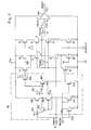
- FIG. 2 shows a general block diagram of an inverter type oscillator circuit constituting a preferred embodiment of the present invention.
- the inverter oscillator circuit 10 illustrated in FIG. 2 typically comprises the parallel arrangement, between input A and output B terminals, of inverting amplifier means comprising first and second inverters 2, 3, of a resonator 1 and a resistor 4, first and second charge capacitors 5, 6 being respectively connected between said input and output terminals A, B, on the one hand, and a supply potential, here V SS , of somewhere else.
- the oscillator circuit 10 may further comprise an additional resistive element 40, of value R O , disposed between the output of the inverters 2, 3, on the one hand, and the resonator 1 as well as the charge capacitor 6, on the other hand .
- This optional resistive element 40 is in particular intended to increase the stability of the oscillator circuit.
- the arrangement of the two inverters 2, 3 is substantially similar to the arrangement illustrated in FIG. 1b, that is to say that the first inverter 2 is permanently connected between the input A and output B terminals, while the second inverter 3 is capable of being connected or disconnected from these terminals A, B under the action of the control circuit 8.
- the second inverter 3 is activated or deactivated using means of switching (namely two switches 7a and 7b controlled by the control circuit 8) placed in the supply path of the inverter, between the supply potentials V DD and V SS .
- the second inverter 3 could alternatively be connected or disconnected from terminals A and B by means of a switch connected in series with this reverser, for example by means of a transmission gate comprising the parallel arrangement of an n-MOS transistor and a p-MOS transistor connected one to each other by their drain and source terminals as this is for example illustrated in Figure 5 of the Japanese document JP 60-64506 cited in the preamble.
- the oscillator circuit 10 further comprises means making it possible to smooth the amplitude of the alternating output signal, designated S OSC , during the switching of the oscillator circuit at the end of the start-up phase.
- S OSC amplitude adjustment loop
- These means for smoothing the amplitude of the output signal are advantageously produced in the form of an amplitude adjustment loop generally designated by the reference numeral 9.
- This amplitude adjustment loop 9 is connected, on the one hand, to one of the input and output terminals A, B of the oscillator circuit 10 (in this example, the input terminal A), and, on the other hand, on the first inverter 2.
- the amplitude adjustment loop 9 comprises on the one hand a regulating circuit amplitude 90 and on the other hand at least one controlled current source 91, 92 (preferably two) connected in the supply path of the inverter 2.
- an input terminal 90a of the amplitude regulator 90 is connected to the terminal input A of the oscillator circuit, and two output terminals 90b, 90c are respectively connected to first and second controlled current sources 91, 92 placed on either side of the inverter 2 in its feed path.
- each controlled current source 91, 92 is also connected in parallel with a resistive element 95, respectively 96. We will come back later on the usefulness of these resistive elements.
- FIG. 3a schematically illustrates the evolution over time of the transconductance value of the oscillator circuit according to the invention.
- the oscillation conditions have also been illustrated in terms of minimum (g m, min ) and maximum (g m, max ) transconductances for the fundamental modes of vibration in bending (at 74 kHz) and in torsion ( 393 kHz) of the resonator taken by way of example in the European patent application EP 1 111 770 A1 mentioned above.
- FIG. 3b schematically illustrates the corresponding evolution of the alternating output signal S OSC of the oscillator.
- the two inverters 2, 3 of the oscillator circuit are connected in parallel so that the circuit has an overall transconductance value, called start-up, designated G m , of value high. It will be noted in this respect that the choice of a high transconductance value during the initial phase makes it possible to reduce the start-up time of the oscillator circuit.
- the starting transconductance value G m of the circuit is selected so that the oscillation conditions of the desired mode (namely the fundamental mode of torsional vibration ) are satisfied. These conditions are satisfied, in the example illustrated, for a starting transconductance value G m comprised between the upper critical value g m, max of the unwanted flexion vibration mode (at 74 kHz) and the higher critical value g m , max of the desired torsional vibration mode (at 393 kHz).
- the resonator is vibrated according to the desired torsional vibration mode.
- the amplitude of the output signal S OSC gradually increases and the frequency of the oscillations tends towards a stable state.
- T STAB a determined time interval
- the second inverter 3 is deactivated so as to reduce the transconductance value of the circuit to a so-called reduced value, designated g m , and thus reduce the consumption of the circuit.
- the reduced transconductance value g m is preferably determined so that it always satisfies the strict oscillation conditions of the desired torsional vibration mode. The inventor has nevertheless observed that the transconductance value can be reduced to a value no longer strictly meeting the above-mentioned oscillation conditions. In the example of FIG.
- the present invention makes it possible to reduce the consumption of the inverter circuit below the consumption level defined by the lower oscillation condition, that is to say the upper critical transconductance value g m, max of the mode undesired bending vibration (this value is typically greater than the lower critical transconductance g m, min of the desired torsional vibration mode).
- the transition from the starting transconductance value G m to the reduced transconductance value g m is not carried out abruptly but gradually thanks to the addition of the amplitude adjustment loop connected to the first oscillator circuit inverter. This results in a smooth and gradual decrease in the amplitude of the output signal S OSC as illustrated in FIG. 3b.
- the consumption of the oscillator circuit can be further reduced by adding a resistive element 95, 96 in the supply path of the first inverter 2 in parallel with each source of controlled current 91, 92.
- the addition of these resistive elements has the effect of limit the maximum current in the supply path of inverter 2 and therefore further reduce the consumption of the inverter oscillator circuit in steady state.
- V R an intermediate supply potential
- FIG. 4 shows a detailed embodiment of the oscillator circuit with inverter of Figure 2.
- the resonator 1 connected between terminals A and B
- the charge capacitors 5 and 6 have not been shown in Figure 4.
- the first and second inverters 2, 3 are CMOS inverters comprising each a p-MOS transistor 21, resp. 31, the drain of which is connected to the drain of a n-MOS transistor 22, resp. 32.
- the gates of the transistors 21, 22, 31 and 32 are connected to the same node and form the input terminal A of the oscillator circuit.
- the drains of the transistors 21, 22, 31, 32 are connected together to the output terminal B, here via the additional resistive element 40.
- the resistive feedback element 4 is connected between the grid connection node and the drain connection node transistors 21, 22, 31, 32.
- the output signal from the oscillator circuit (taken from this example on terminal A) is typically applied to the entry of a floor of formatting 100 making it possible to deliver a square output signal.
- the source of the p-MOS transistor 31 of the second inverter 3 is connected to the high supply potential V DD via another p-MOS transistor forming the switch 7a.
- the source of the n-MOS transistor 32 of the second inverter 3 is connected to the low supply potential (here the intermediate supply potential V R ) via another n-MOS transistor forming the switch. 7b.
- a control signal designated STARTUP is applied to the gate of the n-MOS transistor 7b as well as to the gate of the p-MOS transistor 7a (via an inverter) in order to control their conduction state and selectively activate or deactivate the second inverter 3.
- the source of the p-MOS transistor 21 of the first inverter 2 is connected to the high supply potential V DD by means of another p-MOS transistor connected in resistance configuration (gate potential brought to ground), this p-MOS transistor forming the resistive element 95 of FIG. 2.
- a p-MOS transistor forming the first controlled current source 91 is on the other hand interposed between the source of the p-MOS transistor 21 and the high potential V DD in parallel with the transistor 95 connected in resistance.
- the source of the n-MOS transistor 22 is connected to the low supply potential V R via an n-MOS transistor connected in resistance configuration (potential of the gate brought to the high potential) and forming l resistive element 96 of FIG. 2.
- An n-MOS transistor forming the second controlled current source 92 is interposed between the source of the n-MOS transistor 22 and the low potential V R in parallel with the transistor 96 connected in resistance.
- the p-MOS 91 and n-MOS 92 transistors forming the current sources controlled are controlled by the amplitude regulator circuit 90 which is going now briefly describe the structure. Note that a person skilled in the art can consider other configurations for the realization of this regulator circuit amplitude and that the configuration illustrated cannot therefore be considered a limitation of the invention.
- the input terminal A of the oscillator circuit is applied to a terminal of a first capacitive element 921, the other terminal of this capacitive element 921 being connected on the one hand to the drain of a first p-MOS transistor 901 and, on the other hand, to the gate of a second p-MOS transistor 902.
- the source of the latter is connected to the high potential V DD while its drain is connected to the source of the first p-MOS transistor 901 as well as the source of a third p-MOS transistor 903.
- the gate and the drain of this third p-MOS transistor 903 are connected to the gate of the first transistor 901.
- connection node between the drain of the p-MOS transistor 902 and the sources of the p-MOS transistors 901 and 903 is connected to the gate of a fourth p-MOS transistor 904 whose source is connected to the high potential V DD .
- Second 922 and third 923 capacitive elements are moreover connected by one of their terminals respectively to the drain of the p-MOS transistor 902 and to the drain of the p-MOS transistor 903, the other terminal of these capacitive elements 922 and 923 being connected to the high supply potential V DD .
- the gate of the p-MOS transistor forming the first controlled current source 91 is connected to the gate of the fourth p-MOS transistor 904, a fifth p-MOS transistor 905 connected in capacitance configuration (drain and source terminals connected to the potential top V DD ) being connected by its gate on this same connection between the p-MOS transistors 91 and 904.
- the gate of the n-MOS transistor forming the second controlled current source 92 is in turn connected to the drain of the fourth transistor p- MOS 904.
- the polarization of the transistors of the amplitude regulator circuit 90 is ensured by an IBPOSC bias current which is mirrored in the branch comprising the p-MOS 903 transistor and in the branch comprising the p-MOS 904 transistor at by means of a current mirror comprising three n-MOS transistors 910, 911 and 912, the transistors 911 and 912 of the first and second output branches of the mirror current being respectively connected in series with the p-MOS transistor 903 and the p-MOS 904 transistor.
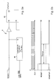
- FIG. 5a shows an exemplary embodiment of the control circuit 8 used to generate the STARTUP control signal intended for switches 7a and 7b.
- This control circuit 8 produced in digital form, comprises essentially a flip-flop S-R 80 and a counter, or divider, 85.
- the counter 85 is clocked by a clock signal CLK (purely as an example Illustrative and not limiting, a clock signal at 128 Hz derived from the output signal of the oscillator circuit).
- a RESET reset signal is applied to a terminal resetting of the counter 85 as well as on the excitation terminal S of the flip-flop 80, via an inverter.
- the switching signal STARTUP thus passes to the high logic level during a determined time interval of duration T STAB .
- the oscillator circuit of FIG. 2 is therefore switched to the "high transconductance" mode favoring the rapid start of the oscillations.
- the STARTUP signal goes to the low logic level, thus switching the oscillator circuit of FIG. 2 to the "low transconductance” mode thus reducing the consumption of the circuit.
Landscapes
- Oscillators With Electromechanical Resonators (AREA)
- Logic Circuits (AREA)
Abstract
Description
La présente invention concerne de manière générale un circuit oscillateur à inverseur à consommation réduite. Plus particulièrement, la présente invention concerne un circuit oscillateur à inverseur à relativement basse fréquence comportant préférablement un résonateur à quartz agencé pour vibrer selon un mode de vibration en torsion.The present invention relates generally to an oscillator circuit with inverter with reduced consumption. More particularly, the present invention relates to a relatively low frequency inverter oscillator circuit comprising preferably a quartz resonator arranged to vibrate according to a vibration mode in torsion.
On connaít déjà de la demande de brevet européen EP 1 111 770 A1, au nom
de Eta SA Fabriques d'Ebauches et EM Microelectronic-Marin SA, un dispositif
oscillateur à quartz basse fréquence ayant un comportement thermique amélioré.
Cette demande, incorporée ici par référence, décrit un circuit oscillateur de type à
inverseur comportant un résonateur à quartz spécifique agencé pour vibrer selon un
mode de vibration en torsion. Ce résonateur spécifique, qui est décrit dans l'article de
MM. Roger Bourquin et Philippe Truchot, « Barreau de quartz vibrant en mode de
torsion, Application aux capteurs », 6ème Congrès Européen de Chronométrie (CEC),
Bienne, 17-18 octobre 1996 (cité et incorporé par référence dans la demande de
brevet européen susmentionnée), présente un unique angle de coupe défini par une
rotation autour de l'axe cristallographique X du cristal de quartz, et comporte en
particulier un mode fondamental de vibration en flexion non désiré se situant à une
première fréquence et un mode fondamental de vibration en torsion désiré se situant
à une deuxième fréquence supérieure à la première fréquence du mode fondamental
de vibration en flexion non désiré.We already know from European
Le circuit d'entretien des oscillations du résonateur est du type à inverseur. Afin d'assurer que le résonateur vibre selon le mode fondamental de vibration en torsion désiré, et non selon le mode fondamental de vibration en flexion non désiré, le circuit inverseur est conçu pour présenter une valeur de transconductance telle que les conditions limites de vibration (ou valeurs de transconductance critiques minimale et maximale) soient satisfaites pour le mode fondamental de vibration en torsion et non pour le mode fondamental de vibration en flexion.The resonator oscillation maintenance circuit is of the inverter type. In order to ensure that the resonator vibrates according to the fundamental mode of vibration in desired torsion, and not according to the fundamental mode of vibration in unwanted bending, the inverter circuit is designed to have a transconductance value such that vibration boundary conditions (or minimum critical transconductance values and maximum) are satisfied for the fundamental mode of vibration in torsion and not for the fundamental mode of vibration in bending.
Le comportement thermique du dispositif oscillateur ainsi conçu est ainsi grandement amélioré par rapport aux dispositifs oscillateurs conventionnels et présente notamment un comportement thermique similaire aux circuits employant des résonateurs dits de coupe AT pour une fréquence de fonctionnement nettement moins élevée (typiquement de 393 kHz pour le résonateur torsion comparé aux 4 MHz du résonateur de coupe AT) et donc une consommation comparativement inférieure.The thermal behavior of the oscillator device thus designed is thus greatly improved compared to conventional oscillating devices and exhibits in particular a thermal behavior similar to circuits employing so-called AT cut resonators for a clearly operating frequency lower (typically 393 kHz for the torsion resonator compared to 4 MHz of the cut resonator AT) and therefore a comparatively lower consumption.
Abstraction faite des avantages en terme de stabilité thermique, la consommation du circuit oscillateur décrit dans la demande européenne susmentionnée reste néanmoins comparativement plus élevée que celle des circuits oscillateurs basse fréquence conventionnels. La présente invention a donc pour but principal de proposer un circuit oscillateur de type à inverseur présentant une consommation plus réduite, ce circuit oscillateur comportant préférablement, mais pas nécessairement, un résonateur vibrant en torsion du type susmentionné.Leaving aside the advantages in terms of thermal stability, the consumption of the oscillator circuit described in the European application aforementioned remains nevertheless comparatively higher than that of the circuits conventional low frequency oscillators. The object of the present invention is therefore main to propose an inverter type oscillator circuit having a lower consumption, this oscillator circuit preferably comprising, but not necessarily, a torsional vibrating resonator of the aforementioned type.
On notera que l'on connaít déjà une solution permettant de réduire la
consommation d'un circuit oscillateur à inverseur de la demande de brevet
JP 60-64506 au nom de la société Fujitsu Ltd., déposée le 20 septembre 1983. Les
figures 1a et 1b montrent deux schémas de principe de ce circuit oscillateur à
inverseur, indiqué globalement par la référence numérique 10. Globalement, chacun
des circuits oscillateurs illustrés correspond à un circuit oscillateur à inverseur
classique comportant notamment l'agencement parallèle, entre des bornes d'entrée A
et de sortie B, d'un moyen amplificateur inverseur 2, 3, d'un résonateur 1 et d'un
élément résistif 4, dit résistance de contre-réaction, de valeur RF. Des premier et
second condensateurs de charge 5, 6 sont respectivement connectés entre les
bornes d'entrée A et de sortie B, d'une part, et un potentiel d'alimentation, ici VSS,
d'autre part.Note that we already know a solution to reduce the consumption of an inverter oscillator circuit of patent application JP 60-64506 in the name of the company Fujitsu Ltd., filed September 20, 1983. Figures 1a and 1b show two block diagrams of this inverter oscillator circuit, indicated overall by the
Ce circuit oscillateur 10 comporte en outre des moyens de commande 8 et un
moyen de commutation 7 pour commander le moyen amplificateur inverseur 2, 3 de
sorte qu'il présente une première valeur de transconductance durant une phase de
démarrage et une seconde valeur de transconductance inférieure à la première valeur
de transconductance en régime établi au terme de la phase de démarrage.This
Plus précisément, le circuit oscillateur 10 de la figure 1a comprend un premier
inverseur 2 ayant une première valeur de transconductance, désignée gm, et un
second inverseur 3 ayant une seconde valeur de transconductance, désignée Gm,
supérieure à la première valeur de transconductance gm. Le moyen de commutation 7
est disposé de manière à sélectivement connecter le premier inverseur 2 ou le second
inverseur 3 entre les bornes d'entrée et de sortie A, B. Durant la phase de démarrage,
le moyen de commutation 7 est en position « 1» de manière à connecter le second
inverseur entre les bornes A et B. Dès lors que les oscillations sont stables, en régime
dit établi, le moyen de commutation 7 passe en position « 2 » sous l'action des
moyens de commande 8.More specifically, the
Le circuit oscillateur 10 de la figure 1b est sensiblement similaire au circuit de
la figure 1a. Le second inverseur 3 présente ici uniquement une valeur de
transconductance additionnelle ou complémentaire, désignée Δgm, qui est ajoutée à
la valeur de transconductance gm du premier inverseur 2 lors de la phase de
démarrage. Le moyen de commutation 7 est ainsi connecté de sorte que le second
inverseur 3 est connecté en parallèle avec le premier inverseur 2 lors de la phase de
démarrage (moyen de commutation 7 en position « 1 ») et déconnecté de ce second
inverseur 2 en régime établi (moyen de commutation 7 en position « 2 »).The
On notera que l'utilisation des solutions proposées dans le document japonais susmentionné peut avoir plusieurs inconvénients. En particulier, la diminution de la valeur de transconductance lors de la commutation au terme de la phase de démarrage a pour conséquence une diminution du courant (et donc de la consommation) qui se traduit également par une brusque diminution de l'amplitude du signal de sortie de l'oscillateur. Cette commutation du circuit oscillateur peut en particulier conduire à un fort amortissement des vibrations du résonateur qui peut éventuellement conduire à son arrêt total ou à une modification de son mode de vibration. En particulier, l'inventeur a pu constater que si la solution proposée dans le document japonais susmentionné était directement associée au résonateur susmentionné agencé pour vibrer en torsion, celle-ci conduisait soit à l'arrêt total du résonateur ou à une modification de son mode de vibration vers le mode fondamental de vibration en flexion non désiré.Note that the use of the solutions proposed in the Japanese document the above can have several disadvantages. In particular, the decrease in transconductance value when switching at the end of the starting results in a reduction in the current (and therefore in the consumption) which also results in a sudden decrease in the amplitude of the oscillator output signal. This switching of the oscillator circuit can particular lead to a strong damping of the vibrations of the resonator which can possibly lead to its total stop or to a modification of its mode of vibration. In particular, the inventor was able to observe that if the solution proposed in the aforementioned Japanese document was directly associated with the resonator aforementioned arranged to vibrate in torsion, this led either to the complete stop of the resonator or a change in its vibration mode to the fundamental mode unwanted flexural vibration.
On notera en outre que la diminution brusque de l'amplitude du signal de sortie de l'oscillateur peut également être un inconvénient pour les éléments périphériques associés au circuit oscillateur.It should also be noted that the sudden decrease in the amplitude of the output signal of the oscillator can also be a disadvantage for the peripheral elements associated with the oscillator circuit.
L'utilisation du principe énoncé dans la demande de brevet japonais
susmentionnée, en particulier en association avec le circuit oscillateur de la demande
de brevet européen EP 1 111 770 A1 mentionnée en préambule, requiert ainsi une
attention toute particulière étant donné les conditions spécifiques auxquelles doit
satisfaire le circuit oscillateur pour que le résonateur vibre selon le mode de vibration
désiré.Use of the principle stated in the Japanese patent application
mentioned above, in particular in association with the demand oscillator circuit
of
Un autre but de la présente invention est donc de proposer un circuit oscillateur à consommation réduite qui soit aisément intégrable dans un système global, qui n'engendre pas de perturbations sur ce système et qui assure un maintien adéquat des vibrations du résonateur. En particulier, dans le cas où le circuit oscillateur emploie un résonateur à quartz vibrant en torsion du type susmentionné, on désire une solution garantissant que le mode de vibration en torsion est maintenu en sus de la réduction de consommation.Another object of the present invention is therefore to propose a circuit low consumption oscillator which can be easily integrated into a system global, which does not cause disturbances on this system and which ensures maintenance adequate vibrations of the resonator. In particular, in the case where the circuit oscillator employs a torsional vibrating quartz resonator of the aforementioned type, we want a solution guaranteeing that the torsional vibration mode is maintained in addition to the reduction in consumption.
Encore un autre but de la présente invention et de pousser encore plus loin la réduction de consommation du circuit et de proposer une solution qui soit encore moins gourmande en énergie.Yet another object of the present invention and to push the reduction of circuit consumption and to propose a solution which is still less energy intensive.
La présente invention a également pour but de proposer un procédé d'entretien des oscillations d'un résonateur du type susmentionné garantissant, d'une part, une réduction de la consommation, et, d'autre part, le maintien des oscillations du résonateur selon le mode fondamental de vibration en torsion désiré.The present invention also aims to provide a method maintenance of the oscillations of a resonator of the aforementioned type ensuring, of a on the one hand, a reduction in consumption, and, on the other hand, the maintenance of oscillations of the resonator according to the fundamental mode of vibration in torsion desired.
La présente invention a donc pour objet un circuit oscillateur à inverseur dont
les caractéristiques sont énoncées dans la revendication indépendante 1.The present invention therefore relates to an inverter oscillator circuit of which
the features are set out in
La présente invention a également pour objet un procédé d'entretien des oscillations d'un résonateur du type susmentionné dont les caractéristiques sont énoncées dans la revendication indépendante 13.The present invention also relates to a method for maintaining the oscillations of a resonator of the aforementioned type whose characteristics are set out in independent claim 13.
Des modes de réalisation avantageux de la présente invention font l'objet des revendications indépendantes.Advantageous embodiments of the present invention are the subject of independent claims.
En se référant à la demande de brevet européen EP 1 111 770 A1
susmentionnée, on notera au sujet du résonateur spécifique agencé pour vibrer selon
un mode de vibration en torsion que le circuit entretenant les vibrations du résonateur
est agencé pour forcer le résonateur à vibrer selon le mode de vibration en torsion
désiré et que, pour ce faire, la valeur de transconductance de l'inverseur est choisie
supérieure à la valeur de transconductance maximale, désignée gm,max, associée au
mode de vibration en flexion non désiré. La transconductance étant notamment
représentative du courant consommé par le circuit, on comprendra donc que le circuit
consomme plus lorsque celui-ci est agencé pour forcer le résonateur à vibrer selon le
mode de vibration en torsion que lorsque ce même circuit est agencé pour vibrer
selon le mode de vibration en flexion classique.Referring to the above-mentioned European
Toutefois, selon la présente invention, l'inventeur a pu constater que la consommation du circuit peut être réduite une fois que le circuit oscillateur est démarré et que son signal de sortie est stable. En particulier, il est possible de faire démarrer le circuit pour que le résonateur vibre selon le mode de torsion désiré en satisfaisant les contraintes strictes déterminées par les valeurs de transconductances critiques définies dans la demande de brevet européen susmentionnée, et, au terme de cette phase de démarrage, réduire la consommation en garantissant que le résonateur vibre toujours selon ce mode de vibration en torsion. Cette réduction de la consommation est en partie obtenue en commutant le circuit, durant la phase dite de régime établi suivant la phase de démarrage, dans un autre état où celui-ci présente une valeur de transconductance réduite par rapport à la valeur de transconductance initiale définie pour le démarrage.However, according to the present invention, the inventor has found that the circuit consumption can be reduced once the oscillator circuit is started and its output signal is stable. In particular, it is possible to do start the circuit so that the resonator vibrates according to the desired torsion mode while satisfying the strict constraints determined by the transconductance values criticisms defined in the aforementioned European patent application, and, at the end reduce the consumption by ensuring that the resonator always vibrates according to this torsional vibration mode. This reduction in consumption is partly obtained by switching the circuit, during the so-called regime established following the start-up phase, in another state where this presents a reduced transconductance value compared to the transconductance value initial defined for startup.
Avantageusement, l'inventeur a pu constater que la valeur de transconductance de l'inverseur peut éventuellement être réduite à une valeur inférieure à la valeur de transconductance critique en-dessous de laquelle les oscillations du résonateur selon le mode de vibration en torsion ne sont normalement plus garantie. L'inventeur a ainsi constaté que les valeurs de transconductances critiques sont essentiellement déterminantes lors de la phase de démarrage du résonateur. Par souci de sécurité, il est néanmoins parfaitement envisageable de garder la valeur de transconductance du circuit dans la gamme de valeurs évitant que le résonateur vibre selon le mode de vibration en torsion.Advantageously, the inventor was able to observe that the value of transconductance of the inverter can possibly be reduced to a value lower than the critical transconductance value below which the oscillations of the resonator according to the torsional vibration mode are not normally more guaranteed. The inventor thus found that the values of transconductances critics are essentially decisive during the start-up phase of the resonator. For security reasons, it is nevertheless perfectly possible to keep the transconductance value of the circuit in the range of values avoiding that the resonator vibrates according to the torsional vibration mode.
Outre la réduction de la consommation en régime établi, la présente invention assure également un démarrage rapide du circuit oscillateur par le choix d'une valeur de transconductance élevée durant cette phase initiale.In addition to reducing consumption in steady state, the present invention also ensures rapid start-up of the oscillator circuit by choosing a value high transconductance during this initial phase.
Selon l'invention, le circuit oscillateur est en outre équipé de moyens permettant de lisser l'amplitude de sortie du signal alternatif lors du passage de la phase de démarrage en régime établi, c'est-à-dire lors de la réduction de la valeur de transconductance du circuit. Ce lissage de l'amplitude du signal de sortie permet de limiter les effets de la commutation de la valeur de transconductance du circuit oscillateur et de garantir que les vibrations du résonateur ne soient pas amorties trop brusquement afin d'assurer que le résonateur continue à vibrer selon son mode de vibration désiré. D'autre part, ce lissage favorise l'intégration du circuit oscillateur dans un système global, les perturbations causées par la commutation du circuit oscillateur d'un état à l'autre étant minimisées.According to the invention, the oscillator circuit is further equipped with means allowing to smooth the amplitude of output of the alternating signal during the passage of the start-up phase in steady state, i.e. when the value of transconductance of the circuit. This smoothing of the amplitude of the output signal allows limit the effects of switching the transconductance value of the circuit oscillator and ensure that the vibrations of the resonator are not dampened too much suddenly to ensure that the resonator continues to vibrate according to its mode of desired vibration. On the other hand, this smoothing promotes the integration of the oscillator circuit in a global system, disturbances caused by circuit switching oscillator from one state to another being minimized.
Selon d'autres modes de réalisation de la présente invention, des moyens complémentaires sont utilisés pour réduire la consommation du circuit oscillateur en régime établi. Selon un premier de ces modes de réalisation, des éléments résistifs sont connectés en série dans le chemin d'alimentation du circuit inverseur. Selon un autre de ces modes de réalisation de l'invention, le circuit comporte en outre un régulateur de tension permettant d'abaisser la tension d'alimentation du circuit inverseur.According to other embodiments of the present invention, means are used to reduce the consumption of the oscillator circuit by established regime. According to a first of these embodiments, resistive elements are connected in series in the supply path of the inverter circuit. According to a other of these embodiments of the invention, the circuit further comprises a voltage regulator to lower the circuit supply voltage inverter.
D'autres caractéristiques et avantages de la présente invention apparaítront plus clairement à la lecture de la description détaillée qui suit, faite en référence aux dessins annexés donnés à titre d'exemples non limitatifs et dans lesquels :
- les figures 1a et 1b, déjà présentées, montrent deux schémas de principe d'un circuit oscillateur à inverseur décrit dans le document JP 60-64506 susmentionné ;
- la figure 2, montre un schéma général du circuit oscillateur à inverseur selon la présent invention ;
- la figure 3a illustre l'évolution au cours du temps de la valeur de transconductance du circuit oscillateur à inverseur de la figure 2, notamment durant la commutation d'une phase de démarrage vers une phase de régime établi ;
- la figure 3b illustre l'évolution au cours du temps de l'amplitude du signal d'oscillation délivré par le circuit oscillateur de la figure 2, notamment durant la commutation d'une phase de démarrage vers une phase de régime établi ;
- la figure 4 est un exemple détaillé d'un mode de réalisation du circuit oscillateur selon l'invention ;
- la figure 5a est un exemple de réalisation d'un circuit de génération d'un signal de commutation STARTUP permettant de commuter le circuit oscillateur de la figure 2 de la phase de démarrage à la phase de régime établi ; et
- la figure 5b est un diagramme illustrant l'évolution au cours du temps des signaux du circuit générateur de la figure 5a.
- Figures 1a and 1b, already presented, show two block diagrams of an inverter oscillator circuit described in the document JP 60-64506 mentioned above;
- Figure 2 shows a general diagram of the inverter oscillator circuit according to the present invention;
- FIG. 3a illustrates the evolution over time of the transconductance value of the inverter oscillator circuit of FIG. 2, in particular during the switching from a start-up phase to a steady state phase;
- FIG. 3b illustrates the evolution over time of the amplitude of the oscillation signal delivered by the oscillator circuit of FIG. 2, in particular during the switching from a start-up phase to a steady state phase;
- FIG. 4 is a detailed example of an embodiment of the oscillator circuit according to the invention;
- FIG. 5a is an exemplary embodiment of a circuit for generating a STARTUP switching signal making it possible to switch the oscillator circuit of FIG. 2 from the start-up phase to the steady state phase; and
- FIG. 5b is a diagram illustrating the evolution over time of the signals of the generator circuit of FIG. 5a.
La figure 2 montre un schéma de principe général d'un circuit oscillateur de
type à inverseur constituant un mode de réalisation préféré de la présente invention.
Le circuit oscillateur à inverseur 10 illustré dans la figure 2 comprend typiquement
l'agencement parallèle, entre des bornes d'entrée A et de sortie B, de moyens
amplificateur inverseur comprenant des premier et second inverseurs 2, 3, d'un
résonateur 1 et d'une résistance 4, des premier et second condensateurs de charge
5, 6 étant respectivement connectés entre lesdites bornes d'entrée et de sortie A, B,
d'une part, et un potentiel d'alimentation, ici VSS, d'autre part. Le circuit oscillateur 10
peut en outre comprendre un élément résistif additionnel 40, de valeur RO, disposé
entre la sortie des inverseurs 2, 3, d'une part, et le résonateur 1 ainsi que le
condensateur de charge 6, d'autre part. Cet élément résistif optionnel 40 est
notamment destiné à augmenter la stabilité du circuit oscillateur.Figure 2 shows a general block diagram of an inverter type oscillator circuit constituting a preferred embodiment of the present invention. The
L'agencement des deux inverseurs 2, 3 est sensiblement analogue à
l'agencement illustré dans la figure 1b, c'est-à-dire que le premier inverseur 2 est
connecté en permanence entre les bornes d'entrée A et de sortie B, alors que le
second inverseur 3 est susceptible d'être connecté ou déconnecté de ces bornes A, B
sous l'action du circuit de commande 8. En l'occurrence, le second inverseur 3 est
activé ou désactivé à l'aide de moyens de commutation (à savoir deux interrupteurs
7a et 7b contrôlés par le circuit de commande 8) placés dans le chemin d'alimentation
de l'inverseur, entre les potentiels d'alimentation VDD et VSS.The arrangement of the two
On notera que le second inverseur 3 pourrait alternativement être connecté ou
déconnecté des bornes A et B au moyen d'un interrupteur connecté en série avec cet
inverseur, par exemple au moyen d'une porte de transmission comprenant
l'agencement parallèle d'un transistor n-MOS et d'un transistor p-MOS connectés l'un
à l'autre par leurs terminaux de drain et de source comme cela est par exemple
illustré dans la figure 5 du document japonais JP 60-64506 cité en préambule.Note that the
Le circuit oscillateur 10 comprend en outre des moyens permettant de lisser
l'amplitude du signal de sortie alternatif, désigné SOSC, lors de la commutation du
circuit oscillateur au terme de la phase de démarrage. Ces moyens de lissage de
l'amplitude du signal de sortie sont avantageusement réalisés sous la forme d'une
boucle de réglage en amplitude désignée globalement par la référence numérique 9.
Cette boucle de réglage en amplitude 9 est connectée, d'une part, sur l'une des
bornes d'entrée et de sortie A, B du circuit oscillateur 10 (dans cet exemple, la borne
d'entrée A), et, d'autre part, sur le premier inverseur 2.The
La boucle de réglage en amplitude 9 comprend d'une part un circuit régulateur
d'amplitude 90 et d'autre part au moins une source de courant contrôlée 91, 92
(préférablement deux) connectée dans le chemin d'alimentation de l'inverseur 2. Dans
cet exemple, une borne d'entrée 90a du régulateur d'amplitude 90 est relié à la borne
d'entrée A du circuit oscillateur, et deux bornes de sorties 90b, 90c sont
respectivement connectées à des première et seconde sources de courant contrôlées
91, 92 placées de part et d'autre de l'inverseur 2 dans son chemin d'alimentation. Au
titre de première amélioration, chaque source de courant contrôlée 91, 92 est en outre
connectée en parallèle avec un élément résistif 95, respectivement 96. On reviendra
ultérieurement sur l'utilité de ces éléments résistifs.The
En se référant aux figures 3a et 3b, on va maintenant brièvement décrire le
principe de fonctionnement du circuit oscillateur à inverseur selon la présente
invention. La figure 3a illustre schématiquement l'évolution au cours du temps de la
valeur de transconductance du circuit oscillateur selon l'invention. Dans la figure 3a,
on a également illustré les conditions d'oscillation en termes de transconductances
minimales (gm,min) et maximales (gm,max) pour les modes fondamentaux de vibration
en flexion (à 74 kHz) et en torsion (393 kHz) du résonateur pris à titre d'exemple dans
la demande de brevet européen EP 1 111 770 A1 susmentionnée. La figure 3b illustre
schématiquement l'évolution correspondante du signal de sortie alternatif SOSC de
l'oscillateur.Referring to Figures 3a and 3b, we will now briefly describe the operating principle of the inverter oscillator circuit according to the present invention. FIG. 3a schematically illustrates the evolution over time of the transconductance value of the oscillator circuit according to the invention. In FIG. 3a, the oscillation conditions have also been illustrated in terms of minimum (g m, min ) and maximum (g m, max ) transconductances for the fundamental modes of vibration in bending (at 74 kHz) and in torsion ( 393 kHz) of the resonator taken by way of example in the European
Durant la phase de démarrage du circuit oscillateur (phase « 1 »), les deux
inverseurs 2, 3 du circuit oscillateur sont connectés en parallèle de sorte que le circuit
présente une valeur de transconductance globale, dite de démarrage, désignée Gm,
de valeur élevée. On notera à ce titre que le choix d'une valeur de transconductance
élevée durant la phase initiale permet de réduire le temps de démarrage du circuit
oscillateur.During the start-up phase of the oscillator circuit (phase "1"), the two
Afin de mettre le résonateur en vibration selon le mode fondamental de vibration en torsion désiré, la valeur de transconductance de démarrage Gm du circuit est sélectionnée de sorte que les conditions d'oscillations du mode désirés (à savoir le mode fondamental de vibration en torsion) soient satisfaites. Ces conditions sont satisfaites, dans l'exemple illustré, pour une valeur de transconductance de démarrage Gm comprise entre la valeur critique supérieure gm,max du mode de vibration en flexion non désiré (à 74 kHz) et la valeur critique supérieure gm,max du mode de vibration en torsion désiré (à 393 kHz).In order to set the resonator in vibration according to the fundamental mode of torsional vibration, the starting transconductance value G m of the circuit is selected so that the oscillation conditions of the desired mode (namely the fundamental mode of torsional vibration ) are satisfied. These conditions are satisfied, in the example illustrated, for a starting transconductance value G m comprised between the upper critical value g m, max of the unwanted flexion vibration mode (at 74 kHz) and the higher critical value g m , max of the desired torsional vibration mode (at 393 kHz).
En satisfaisant les conditions susmentionnées, le résonateur est mis en vibration selon le mode de vibration en torsion désiré. Comme illustré dans la figure 3b, l'amplitude du signal de sortie SOSC augmente graduellement et la fréquence des oscillations tend vers un état stable. Par convention, on dira que les oscillations sont stabilisées au terme d'un intervalle de temps déterminé, désigné TSTAB.By satisfying the above conditions, the resonator is vibrated according to the desired torsional vibration mode. As illustrated in FIG. 3b, the amplitude of the output signal S OSC gradually increases and the frequency of the oscillations tends towards a stable state. By convention, we will say that the oscillations are stabilized at the end of a determined time interval, designated T STAB .
Au terme de la phase de démarrage, dès lors que les oscillations du circuit
oscillateur sont stabilisées (en régime dit établi, phase « 2 » dans les figures), le
second inverseur 3 est désactivé de manière à réduire la valeur de transconductance
du circuit à une valeur dite réduite, désignée gm, et ainsi réduire la consommation du
circuit. Par souci de sécurité, la valeur de transconductance réduite gm est
préférablement déterminée de sorte qu'elle satisfait toujours aux conditions
d'oscillation strictes du mode de vibration en torsion désiré. L'inventeur a néanmoins
pu constater que la valeur de transconductance peut être réduite à une valeur ne
satisfaisant plus strictement les conditions d'oscillations susmentionnées. Dans
l'exemple de la figure 3a, il est par exemple possible de réduire la valeur de
transconductance du circuit à une valeur comprise entre la transconductance critique
supérieure gm,max du mode de vibration en flexion non désiré et la transconductance
critique inférieure gm,min du mode de vibration en torsion désiré, cette possibilité étant
illustrée dans la figure 3a par la courbe en traits interrompus. On comprendra donc
que la présente invention permet de réduire la consommation du circuit inverseur en-deçà
du niveau de consommation défini par la condition d'oscillation inférieure, c'est-à-dire
la valeur de transconductance critique supérieure gm,max du mode de vibration
en flexion non désiré (cette valeur étant typiquement supérieure à la
transconductance critique inférieure gm,min du mode de vibration en torsion désiré).At the end of the start-up phase, as soon as the oscillations of the oscillator circuit are stabilized (in so-called steady state, phase "2" in the figures), the
Selon la présente invention, la transition de la valeur de transconductance de démarrage Gm à la valeur de transconductance réduite gm n'est pas opérée de manière abrupte mais graduelle grâce à l'adjonction de la boucle de réglage en amplitude connectée sur le premier inverseur du circuit oscillateur. Il en résulte une diminution douce et progressive de l'amplitude du signal de sortie SOSC comme illustré dans la figure 3b.According to the present invention, the transition from the starting transconductance value G m to the reduced transconductance value g m is not carried out abruptly but gradually thanks to the addition of the amplitude adjustment loop connected to the first oscillator circuit inverter. This results in a smooth and gradual decrease in the amplitude of the output signal S OSC as illustrated in FIG. 3b.
En se référant à nouveau à la figure 2, on notera que la consommation du
circuit oscillateur peut encore être réduite par l'adjonction d'un élément résistif 95, 96
dans le chemin d'alimentation du premier inverseur 2 en parallèle avec chaque source
de courant contrôlée 91, 92. L'adjonction de ces éléments résistifs a pour effet de
limiter le courant maximum dans le chemin d'alimentation de l'inverseur 2 et donc de
réduire encore la consommation du circuit oscillateur inverseur en régime établi.Referring again to FIG. 2, it will be noted that the consumption of the
oscillator circuit can be further reduced by adding a
Encore au titre d'amélioration, il est possible de réduire la tension d'alimentation aux bornes du circuit oscillateur inverseur, c'est-à-dire produire un potentiel d'alimentation intermédiaire, désigné VR, compris entre les potentiels d'alimentation VDD et VSS.Also as an improvement, it is possible to reduce the supply voltage across the reversing oscillator circuit, that is to say produce an intermediate supply potential, designated V R , between the supply potentials V DD and V SS .
La figure 4 montre une réalisation détaillée du circuit oscillateur à inverseur de
la figure 2. Par souci de clarté, le résonateur 1 (connecté entre les bornes A et B)
ainsi que les condensateurs de charges 5 et 6 (respectivement connectés sur les
bornes A et B) n'ont pas été représentés dans la figure 4.FIG. 4 shows a detailed embodiment of the oscillator circuit with inverter of
Figure 2. For clarity, the resonator 1 (connected between terminals A and B)
as well as the
Les premier et second inverseurs 2, 3 sont des inverseurs CMOS comprenant
chacun un transistor p-MOS 21, resp. 31, dont le drain est connecté au drain d'un
transistor n-MOS 22, resp. 32. Les grilles des transistors 21, 22, 31 et 32 sont
connectées au même noeud et forment la borne d'entrée A du circuit oscillateur. Les
drains des transistors 21, 22, 31, 32 sont connectés ensemble à la borne de sortie B,
ici via l'élément résistif additionnel 40. L'élément résistif de contre-réaction 4 est
connecté entre le noeud de connexion des grilles et le noeud de connexion des drains
des transistors 21, 22, 31, 32. Le signal de sortie du circuit oscillateur (prélevé dans
cet exemple sur la borne A) est appliqué de manière typique à l'entrée d'un étage de
mise en forme 100 permettant de délivrer un signal de sortie carré.The first and
La source du transistor p-MOS 31 du second inverseur 3 est connectée au
potentiel d'alimentation haut VDD par l'intermédiaire d'un autre transistor p-MOS
formant l'interrupteur 7a. De même, la source du transistor n-MOS 32 du second
inverseur 3 est connectée au potentiel d'alimentation bas (ici le potentiel
d'alimentation intermédiaire VR) par l'intermédiaire d'un autre transistor n-MOS
formant l'interrupteur 7b. Un signal de commande désigné STARTUP est appliqué sur
la grille du transistor n-MOS 7b ainsi que sur la grille du transistor p-MOS 7a (via un
inverseur) afin de commander leur état de conduction et sélectivement activer ou
désactiver le second inverseur 3.The source of the p-
La source du transistor p-MOS 21 du premier inverseur 2 est connectée au
potentiel d'alimentation haut VDD par l'intermédiaire d'un autre transistor p-MOS
branché en configuration de résistance (potentiel de la grille amené à la masse), ce
transistor p-MOS formant l'élément résistif 95 de la figure 2. Un transistor p-MOS
formant la première source de courant contrôlée 91 est d'autre part interposé entre la
source du transistor p-MOS 21 et le potentiel haut VDD en parallèle avec le transistor
95 branché en résistance. De même, la source du transistor n-MOS 22 est connectée
au potentiel d'alimentation bas VR par l'intermédiaire d'un transistor n-MOS branché
en configuration de résistance (potentiel de la grille amenée au potentiel haut) et
formant l'élément résistif 96 de la figure 2. Un transistor n-MOS formant la seconde
source de courant contrôlée 92 est interposé entre la source du transistor n-MOS 22
et le potentiel bas VR en parallèle avec le transistor 96 branché en résistance.The source of the p-
Les transistors p-MOS 91 et n-MOS 92 formant les sources de courant
contrôlées sont commandés par le circuit régulateur d'amplitude 90 dont on va
maintenant brièvement décrire la structure. On notera que l'homme du métier pourra
envisager d'autres configurations pour la réalisation de ce circuit régulateur
d'amplitude et que la configuration illustrée ne saurait en conséquence être
considérée comme une limitation de l'invention.The p-
La borne d'entrée A du circuit oscillateur est appliquée sur un terminal d'un
premier élément capacitif 921, l'autre terminal de cet élément capacitif 921 étant
connecté d'une part au drain d'un premier transistor p-MOS 901 et, d'autre part, à la
grille d'un second transistor p-MOS 902. La source de ce dernier est connectée au
potentiel haut VDD alors que son drain est connecté à la source du premier transistor
p-MOS 901 ainsi qu'à la source d'un troisième transistor p-MOS 903. La grille ainsi
que le drain de ce troisième transistor p-MOS 903 sont connectés à la grille du
premier transistor 901. Le noeud de connexion entre le drain du transistor p-MOS 902
et les sources des transistors p-MOS 901 et 903 est relié à la grille d'un quatrième
transistor p-MOS 904 dont la source est connectée au potentiel haut VDD. Des second
922 et troisième 923 éléments capacitifs sont par ailleurs connectés par l'un de leurs
terminaux respectivement sur le drain du transistor p-MOS 902 et sur le drain du
transistor p-MOS 903, l'autre terminal de ces éléments capacitifs 922 et 923 étant
connecté au potentiel d'alimentation haut VDD.The input terminal A of the oscillator circuit is applied to a terminal of a first
La grille du transistor p-MOS formant la première source de courant contrôlée
91 est reliée à la grille du quatrième transistor p-MOS 904, un cinquième transistor p-MOS
905 branché en configuration de capacité (terminaux de drain et de source
connectés au potentiel haut VDD) étant connecté par sa grille sur cette même
connexion entre les transistors p-MOS 91 et 904. La grille du transistor n-MOS
formant la seconde source de courant contrôlée 92 est quant à elle reliée au drain du
quatrième transistor p-MOS 904.The gate of the p-MOS transistor forming the first controlled
La polarisation des transistors du circuit régulateur d'amplitude 90 est assurée
par un courant de polarisation IBPOSC qui est miroité dans la branche comportant le
transistor p-MOS 903 et dans la branche comportant le transistor p-MOS 904 au
moyen d'un miroir de courant comportant trois transistors n-MOS 910, 911 et 912, les
transistors 911 et 912 des première et seconde branches de sortie du miroir de
courant étant respectivement connectés en série avec le transistor p-MOS 903 et le
transistor p-MOS 904.The polarization of the transistors of the
La figure 5a montre un exemple de réalisation du circuit de commande 8
permettant de générer le signal de commande STARTUP destiné aux interrupteurs 7a
et 7b. Ce circuit de commande 8, réalisé sous forme digitale, comprend
essentiellement une bascule bistable S-R 80 et un compteur, ou diviseur, 85. Le
compteur 85 est cadencé par un signal d'horloge CLK (à titre d'exemple purement
illustratif et non limitatif, un signal d'horloge à 128 Hz dérivé du signal de sortie du
circuit oscillateur). Un signal de mise à zéro RESET est appliqué sur une borne de
remise à zéro du compteur 85 ainsi que sur la borne d'excitation S de la bascule 80,
via un inverseur. Le compteur est agencé pour compter un nombre déterminé
d'impulsions, à titre d'exemple purement illustratif, seize impulsions et défini ainsi un
intervalle de temps de 16 x 1/128 = 125 ms dans cet exemple.FIG. 5a shows an exemplary embodiment of the
Comme illustré dans le diagramme de la figure 5b, le signal de commutation STARTUP passe ainsi au niveau logique haut durant un intervalle de temps déterminé de durée TSTAB. Durant cet intervalle de temps, le circuit oscillateur de la figure 2 est donc commuté dans le mode "haute transconductance" favorisant le démarrage rapide des oscillations. Dès lors que l'intervalle de temps est écoulé, le signal STARTUP passe au niveau logique bas, commutant ainsi le circuit oscillateur de la figure 2 dans le mode "basse transconductance" réduisant ainsi la consommation du circuit.As illustrated in the diagram of FIG. 5b, the switching signal STARTUP thus passes to the high logic level during a determined time interval of duration T STAB . During this time interval, the oscillator circuit of FIG. 2 is therefore switched to the "high transconductance" mode favoring the rapid start of the oscillations. As soon as the time interval has elapsed, the STARTUP signal goes to the low logic level, thus switching the oscillator circuit of FIG. 2 to the "low transconductance" mode thus reducing the consumption of the circuit.
On comprendra que diverses modifications et/ou améliorations évidentes pour l'homme du métier peuvent être apportées au mode de réalisation décrit dans la présente description sans sortir du cadre de l'invention défini par les revendications annexées. Par exemple, la solution basée sur le principe de la figure 1a pourrait également être appliqué dans la mesure où la boucle de réglage en amplitude éviterait l'amortissement des oscillations du résonateur lors de la commutation de l'interrupteur.It will be understood that various obvious modifications and / or improvements for a person skilled in the art can be brought to the embodiment described in the present description without departing from the scope of the invention defined by the claims attached. For example, the solution based on the principle of Figure 1a could also be applied as far as the amplitude adjustment loop avoid the damping of the oscillations of the resonator when switching the switch.
Claims (15)
ce circuit oscillateur à inverseur (10) compreant en outre des moyens de commande (7a, 7b, 8) pour commander ledit moyen amplificateur inverseur (2, 3) de sorte qu'il présente une valeur de transconductance dite de démarrage (Gm) durant une phase de démarrage et une valeur de transconductance dite réduite (gm), inférieure à ladite valeur de transconductance de démarrage (Gm), en régime établi au terme de ladite phase de démarrage,
caractérisé en ce que le circuit oscillateur à inverseur (10) comprend en outre des moyens (9, 90) pour lisser un saut d'amplitude du signal de sortie (SOSC) résultant du passage de ladite valeur de transconductance de démarrage (Gm) à ladite valeur de transconductance réduite (gm).Inverter oscillator circuit (10) for delivering an alternating output signal (S OSC ), this inverter oscillator circuit (10) comprising a parallel arrangement, between an input terminal (A) and an output terminal (B), an inverting amplifier means (2,3), a resonator (1) and a resistor (4), first and second charge capacitors (5, 6) being respectively connected between said input terminals and on the one hand, and a supply potential (V SS , V DD , V R ) on the other,
this inverter oscillator circuit (10) further comprising control means (7a, 7b, 8) for controlling said inverter amplifier means (2, 3) so that it has a so-called starting transconductance value (G m ) during a start-up phase and a so-called reduced transconductance value (g m ), lower than said start-up transconductance value (G m ), under conditions established at the end of said start-up phase,
characterized in that the inverter oscillator circuit (10) further comprises means (9, 90) for smoothing an amplitude jump in the output signal (S OSC ) resulting from the passage of said starting transconductance value (G m ) at said reduced transconductance value (g m ).
et en ce que lesdits moyens de commande (7a, 7b, 8) comprennent des moyens de commutation (7a, 7b) agencés pour connecter ledit second inverseur (3) entre lesdites bornes d'entrée et de sortie (A, B) durant ladite phase de démarrage et pour déconnecter ce second inverseur (3) en régime établi au terme de ladite phase de démarrage.Inverter oscillator circuit (10) according to claim 1, characterized in that said inverter amplifier means (2, 3) comprises a first inverter (2) having a first transconductance value, permanently connected between said input and output terminals. output (A, B), and a second inverter (3) having a second transconductance value,
and in that said control means (7a, 7b, 8) comprise switching means (7a, 7b) arranged to connect said second inverter (3) between said input and output terminals (A, B) during said start-up phase and to disconnect this second inverter (3) in steady state mode at the end of said start-up phase.
les terminaux de source desdits transistors p-MOS (21, 31) et n-MOS (22, 32) étant respectivement connectés, directement ou indirectement, au premier (VDD) et au second (VSS ; VR) potentiels d'alimentation.Inverter oscillator circuit (10) according to claim 2, characterized in that said first and second inverters (2, 3) are CMOS inverters each comprising the arrangement between first (V DD ) and second (V SS ; V R ) supply potentials defining a supply path, a p-MOS transistor (21, 31) and an n-MOS transistor (22, 32) whose drain terminals are connected in common and form said output terminal (B) and the gate terminals of which are connected in common and form said input terminal (A),
the source terminals of said p-MOS (21, 31) and n-MOS (22, 32) transistors being respectively connected, directly or indirectly, to the first (V DD ) and to the second (V SS ; V R ) potentials of food.
ledit premier interrupteur (7a) étant un transistor p-MOS connecté par ses terminaux de drain et de source entre le terminal de source du transistor p-MOS (31) dudit second inverseur (3) et ledit premier potentiel d'alimentation (VDD),
ledit second interrupteur (7b) étant un transistor n-MOS connecté par ses terminaux de drain et de source entre le terminal de source du transistor n-MOS (32) dudit second inverseur (3) et ledit second potentiel d'alimentation (VSS ; VR).Inverter oscillator circuit (10) according to any one of claims 2 to 7, characterized in that said second inverter (3) is selectively connected to or disconnected from said input and output terminals (A, B) by means of first and second switches (7a, 7b) connected in series in the supply path of said second inverter (3),
said first switch (7a) being a p-MOS transistor connected by its drain and source terminals between the source terminal of p-MOS transistor (31) of said second inverter (3) and said first supply potential (V DD )
said second switch (7b) being an n-MOS transistor connected by its drain and source terminals between the source terminal of the n-MOS transistor (32) of said second inverter (3) and said second supply potential (V SS ; V R ).
ladite valeur de transconductance de démarrage (Gm) étant déterminée de sorte que ledit résonateur (1) est mis en vibration selon ledit mode fondamental de vibration en torsion désiré et non selon ledit mode fondamental de vibration en flexion non désiré.Inverter oscillator circuit (10) according to claim 11, characterized in that said resonator (1) has a single cutting angle defined by a rotation of a determined angle (t) around the crystallographic axis X of said quartz, of so that said resonator comprises at least one fundamental mode of unwanted bending vibration at a first frequency and said fundamental mode of desired torsional vibration at a second frequency greater than said first frequency,
said starting transconductance value (G m ) being determined so that said resonator (1) is vibrated according to said fundamental mode of vibration in torsion desired and not according to said fundamental mode of vibration in flexion not desired.
caractérisé en ce que ce procédé comprend:
characterized in that this process comprises:
Priority Applications (6)
| Application Number | Priority Date | Filing Date | Title |
|---|---|---|---|
| EP01203052A EP1289121A1 (en) | 2001-08-13 | 2001-08-13 | Low consumption inverter oscillator circiut |
| US10/485,463 US7030709B2 (en) | 2001-08-13 | 2002-08-01 | Oscillator circuit with an inverter amplifier having reduced consumption |
| EP02772113A EP1421674B1 (en) | 2001-08-13 | 2002-08-01 | Oscillator circuit with an invertor amplifier having reduced consumption |
| AT02772113T ATE298947T1 (en) | 2001-08-13 | 2002-08-01 | LOW CONSUMPTION INVERTOR OSCILLATOR CIRCUIT |
| DE60204899T DE60204899T2 (en) | 2001-08-13 | 2002-08-01 | INVERTOROSCILLATOR CIRCUIT WITH LOW CONSUMPTION |
| PCT/EP2002/008586 WO2003017462A1 (en) | 2001-08-13 | 2002-08-01 | Oscillator circuit with an inverter amplifier having reduced consumption |
Applications Claiming Priority (1)
| Application Number | Priority Date | Filing Date | Title |
|---|---|---|---|
| EP01203052A EP1289121A1 (en) | 2001-08-13 | 2001-08-13 | Low consumption inverter oscillator circiut |
Publications (1)
| Publication Number | Publication Date |
|---|---|
| EP1289121A1 true EP1289121A1 (en) | 2003-03-05 |
Family
ID=8180782
Family Applications (2)
| Application Number | Title | Priority Date | Filing Date |
|---|---|---|---|
| EP01203052A Withdrawn EP1289121A1 (en) | 2001-08-13 | 2001-08-13 | Low consumption inverter oscillator circiut |
| EP02772113A Expired - Lifetime EP1421674B1 (en) | 2001-08-13 | 2002-08-01 | Oscillator circuit with an invertor amplifier having reduced consumption |
Family Applications After (1)
| Application Number | Title | Priority Date | Filing Date |
|---|---|---|---|
| EP02772113A Expired - Lifetime EP1421674B1 (en) | 2001-08-13 | 2002-08-01 | Oscillator circuit with an invertor amplifier having reduced consumption |
Country Status (5)
| Country | Link |
|---|---|
| US (1) | US7030709B2 (en) |
| EP (2) | EP1289121A1 (en) |
| AT (1) | ATE298947T1 (en) |
| DE (1) | DE60204899T2 (en) |
| WO (1) | WO2003017462A1 (en) |
Cited By (1)
| Publication number | Priority date | Publication date | Assignee | Title |
|---|---|---|---|---|
| WO2004079894A1 (en) * | 2003-03-07 | 2004-09-16 | Freescale Semiconductor, Inc. | Amplitude level control circuit for an oscillator |
Families Citing this family (29)
| Publication number | Priority date | Publication date | Assignee | Title |
|---|---|---|---|---|
| US7109813B2 (en) * | 2003-06-12 | 2006-09-19 | Broadcom Corporation | Fast starting on-chip crystal oscillation circuit |
| DE102007018336A1 (en) * | 2007-04-18 | 2008-10-23 | Texas Instruments Deutschland Gmbh | 32 kHz low power oscillator |
| TWI362824B (en) * | 2008-09-12 | 2012-04-21 | Phison Electronics Corp | Oscillator and driving circuit and oscillation method thereof |
| US8120439B2 (en) * | 2009-08-13 | 2012-02-21 | Texas Instruments Incorporated | Fast start-up crystal oscillator |
| CN102118131B (en) | 2009-12-31 | 2016-06-15 | 意法-爱立信公司 | Shorten the method starting the time of crystal oscillator |
| RU2455754C1 (en) * | 2011-05-10 | 2012-07-10 | Юрий Сергеевич Иванченко | Temperature-compensated crystal-controlled oscillator |
| TWI477061B (en) * | 2012-04-10 | 2015-03-11 | Alchip Technologies Ltd | Signal generating device for real time clock device and method thereof |
| CN103378824B (en) * | 2012-04-13 | 2016-03-16 | 世芯电子股份有限公司 | The signal generating circuit and related methods of real-time clock device |
| US8975972B2 (en) * | 2012-07-05 | 2015-03-10 | Infineon Technologies Ag | Oscillator system |
| US8816786B2 (en) * | 2012-10-01 | 2014-08-26 | Tensorcom, Inc. | Method and apparatus of a crystal oscillator with a noiseless and amplitude based start up control loop |
| EP2757352B1 (en) * | 2013-01-17 | 2015-11-18 | EM Microelectronic-Marin SA | Control system and management method of a sensor |
| US9007138B2 (en) * | 2013-05-31 | 2015-04-14 | Freescale Semiconductor, Inc. | Oscillator with startup circuitry |
| US20150114954A1 (en) * | 2013-10-29 | 2015-04-30 | Sarge Holdings Co., Llc | Portable induction heater |
| US9362864B2 (en) * | 2014-09-10 | 2016-06-07 | Gainspan Corporation | Dynamic gearshift during oscillator build-up based on duty cycle |
| US9647670B2 (en) * | 2015-09-15 | 2017-05-09 | Silicon Laboratories Inc. | Oscillator with dynamic gain control |
| JP6750314B2 (en) * | 2016-05-31 | 2020-09-02 | セイコーエプソン株式会社 | Oscillator, electronic device, moving body, and oscillator manufacturing method |
| RU168192U1 (en) * | 2016-10-11 | 2017-01-23 | Общество с ограниченной ответственностью Научно-внедренческая фирма "Сенсоры, модули, системы" | AC VOLTAGE FREQUENCY CONVERTER FOR VARIABLE FREQUENCY AND AC VOLTAGE SIGNALS |
| JP6930134B2 (en) | 2017-02-28 | 2021-09-01 | セイコーエプソン株式会社 | Oscillators, electronics and mobiles |
| US10454420B2 (en) | 2017-06-30 | 2019-10-22 | Silicon Laboratories Inc. | Crystal driver circuit configurable for daisy chaining |
| US10536115B2 (en) | 2017-06-30 | 2020-01-14 | Silicon Laboratories Inc. | Crystal driver circuit with external oscillation signal amplitude control |
| US20190007005A1 (en) * | 2017-06-30 | 2019-01-03 | Silicon Laboratories Inc. | Crystal amplifier with resistive degeneration |
| US10574185B2 (en) | 2017-06-30 | 2020-02-25 | Silicon Laboratories Inc. | Crystal driver circuit with core amplifier having unbalanced tune capacitors |
| US10367462B2 (en) * | 2017-06-30 | 2019-07-30 | Silicon Laboratories Inc. | Crystal amplifier with additional high gain amplifier core to optimize startup operation |
| US10432201B2 (en) * | 2017-09-05 | 2019-10-01 | Arm Limited | Low power one-pin crystal oscillator with fast start-up |
| US10432143B2 (en) * | 2017-12-25 | 2019-10-01 | Shenzhen GOODIX Technology Co., Ltd. | Circuit and method for facilitating startup time of crystal oscillator |
| US10491157B1 (en) | 2018-07-11 | 2019-11-26 | Silicon Laboratories Inc. | Crystal oscillator adaptive startup energy minimization |
| US10601369B2 (en) | 2018-07-11 | 2020-03-24 | Silicon Laboratories Inc. | Crystal oscillator startup time optimization |
| US10691150B1 (en) * | 2019-04-26 | 2020-06-23 | Nxp B.V. | Fast response high-speed redriver channel power up in CIO mode |
| US11181939B2 (en) * | 2019-05-23 | 2021-11-23 | Qualcomm Incorporated | Multi-mode oscillation circuitry with stepping control |
Citations (5)
| Publication number | Priority date | Publication date | Assignee | Title |
|---|---|---|---|---|
| US4360789A (en) * | 1980-07-17 | 1982-11-23 | Hughes Aircraft Company | Very low current pierce oscillator |
| EP0886372A2 (en) * | 1997-06-19 | 1998-12-23 | Nec Corporation | Oscillator circuit containing a noise prevention circuit |
| US5909152A (en) * | 1997-02-28 | 1999-06-01 | Texas Instruments Incorporated | Low power CMOS crystal oscillator circuit |
| US6025757A (en) * | 1997-11-14 | 2000-02-15 | Nippon Precision Circuits Inc. | Piezoelectric oscillator circuit |
| EP1111770A1 (en) * | 1999-12-21 | 2001-06-27 | Eta SA Fabriques d'Ebauches | Oscillator arrangement for low-frequency quartz and having an improved temperature dependency |
Family Cites Families (5)
| Publication number | Priority date | Publication date | Assignee | Title |
|---|---|---|---|---|
| JPS6064506A (en) | 1983-09-20 | 1985-04-13 | Fujitsu Ltd | Oscillating circuit |
| US4924257A (en) * | 1988-10-05 | 1990-05-08 | Kantilal Jain | Scan and repeat high resolution projection lithography system |
| US5208558A (en) * | 1990-11-29 | 1993-05-04 | Kabushiki Kaisha Toshiba | Crystal oscillator having plural inverters disabled after start-up |
| US5557243A (en) * | 1995-04-19 | 1996-09-17 | Lg Semicon Co., Ltd. | Oscillation circuit with power limiting controller |
| WO1999028956A1 (en) * | 1997-11-28 | 1999-06-10 | Nikon Corporation | Illumination control method and illumination control device for pulse light source used in aligner |
-
2001
- 2001-08-13 EP EP01203052A patent/EP1289121A1/en not_active Withdrawn
-
2002
- 2002-08-01 DE DE60204899T patent/DE60204899T2/en not_active Expired - Lifetime
- 2002-08-01 EP EP02772113A patent/EP1421674B1/en not_active Expired - Lifetime
- 2002-08-01 AT AT02772113T patent/ATE298947T1/en not_active IP Right Cessation
- 2002-08-01 WO PCT/EP2002/008586 patent/WO2003017462A1/en not_active Application Discontinuation
- 2002-08-01 US US10/485,463 patent/US7030709B2/en not_active Expired - Lifetime
Patent Citations (5)
| Publication number | Priority date | Publication date | Assignee | Title |
|---|---|---|---|---|
| US4360789A (en) * | 1980-07-17 | 1982-11-23 | Hughes Aircraft Company | Very low current pierce oscillator |
| US5909152A (en) * | 1997-02-28 | 1999-06-01 | Texas Instruments Incorporated | Low power CMOS crystal oscillator circuit |
| EP0886372A2 (en) * | 1997-06-19 | 1998-12-23 | Nec Corporation | Oscillator circuit containing a noise prevention circuit |
| US6025757A (en) * | 1997-11-14 | 2000-02-15 | Nippon Precision Circuits Inc. | Piezoelectric oscillator circuit |
| EP1111770A1 (en) * | 1999-12-21 | 2001-06-27 | Eta SA Fabriques d'Ebauches | Oscillator arrangement for low-frequency quartz and having an improved temperature dependency |
Cited By (3)
| Publication number | Priority date | Publication date | Assignee | Title |
|---|---|---|---|---|
| WO2004079894A1 (en) * | 2003-03-07 | 2004-09-16 | Freescale Semiconductor, Inc. | Amplitude level control circuit for an oscillator |
| US7262671B2 (en) | 2003-03-07 | 2007-08-28 | Freescale Semiconductor, Inc. | Amplitude level control circuit |
| CN100502227C (en) * | 2003-03-07 | 2009-06-17 | 飞思卡尔半导体公司 | Amplitude level control circuit for an oscillator |
Also Published As
| Publication number | Publication date |
|---|---|
| ATE298947T1 (en) | 2005-07-15 |
| US20040169562A1 (en) | 2004-09-02 |
| DE60204899T2 (en) | 2006-05-11 |
| DE60204899D1 (en) | 2005-08-04 |
| EP1421674A1 (en) | 2004-05-26 |
| US7030709B2 (en) | 2006-04-18 |
| EP1421674B1 (en) | 2005-06-29 |
| WO2003017462A1 (en) | 2003-02-27 |
Similar Documents
| Publication | Publication Date | Title |
|---|---|---|
| EP1289121A1 (en) | Low consumption inverter oscillator circiut | |
| FR2752312A1 (en) | METHOD AND CIRCUIT FOR DYNAMICALLY ADJUSTING THE SUPPLY VOLTAGE AND OR THE FREQUENCY OF THE CLOCK SIGNAL IN A DIGITAL CIRCUIT | |
| EP1326154B1 (en) | Charge pump with a very wide output voltage range | |
| WO2001052001A2 (en) | Device for producing a signal having a substantially temperature-independent frequency | |
| EP2225826B1 (en) | Oscillating quartz circuit with low consumption and active biasing | |
| FR2593003A1 (en) | VIBRATION WAVE MOTOR AND ITS CONTROL CIRCUIT. | |
| FR2607985A1 (en) | QUARTZ OSCILLATOR CIRCUIT | |
| EP0253227A1 (en) | Device for programming a non volatile memory of a time piece | |
| FR2758422A1 (en) | Three inverter gate CMOS ring oscillator for integrated circuit clock signal | |
| FR2863420A1 (en) | Power-on-reset device, e.g. for radio frequency identification tag , has two same size MOS transistors in mirror current configuration, and current sources delivering currents whose values change depending on state of signal | |
| EP3407486B1 (en) | Oscillator circuit with self-biased quartz | |
| FR2468252A1 (en) | OSCILLATOR | |
| EP0561456A1 (en) | Frequency synthesizer using a fast switching current mirror and device using such a synthesizer | |
| FR2490895A1 (en) | MAINTENANCE CIRCUIT FOR OSCILLATOR WITH LOW POWER CONSUMPTION | |
| FR2816075A1 (en) | Generator for production of clock signals, comprises frequency divider suppling low frequency signal, comparison unit and initialization circuit to synchronize low frequency and reference signals | |
| EP1111770B1 (en) | Oscillator arrangement for low-frequency quartz and having an improved temperature dependency | |
| EP0061421A1 (en) | Integrated circuit for a frequency-controlled oscillator | |
| EP1258975B1 (en) | Control circuit for high voltage generator | |
| FR2792474A1 (en) | Output circuit for digital signals | |
| EP0712059A1 (en) | Command circuit for piezo-electric vibrator | |
| FR2624673A1 (en) | Digitally controlled oscillator, using a switchable element, application to the production of devices for recovering the tempo and phase of a digital signal | |
| FR2513041A1 (en) | PLL varicap diode piezoelectric oscillator - has digital frequency divider feeding phase comparator supplied with reference to select correction speed | |
| CH672043B5 (en) | ||
| WO2008139063A2 (en) | Digital data and clock extraction device requiring no external control | |
| EP1606877A1 (en) | Clock generator |
Legal Events
| Date | Code | Title | Description |
|---|---|---|---|
| PUAI | Public reference made under article 153(3) epc to a published international application that has entered the european phase |
Free format text: ORIGINAL CODE: 0009012 |
|
| AK | Designated contracting states |
Kind code of ref document: A1 Designated state(s): AT BE CH CY DE DK ES FI FR GB GR IE IT LI LU MC NL PT SE TR Designated state(s): AT BE CH CY DE DK ES FI FR GB GR IE IT LI LU MC NL PT SE TR |
|
| AX | Request for extension of the european patent |
Extension state: AL LT LV MK RO SI |
|
| AKX | Designation fees paid | ||
| REG | Reference to a national code |
Ref country code: DE Ref legal event code: 8566 |
|
| STAA | Information on the status of an ep patent application or granted ep patent |
Free format text: STATUS: THE APPLICATION IS DEEMED TO BE WITHDRAWN |
|
| 18D | Application deemed to be withdrawn |
Effective date: 20030906 |