EP1286192A2 - Optical waveguide filter - Google Patents
Optical waveguide filter Download PDFInfo
- Publication number
- EP1286192A2 EP1286192A2 EP02255532A EP02255532A EP1286192A2 EP 1286192 A2 EP1286192 A2 EP 1286192A2 EP 02255532 A EP02255532 A EP 02255532A EP 02255532 A EP02255532 A EP 02255532A EP 1286192 A2 EP1286192 A2 EP 1286192A2
- Authority
- EP
- European Patent Office
- Prior art keywords
- optical
- coupler
- optical waveguide
- filter according
- output
- Prior art date
- Legal status (The legal status is an assumption and is not a legal conclusion. Google has not performed a legal analysis and makes no representation as to the accuracy of the status listed.)
- Granted
Links
Images


Classifications
-
- G—PHYSICS
- G02—OPTICS
- G02B—OPTICAL ELEMENTS, SYSTEMS OR APPARATUS
- G02B6/00—Light guides; Structural details of arrangements comprising light guides and other optical elements, e.g. couplings
- G02B6/24—Coupling light guides
- G02B6/26—Optical coupling means
- G02B6/28—Optical coupling means having data bus means, i.e. plural waveguides interconnected and providing an inherently bidirectional system by mixing and splitting signals
- G02B6/293—Optical coupling means having data bus means, i.e. plural waveguides interconnected and providing an inherently bidirectional system by mixing and splitting signals with wavelength selective means
- G02B6/29346—Optical coupling means having data bus means, i.e. plural waveguides interconnected and providing an inherently bidirectional system by mixing and splitting signals with wavelength selective means operating by wave or beam interference
- G02B6/2935—Mach-Zehnder configuration, i.e. comprising separate splitting and combining means
- G02B6/29352—Mach-Zehnder configuration, i.e. comprising separate splitting and combining means in a light guide
- G02B6/29355—Cascade arrangement of interferometers
-
- G—PHYSICS
- G02—OPTICS
- G02B—OPTICAL ELEMENTS, SYSTEMS OR APPARATUS
- G02B6/00—Light guides; Structural details of arrangements comprising light guides and other optical elements, e.g. couplings
- G02B6/24—Coupling light guides
- G02B6/26—Optical coupling means
- G02B6/28—Optical coupling means having data bus means, i.e. plural waveguides interconnected and providing an inherently bidirectional system by mixing and splitting signals
- G02B6/293—Optical coupling means having data bus means, i.e. plural waveguides interconnected and providing an inherently bidirectional system by mixing and splitting signals with wavelength selective means
- G02B6/29379—Optical coupling means having data bus means, i.e. plural waveguides interconnected and providing an inherently bidirectional system by mixing and splitting signals with wavelength selective means characterised by the function or use of the complete device
- G02B6/2938—Optical coupling means having data bus means, i.e. plural waveguides interconnected and providing an inherently bidirectional system by mixing and splitting signals with wavelength selective means characterised by the function or use of the complete device for multiplexing or demultiplexing, i.e. combining or separating wavelengths, e.g. 1xN, NxM
- G02B6/29386—Interleaving or deinterleaving, i.e. separating or mixing subsets of optical signals, e.g. combining even and odd channels into a single optical signal
-
- G—PHYSICS
- G02—OPTICS
- G02B—OPTICAL ELEMENTS, SYSTEMS OR APPARATUS
- G02B6/00—Light guides; Structural details of arrangements comprising light guides and other optical elements, e.g. couplings
- G02B6/10—Light guides; Structural details of arrangements comprising light guides and other optical elements, e.g. couplings of the optical waveguide type
- G02B6/12—Light guides; Structural details of arrangements comprising light guides and other optical elements, e.g. couplings of the optical waveguide type of the integrated circuit kind
- G02B2006/12133—Functions
- G02B2006/12135—Temperature control
-
- G—PHYSICS
- G02—OPTICS
- G02B—OPTICAL ELEMENTS, SYSTEMS OR APPARATUS
- G02B6/00—Light guides; Structural details of arrangements comprising light guides and other optical elements, e.g. couplings
- G02B6/10—Light guides; Structural details of arrangements comprising light guides and other optical elements, e.g. couplings of the optical waveguide type
- G02B6/12—Light guides; Structural details of arrangements comprising light guides and other optical elements, e.g. couplings of the optical waveguide type of the integrated circuit kind
- G02B2006/12133—Functions
- G02B2006/12159—Interferometer
-
- G—PHYSICS
- G02—OPTICS
- G02B—OPTICAL ELEMENTS, SYSTEMS OR APPARATUS
- G02B6/00—Light guides; Structural details of arrangements comprising light guides and other optical elements, e.g. couplings
- G02B6/10—Light guides; Structural details of arrangements comprising light guides and other optical elements, e.g. couplings of the optical waveguide type
- G02B6/105—Light guides; Structural details of arrangements comprising light guides and other optical elements, e.g. couplings of the optical waveguide type having optical polarisation effects
-
- G—PHYSICS
- G02—OPTICS
- G02B—OPTICAL ELEMENTS, SYSTEMS OR APPARATUS
- G02B6/00—Light guides; Structural details of arrangements comprising light guides and other optical elements, e.g. couplings
- G02B6/24—Coupling light guides
- G02B6/26—Optical coupling means
- G02B6/28—Optical coupling means having data bus means, i.e. plural waveguides interconnected and providing an inherently bidirectional system by mixing and splitting signals
- G02B6/293—Optical coupling means having data bus means, i.e. plural waveguides interconnected and providing an inherently bidirectional system by mixing and splitting signals with wavelength selective means
- G02B6/29379—Optical coupling means having data bus means, i.e. plural waveguides interconnected and providing an inherently bidirectional system by mixing and splitting signals with wavelength selective means characterised by the function or use of the complete device
- G02B6/2938—Optical coupling means having data bus means, i.e. plural waveguides interconnected and providing an inherently bidirectional system by mixing and splitting signals with wavelength selective means characterised by the function or use of the complete device for multiplexing or demultiplexing, i.e. combining or separating wavelengths, e.g. 1xN, NxM
Definitions
- the conventional interleaver instead of realizing the flat characteristics of pass bands using a smaller number of stages, the conventional interleaver has non-linear phase characteristics. As a result, the pass bands have chromatic dispersion. Such chromatic dispersion may cause signal quality to be degraded when interleavers are used in a long-distance high-speed optical transmission system.
- the optical filter has two groups of optical waveguide delay lines consisting of a first group of optical waveguide delay lines 14a and 14b connected to an output of the 1 ⁇ 2 optical coupler 13a and a second group of optical waveguide delay lines 15a and 15b connected to an output of the 1 ⁇ 2 optical coupler 13b.
- each of the two groups of optical waveguide delay lines is composed of two optical waveguides.
- the two optical waveguides are provided because an effective interleaver can be easily constructed.
- the present invention is not limited to this example, but a combination of another number of optical waveguides may be used.
- the second group of optical waveguide delay lines 15a to 15d have multimode interference couplers 24a and 24b connected to outputs thereof and corresponding to optical combining means.
- a 2 ⁇ 1 optical coupler 25 couples outputs from the multimode interference couplers 24a and 24b together.
- the optical filter has the second optical coupler 17 having a splitting ratio of 0.5 and which combines light from the 2 ⁇ 1 optical coupler 25 with light from the first group 14 of optical waveguide delay lines, and the output optical waveguides 18a and 18b that guide outputs from the optical coupler 17.
Abstract
Description
- The present invention relates to an optical filter, and more specifically, to an optical filter that splits or combines wavelength multiplexed optical signals.
- An optical filter that splits or combines optical signals according to wavelengths is a key device in a wavelength multiplexing optical communication system. In particular, an interleaver that can extract or insert every other of a plurality of optical signals spaced at optical frequency intervals of Δf can be combined with an arrayed wavelength grating or a dielectric multilayer optical filter to easily and economically provide a high-density wavelength multiplexing optical communication system.
- Conventional interleavers are implemented in a lattice type configuration having a large number of Mach-Zehnder interferometers connected together. Such an interleaver is described in, for example, Oguma et al., "Flat-passband interleave filter with 200GHz channel spacing based on planar lightwave circuit-type lattice structure", Electronics Letters, Vol. 36, No. 15, pp. 1299 to 1300.
- Fig. 1 shows the configuration of a conventional interleaver. The interleaver is composed of a
substrate 100 and the following components formed on thesubstrate 100 and connected together in the following order: inputoptical waveguides optical coupler 102, a Mach-Zehnder interferometer consisting of a pair of opticalwaveguide delay lines optical coupler 104, a pair of opticalwavelength delay lines optical coupler 106, and outputoptical waveguides - The splitting ratio of the three optical couplers constituting the interleaver is set so that the first optical coupler is 10%, the second optical coupler is 70%, and the third optical coupler is 50%. Further, the optical path difference Δτ is set at 10 psec so that the free spectral range (period on an optical frequency axis) of transmission characteristics is 100 GHz.
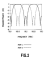
- Fig. 2 shows the transmission characteristics of the interleaver. These transmission characteristics are observed at a first and second output waveguides when an optical signal is input to a first input waveguide. Both transparencies form the first input waveguide to the first and second output waveguides have stop bands where the optical signal is prohibited and pass bands where the optical signals is allowed to go through in an alternative manner. Further, when light at a frequency is allowed to go to the first waveguide (the pass band), the light is not allowed to go to the second waveguide (the stop band), and vice versa.
- As shown in Fig. 3, an optical multi/demultiplexer of 50 GHz channel spacing can be implemented by combining the
interleaver 110 with optical multi/demultiplexers interleaver 110. To avoid degrading the transmission characteristics of an optical multi/demultiplexer of a narrow channel spacing, the transmission characteristics of the interleaver must be such that for a pass band, transmittance is close to 1 over a relatively wide range of optical frequencies, and for a stop band, transmittance is close to 0 over a relatively wide range of optical frequencies. - However, the conventional interleaver has the following problems: first, the conventional interleaver has only two outputs but has more than two parameters to be set. Accordingly, adjustment of the parameters is very complicated. In the example shown in Fig. 1, coupler splitting ratio must be set for three locations, and phase must be set for two locations. Thus, a total of five parameters must be set.
- Second, the conventional interleaver has delay lines arranged in series, so that if half wave plates are used to compensate for birefringence in the optical waveguides, a half wave plate must be inserted into each stage. As a result, excess losses increase. Further, to compensate for the dependence of the optical waveguides on temperature, material (hereinafter referred to as "temperature compensating material") whose refractive index change with a temperature has an opposite sign to that of the optical waveguides must be inserted into each stage. As a result, excess losses increase.
- Third, instead of realizing the flat characteristics of pass bands using a smaller number of stages, the conventional interleaver has non-linear phase characteristics. As a result, the pass bands have chromatic dispersion. Such chromatic dispersion may cause signal quality to be degraded when interleavers are used in a long-distance high-speed optical transmission system.
- It is an object of the present invention to provide an optical filter which allows parameters to be easily adjusted, which allows birefringence and temperature dependence to be easily compensated for, and which is essentially free from dispersion.
- To attain this objects, an optical filter comprises an input optical waveguide, a first optical coupler that splits an optical signal guided by the input optical waveguide into two parts, at least one optical splitting means connected to an output of the first optical coupler, two groups of optical waveguide delay lines (the minimum number of constituents of the group is 1) connected to outputs of the optical splitting means, or an output of the optical coupler and an output of the optical splitting means, at least one optical combining means for combining any lights from the two groups of optical waveguide delay lines, a second optical coupler having a symmetric power splitting ratio and connected to outputs of the optical combining means, or an output of the optical combining means and the optical waveguide delay line, and an output optical waveguide connected to an output of the second optical coupler, all of said components being formed on a substrate, and wherein delay time provided by one of the two groups of optical waveguide delay lines is set to be τ0+2nΔτ+αn (τ0 and Δτ are positive real numbers, n is an integer that varies with optical waveguide delay line, |αn| ≤λ/u, λ is a wavelength, and u is the speed of light propagating through the waveguides), and delay time provided by the other group of optical waveguide delay lines is set to be τ0+(2m+1)Δτ+βm (m is an integer that varies with optical waveguide delay line, |βm|≤λ/u).
- The above and other objects, effects, features and advantages of the present invention will become more apparent from the following description of embodiments thereof taken in conjunction with the accompanying drawings.
- Fig. 1 is a diagram showing the configuration of a conventional interleaver;
- Fig. 2 is a chart showing the transmission characteristics of the conventional interleaver;
- Fig. 3 is a diagram showing an example of the usage of the conventional interleaver;
- Fig. 4 is a diagram showing an optical filter according to a first embodiment of the present invention;
- Fig. 5 is a chart showing the transmission characteristics of the optical filter of the first embodiment;
- Fig. 6 is a diagram showing the configuration of an optical filter according to a second embodiment of the present invention;
- Fig. 7 is a diagram showing the configuration of an optical coupler with a tunable coupling ratio;
- Fig. 8 is a diagram showing the configuration of an optical filter according to a third embodiment of the present invention;
- Fig. 9 is a chart showing the transmission characteristics of the optical filter of the third embodiment;
- Fig. 10 is a diagram showing the configuration of an optical filter according to a fourth embodiment of the present invention;
- Fig. 11 is a diagram showing the configuration of an optical filter according to a fifth embodiment of the present invention;
- Fig. 12 is a chart showing the transmission characteristics of the optical filter of the fifth embodiment;
- Fig. 13 is a diagram showing the configuration of an optical filter according to a sixth embodiment of the present invention;
- Fig. 14 is a diagram showing the configuration of an optical filter according to a seventh embodiment of the present invention; and
- Fig. 15 is a diagram showing the configuration of an optical filter according to an eighth embodiment of the present invention.
-
- Embodiments of the present invention will be described below with reference to the drawings. In this embodiment, a silica-based optical waveguide will be described which has optical waveguides formed on a silicon substrate. The silica-based optical waveguide can be connected to optical fibers with low losses, thereby providing a stable and inexpensive optical filter. However, the present invention is not limited to this embodiment, but other optical waveguides may be used such as a semiconductor optical waveguide, a polymer optical waveguide, and a dielectric optical waveguide. Further, in the following description, for simplification, those optical element circuits which have the same functions are denoted by the same symbols, and duplicate description is avoided.
- Fig. 4 shows an optical filter according to a first embodiment of the present invention. The optical filter has a
substrate 10, inputoptical waveguides optical coupler 12. Theoptical coupler 12 has 1×2optical coupler 13a connected to one output thereof and corresponding to optical splitting means. Theoptical coupler 12 has 1×2optical coupler 13b connected to the other output thereof and corresponding to optical splitting means. - The optical filter has two groups of optical waveguide delay lines consisting of a first group of optical
waveguide delay lines optical coupler 13a and a second group of opticalwaveguide delay lines optical coupler 13b. In a first embodiment, each of the two groups of optical waveguide delay lines is composed of two optical waveguides. The two optical waveguides are provided because an effective interleaver can be easily constructed. However, the present invention is not limited to this example, but a combination of another number of optical waveguides may be used. - The first group of optical
waveguide delay lines optical coupler 16a connected to an output thereof and corresponding to optical combining means. The second group of opticalwaveguide delay lines optical coupler 16b connected to an output thereof and corresponding to optical combining means. Furthermore, the optical filter has amultimode interference coupler 17 having a splitting ratio of 0.5 and which combines light from the 2×1optical coupler 16a with light from the 2×1optical coupler 16b, themultimode interference coupler 17 corresponding to a second optical coupler, and outputoptical waveguides - In this case, absolute delay time provided by the optical
waveguide delay line 14a is defined as τ0. Relative delay time provided by the opticalwaveguide delay line 14a is defined as 0Δτ+0.5λ/u. Reference character λ denotes a center wavelength of light for use in the optical filter. Reference character u denotes the speed of light propagating through the optical waveguides. In this case, a delay time difference provided by the opticalwaveguide delay line 14b is 2Δτ. Delay time provided by the opticalwaveguide delay line 15a is Δτ. Delay time provided by the opticalwaveguide delay line 15b is 3Δτ. - In this case, the absolute delay time provided by the optical
waveguide delay line 14 is generalized as τ0 + 2nΔτ+αn. For αn, |αn|≤λ/u. Reference character λ denotes a center wavelength of light for use in the optical filter. Reference character u denotes the speed of light propagating through the optical waveguides. Similarly, absolute delay time provided by the opticalwaveguide delay line 15 is τ0+(2m+1) Δτ+βm. For βm, |βm|≤λ/u. - The
optical coupler 12 has a splitting ratio of 0.7. Theoptical couplers optical couplers optical couplers optical couplers optical couplers optical couplers - In the optical filter of the first embodiment, the
optical coupler 17 is composed of a multimode interference coupler because it is excellent in reproducibility. However, the present invention is not limited to this example. Of course, another coupler such as a directional coupler may be used. - Further, the optical filter of the first embodiment is characterized in that circuit parameters can be easily extracted and set because the optical waveguide delay lines provide different amounts of delay and because the circuit parameters can thus be easily estimated using a method such as Fourier transform spectroscopy.
- Fig. 5 shows the transmission characteristics of the optical filter according to the first embodiment shown in Fig. 4. This figure shows the optical frequency transmission characteristics for transmission of light from the input
optical waveguide 11a to theoutput waveguides output waveguide 18a and light output to theoutput waveguide 18b alternately have pass bands where optical signals pass and stop bands where no optical signals pass. The optical frequency transmission characteristics of light output to theoutput waveguide 18a and of light output to theoutput waveguide 18b are such that when one of the characteristics has a pass band, the other has a stop band. - Fig. 6 shows a second embodiment as a variation of the first embodiment, shown in Fig. 4. The second embodiment includes not only the configuration of the optical filter according to the first embodiment but also an optical coupler with a tunable coupling ratio as the first
optical coupler 12. Further,thin film heaters waveguide delay lines Thin film heaters waveguide delay lines - Since the optical coupler with the tunable coupling ratio is used as the
optical coupler 12, any characteristic of the optical filter which has deviated from the corresponding set value owing to a manufacture error or the like, particularly a reduced extinction ratio for stop bands can be compensated for. - The optical coupler with the tunable coupling ratio may be composed of the Mach-Zehnder interferometer shown in Fig. 7. The Mach-Zehnder interferometer is composed of an
optical coupler 29,optical waveguides optical coupler 31. The Mach-Zehnder interferometer is only an example of implementation of the optical coupler with the tunable coupling ratio. The optical coupler with the tunable coupling ratio may be implemented using another means such as light irradiation or annealing. - Further, the phase adjusters shown in Fig. 7 make adjustments on the basis of thermooptic effects using the heaters. However, the present invention is not limited to this example. For example, the phase adjusters may be implemented using another means such as electro-optic effects.
- According to the second embodiment, the optical filter is provided with the
thin film heaters waveguide delay lines thin film heaters waveguide delay lines waveguide delay lines - In the second embodiment, shown in Fig. 6, the thin film heaters are used as stable and reliable phase adjusting means. However, the present invention is not limited to this example. Phase adjustment may be carried out using another means such as application of light or heat.
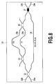
- Fig. 8 shows an optical filter according to a third embodiment of the present invention. This optical filter has the
substrate 10, the inputoptical waveguides optical coupler 12 that splits light from the inputoptical waveguides optical coupler 12 has a 1×2optical coupler 13 connected to one output thereof and corresponding to optical splitting means. - The optical filter has two groups of optical waveguide delay lines consisting of a
first group 14 of optical waveguide delay lines connected to the other output of theoptical coupler 12 and a second group of opticalwaveguide delay lines optical coupler 13. In the third embodiment, the first group includes one optical waveguide, and the second group includes two optical waveguides. Thus, the optical waveguide delay line may be composed of only one optical waveguide. However, the present invention is not limited to this example. A combination of other numbers of optical waveguides may be used. - The second group of optical
waveguide delay lines optical coupler 16 connected to an output thereof and corresponding to optical combining means. Furthermore, the optical filter has the secondoptical coupler 17 having a splitting ratio of 0.5 and which combines light from the 2×1optical coupler 16 with light from thefirst group 14 of optical waveguide delay lines, and the outputoptical waveguides optical coupler 17. - In this case, if relative delay time provided by the optical
waveguide delay line 14 is defined as 0Δτ+0.5λ/u, then a delay time difference provided by the opticalwaveguide delay line 15a is Δτ. Further, delay time provided by the opticalwaveguide delay line 15b is 3Δτ. Reference character λ denotes a center wavelength of light for use in the optical filter. - The
optical coupler 12 has a splitting ratio of 0.58. Theoptical couplers optical couplers optical couplers - In the optical filter of the third embodiment, the
optical coupler 17 is composed of a multimode interference coupler because it is excellent in reproducibility. However, the present invention is not limited to this example. Of course, another coupler such as a directional coupler may be used. - Further, the optical filter of the third embodiment is characterized in that circuit parameters can be easily extracted and set because the optical waveguide delay lines provide different amounts of delay and because the circuit parameters can thus be easily estimated using a method such as Fourier transform spectroscopy.
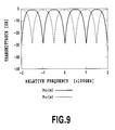
- Fig. 9 shows the transmission characteristics of the optical filter according to the third embodiment shown in Fig. 8. This figure shows the optical frequency transmission characteristics for transmission of light from the input
optical waveguide 11a to theoutput waveguides output waveguide 18a and light output to theoutput waveguide 18b alternately have pass bands where optical signals pass and stop bands where no optical signals pass. The optical frequency transmission characteristics of light output to theoutput waveguide 18a and of light output to theoutput waveguide 18b are such that when one of the characteristics has a pass band, the other has a stop band. - In the optical filter of the third embodiment, an optical coupler with a tunable coupling ratio can be used as the
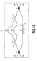
optical coupler 12 as in the case of Fig. 6 to compensate for the deviation of the splitting ratio of the optical couplers due to a manufacture error or the like. Further, in the optical filter of the third embodiment, if the opticalwaveguide delay lines wavelength delay lines - Fig. 10 shows a fourth embodiment as a variation of the third embodiment shown in Fig. 8. The fourth embodiment includes the configuration of the optical filter according to the third embodiment. However, the first optical coupler has a splitting ratio of 0.5, and the optical
waveguide delay line 14 is provided with anoptical amplitude adjuster 21. Thus, the quantity of light guided to the opticalwaveguide delay line 15 is adjusted to reproducibly obtain the desired characteristics of the optical filter. - The
optical amplitude adjuster 21 may be composed of the Mach-Zehnder interferometer shown in Fig. 7. The Mach-Zehnder interferometer is composed of theoptical coupler 29, theoptical waveguides optical coupler 31. The Mach-Zehnder interferometer is only an example of implementation of the optical amplitude adjuster. The optical amplitude adjuster may be implemented using another means. - The phase adjusters shown in Fig. 7 make adjustments on the basis of thermooptic effects using the heaters. However, the present invention is not limited to this example. For example, the phase adjusters may be implemented using another means such as electro-optic effects.
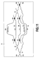
- Fig. 11 shows an optical filter according to a fifth embodiment of the present invention. This optical filter has the
substrate 10, the inputoptical waveguides optical coupler 12 that splits light from the inputoptical waveguides optical coupler 12 has a 1×2optical coupler 22 connected to one output thereof and corresponding to optical splitting means. - The optical filter has two groups of optical waveguide delay lines consisting of the
first group 14 of optical waveguide delay lines connected to the other output of theoptical coupler 12,multimode interference couplers output coupler 22 and having a splitting ratio of 0.5, and a second group of opticalwaveguide delay lines 15a to 15d connected to outputs of themultimode interference couplers - The second group of optical
waveguide delay lines 15a to 15d havemultimode interference couplers optical coupler 25 couples outputs from themultimode interference couplers optical coupler 17 having a splitting ratio of 0.5 and which combines light from the 2×1optical coupler 25 with light from thefirst group 14 of optical waveguide delay lines, and the outputoptical waveguides optical coupler 17. - In this case, if relative delay time provided by the optical
waveguide delay line 14 is defined as 0Δτ, then delay time difference provided by the opticalwaveguide delay line 15a is Δτ+0.5λ/u. Further, delay time provided by the opticalwaveguide delay line 15b is -Δτ. Delay time provided by the opticalwaveguide delay line 15c is -3Δτ. Delay time provided by the opticalwaveguide delay line 15d is 3Δτ+0.5λ/u. Reference character λ denotes a center wavelength of light for use in the optical filter. - The
optical coupler 12 has a splitting ratio of 0.39. Theoptical couplers optical couplers optical couplers - In the optical filter of the fifth embodiment, the
optical couplers - Further, the optical filter of the fifth embodiment is constructed so that equal light intensity is guided to the
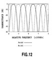
optical waveguides optical waveguides - Fig. 12 shows the transmission characteristics of the optical filter according to the fifth embodiment shown in Fig. 11. This figure shows the optical frequency transmission characteristics for transmission of light from the input
optical waveguide 11a to theoutput waveguides output waveguide 18a and light output to theoutput waveguide 18b alternately have pass bands where optical signals pass and stop bands where no optical signals pass. The optical frequency transmission characteristics of light output to theoutput waveguide 18a and of light output to theoutput waveguide 18b are such that when one of the characteristics has a pass band, the other has a stop band. - Fig. 13 shows a sixth embodiment as a first variation of the fifth embodiment, shown in Fig. 11. The second embodiment includes not only the configuration of the optical filter according to the fifth embodiment but also an optical coupler with a tunable coupling ratio as the first
optical coupler 12. With this configuration, in spite of a manufacture error or the like, theoptical coupler 12 can be adjusted to obtain the desired characteristics of the optical filter. - In the sixth embodiment,
thin film heaters 20a to 20d are provided on the opticalwaveguide delay lines waveguide delay lines - Further, the optical
waveguide delay line 14 is provided with theoptical amplitude adjuster 21. Theoptical amplitude adjuster 21 may be composed of the Mach-Zehnder interferometer shown in Fig. 7. The Mach-Zehnder interferometer is composed of theoptical coupler 29, theoptical waveguides optical coupler 31. The Mach-Zehnder interferometer is only an example of implementation of the optical amplitude adjuster. The optical amplitude adjuster may be implemented using another means. - The phase adjusters shown in Fig. 7 make adjustments on the basis of thermooptic effects using the heaters. However, the present invention is not limited to this example. For example, the phase adjusters may be implemented using another means such as electro-optic effects.
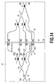
- Fig. 14 shows a seventh embodiment as a second variation of the fifth embodiment, shown in Fig. 12. The seventh embodiment includes the configuration of the optical filter according to the sixth embodiment, shown in Fig. 13. However, the optical filter is generally laterally symmetric with a
groove 26 formed at a symmetry axis and crossing the optical waveguides. Thegroove 26 has ahalf wave plate 27 inserted thereinto and having a birefringence axis tilted through 45° from the birefringence axes of the optical waveguides. - With this configuration, the effects of birefringence of the optical waveguides are offset to eliminate the dependence of the optical filter on polarization such as a variation in transmittance depending on polarization. The half wave plate may be composed of polyimide, silica, or other material.
- Fig. 15 shows an eighth embodiment as a third variation of the fifth embodiment, shown in Fig. 11. The eighth embodiment includes the configuration of the optical filter according to the seventh embodiment, shown in Fig. 14. However, the optical
waveguide delay lines materials 28a to 28d the dependence of the refractive index of which has a sign different from that of the optical waveguides. - With this configuration, even if the refractive index of the optical waveguides varies with temperature, the effects of the variation are canceled. Therefore, an optical filter is obtained which is generally independent of temperature.
- The present invention has been described in detail with respect to preferred embodiments, and it will now be apparent from the foregoing to those skilled in the art that changes and modifications may be made without departing from the invention in its broader aspect, and it is the intention, therefore, in the apparent claims to cover all such changes and modifications as fall within the true spirit of the invention.
Claims (11)
- An optical filter characterized by comprising:wherein delay time provided by one of said two groups of optical waveguide delay lines is set to be τ0+2nΔτ+αn (τ0 and Δτ are positive real numbers, n is an integer that varies with optical waveguide delay line, |αn| ≤λ/u, λ is a wavelength, and u is the speed of light propagating through the waveguides), andan input optical waveguide;a first optical coupler that splits an optical signal guided by said input optical waveguide into two parts;at least one optical splitting means connected to an output of said first optical coupler;two groups of optical waveguide delay lines (the minimum number of constituents of the group is 1) connected to outputs of said optical splitting means, or an output of said first optical coupler and an output of said optical splitting means;at least one optical combining means for combining any lights from said two groups of optical waveguide delay lines;a second optical coupler having a symmetric power splitting ratio and connected to outputs of said optical combining means, or an output of said optical combining means and the optical waveguide delay line; andan output optical waveguide connected to an output of said second optical coupler, all of said components being formed on a substrate, and
delay time provided by the other group of optical waveguide delay lines is set to be τ0+(2m+1)Δτ+βm (m is an integer that varies with optical waveguide delay line, |βm|≤λ/u). - An optical filter according to claim 1, characterized in that the splitting rations of said optical splitting means and said optical combining means are set to be substantially equal.
- An optical filter according to claim 1, characterized in that said first optical coupler has a tunable coupling ratio.
- An optical filter according to claim 1, characterized in that at least one optical amplitude adjusting means is provided between said first optical coupler and said second optical coupler.
- An optical filter according to claim 1, characterized in that said two groups of optical waveguide delay lines are set so that equal light intensity is guided to optical waveguides providing delay time τ0±kΔτ (k is a real number).
- An optical filter according to claim 1, characterized in that said optical waveguide delay line comprises phase adjusting means.
- An optical filter according to claim 1, characterized in that said optical waveguide delay line has a half wave plate inserted at a substantially intermediate point thereof.
- An optical filter according to claim 1, characterized in that said optical waveguide delay line has one or more grooves formed therein and into which material is inserted, the material having a refractive index thermal coefficient having a sign different from the thermal coefficient of the effective refractive index of the optical waveguides.
- An optical filter according to claim 1, characterized in that said optical coupler having the symmetric power splitting ratio is a multimode interference coupler.
- An optical filter according to claim 4, characterized in that said optical waveguide is based on silica, and said optical amplitude adjusting means is a Mach-Zehnder interferometer provided with thermooptic phase shifters.
- An optical filter according to claim 6, characterized in that said optical waveguide is based on silica, and said optical amplitude adjusting means is a thermooptic phase shifter.
Applications Claiming Priority (2)
| Application Number | Priority Date | Filing Date | Title |
|---|---|---|---|
| JP2001241367 | 2001-08-08 | ||
| JP2001241367A JP2003057457A (en) | 2001-08-08 | 2001-08-08 | Optical filter |
Publications (3)
| Publication Number | Publication Date |
|---|---|
| EP1286192A2 true EP1286192A2 (en) | 2003-02-26 |
| EP1286192A3 EP1286192A3 (en) | 2003-11-12 |
| EP1286192B1 EP1286192B1 (en) | 2006-03-22 |
Family
ID=19071823
Family Applications (1)
| Application Number | Title | Priority Date | Filing Date |
|---|---|---|---|
| EP02255532A Expired - Fee Related EP1286192B1 (en) | 2001-08-08 | 2002-08-07 | Optical waveguide filter |
Country Status (4)
| Country | Link |
|---|---|
| US (1) | US6724957B2 (en) |
| EP (1) | EP1286192B1 (en) |
| JP (1) | JP2003057457A (en) |
| DE (1) | DE60210018T2 (en) |
Cited By (2)
| Publication number | Priority date | Publication date | Assignee | Title |
|---|---|---|---|---|
| WO2004038493A1 (en) * | 2002-10-25 | 2004-05-06 | The Furukawa Electric Co., Ltd. | Dynamic gain equalizer |
| WO2009003864A1 (en) * | 2007-07-04 | 2009-01-08 | Fraunhofer Gesellschaft zur Förderung der angewandten Forschung e.V. | Method and apparatus for compensating polarization-dependent frequency shifts in optical waveguides |
Families Citing this family (18)
| Publication number | Priority date | Publication date | Assignee | Title |
|---|---|---|---|---|
| JP2002341165A (en) * | 2001-05-15 | 2002-11-27 | Furukawa Electric Co Ltd:The | Optical wavelength multiplexing and demultiplexing device, and method for using the same |
| JP3802838B2 (en) * | 2001-05-30 | 2006-07-26 | 古河電気工業株式会社 | Optical multiplexer / demultiplexer |
| US7171067B2 (en) * | 2003-03-03 | 2007-01-30 | Lucent Technologies Inc. | Integrateable optical interleaver and de-interleaver |
| US6768843B1 (en) * | 2002-08-16 | 2004-07-27 | Wavesplitter Technologies, Inc. | Cascaded fourier filter interleaver having enhanced performance |
| JP4593080B2 (en) * | 2003-03-28 | 2010-12-08 | 古河電気工業株式会社 | Optical monitoring device |
| US7254293B1 (en) * | 2003-06-30 | 2007-08-07 | Calient Networks, Inc. | Wavelength routing optical switch |
| US8639069B1 (en) | 2003-06-30 | 2014-01-28 | Calient Technologies, Inc. | Wavelength dependent optical switch |
| JP4550630B2 (en) * | 2005-03-11 | 2010-09-22 | 古河電気工業株式会社 | Variable dispersion compensator |
| EP2597457B1 (en) | 2005-07-28 | 2018-03-14 | Bioptigen, Inc. | Frequency-domain optical coherence tomography imaging system |
| JP5399693B2 (en) * | 2008-07-14 | 2014-01-29 | 日本電信電話株式会社 | Optical wavelength multiplexing / demultiplexing circuit |
| US8224139B2 (en) * | 2008-08-21 | 2012-07-17 | Infinera Corporation | Tunable optical filter |
| US8644653B2 (en) * | 2010-09-01 | 2014-02-04 | Infinera Corporation | Compact multimode interference element |
| JP2012215692A (en) * | 2011-03-31 | 2012-11-08 | Furukawa Electric Co Ltd:The | Polarization separation element and optical integrated device |
| US20140293393A1 (en) * | 2013-03-28 | 2014-10-02 | Barthelemy Fondeur | Flat-top tunable filter |
| CN104125517B (en) * | 2013-04-26 | 2019-02-22 | 中兴通讯股份有限公司 | A kind of optical transmission system, mode coupler and optical transmission method |
| JP6266315B2 (en) * | 2013-11-14 | 2018-01-24 | 富士通株式会社 | Wavelength multiplexer / demultiplexer and optical integrated circuit device |
| EP3749991A4 (en) | 2018-02-05 | 2021-10-20 | GC Photonics Inc. | Variable optical filter |
| WO2023147402A2 (en) * | 2022-01-27 | 2023-08-03 | Nubis Communications, Inc. | Optical equalizer with bidirectional reentry for intersymbol interference mitigation |
Citations (2)
| Publication number | Priority date | Publication date | Assignee | Title |
|---|---|---|---|---|
| WO2000070402A1 (en) * | 1999-05-12 | 2000-11-23 | Siemens Aktiengesellschaft | Method and arrangement of a modulator for multistaged shift-keyed polarised optical signals |
| US6212315B1 (en) * | 1998-07-07 | 2001-04-03 | Lucent Technologies Inc. | Channel power equalizer for a wavelength division multiplexed system |
Family Cites Families (4)
| Publication number | Priority date | Publication date | Assignee | Title |
|---|---|---|---|---|
| US5351317A (en) * | 1992-08-14 | 1994-09-27 | Telefonaktiebolaget L M Ericsson | Interferometric tunable optical filter |
| US5930414A (en) * | 1997-09-16 | 1999-07-27 | Lucent Technologies Inc. | Method and apparatus for automatic compensation of first-order polarization mode dispersion (PMD) |
| US6351581B1 (en) * | 1998-03-17 | 2002-02-26 | Agere Systems Optoelectronics Guardian Corp. | Optical add-drop multiplexer having an interferometer structure |
| EP1176439A1 (en) * | 2000-07-11 | 2002-01-30 | Corning Incorporated | Tapped delay line based gain flattening filter |
-
2001
- 2001-08-08 JP JP2001241367A patent/JP2003057457A/en active Pending
-
2002
- 2002-08-07 DE DE60210018T patent/DE60210018T2/en not_active Expired - Lifetime
- 2002-08-07 US US10/213,075 patent/US6724957B2/en not_active Expired - Fee Related
- 2002-08-07 EP EP02255532A patent/EP1286192B1/en not_active Expired - Fee Related
Patent Citations (2)
| Publication number | Priority date | Publication date | Assignee | Title |
|---|---|---|---|---|
| US6212315B1 (en) * | 1998-07-07 | 2001-04-03 | Lucent Technologies Inc. | Channel power equalizer for a wavelength division multiplexed system |
| WO2000070402A1 (en) * | 1999-05-12 | 2000-11-23 | Siemens Aktiengesellschaft | Method and arrangement of a modulator for multistaged shift-keyed polarised optical signals |
Non-Patent Citations (3)
| Title |
|---|
| JINGUJI K ET AL: "TWO-PORT OPTICAL WAVELENGTH CIRCUITS COMPOSED OF CASCADED MACH- ZEHNDER INTERFEROMETERS WITH POINT-SYMMETRICAL CONFIGURATIONS" JOURNAL OF LIGHTWAVE TECHNOLOGY, IEEE. NEW YORK, US, vol. 14, no. 10, 1 October 1996 (1996-10-01), pages 2301-2310, XP000631532 ISSN: 0733-8724 * |
| OGUMA M ET AL: "Flat-top and low-loss WDM filter composed of lattice-form interleave filter and arrayed-waveguide gratings on one chip" OPTICAL FIBER COMMUNICATION CONFERENCE. (OFC). TECHNICAL DIGEST POSTCONFERENCE EDITION. ANAHEIM, CA, MARCH 17 - 22, 2001, TRENDS IN OPTICS AND PHOTONICS SERIES. TOPS. VOLUME 54, WASHINGTON, WA: OSA, US, vol. 1 OF 4, 2001, pages wb3-1-wb3-3, XP010546334 ISBN: 1-55752-655-9 * |
| SASAYAMA K ET AL: "COHERENT OPTICAL TRANSVERSAL FILTER USING SILICA-BASED SINGLE-MODE WAVEGUIDES" ELECTRONICS LETTERS, IEE STEVENAGE, GB, vol. 26, no. 22, 26 October 1989 (1989-10-26), pages 1508-1509, XP000076242 ISSN: 0013-5194 * |
Cited By (4)
| Publication number | Priority date | Publication date | Assignee | Title |
|---|---|---|---|---|
| WO2004038493A1 (en) * | 2002-10-25 | 2004-05-06 | The Furukawa Electric Co., Ltd. | Dynamic gain equalizer |
| US7146079B2 (en) | 2002-10-25 | 2006-12-05 | The Furukawa Electric Co., Ltd. | Dynamic gain equalizer |
| WO2009003864A1 (en) * | 2007-07-04 | 2009-01-08 | Fraunhofer Gesellschaft zur Förderung der angewandten Forschung e.V. | Method and apparatus for compensating polarization-dependent frequency shifts in optical waveguides |
| US8295656B2 (en) | 2007-07-04 | 2012-10-23 | Fraunhofer-Gesellschaft zur Förderung der angewandten Forschung e.V. | Method and apparatus for compensating polarization-dependent frequency shifts in optical waveguides |
Also Published As
| Publication number | Publication date |
|---|---|
| US20030031406A1 (en) | 2003-02-13 |
| DE60210018D1 (en) | 2006-05-11 |
| EP1286192A3 (en) | 2003-11-12 |
| JP2003057457A (en) | 2003-02-26 |
| US6724957B2 (en) | 2004-04-20 |
| EP1286192B1 (en) | 2006-03-22 |
| DE60210018T2 (en) | 2006-08-24 |
Similar Documents
| Publication | Publication Date | Title |
|---|---|---|
| US6724957B2 (en) | Optical filter | |
| US7492983B2 (en) | Optical circuit device | |
| JP4559171B2 (en) | Adjustable dispersion compensator | |
| US7899279B2 (en) | Optical delay line interferometer | |
| US7020398B2 (en) | Dispersion slope equalizer | |
| EP1191364B1 (en) | Waveguide optical interferometer | |
| EP1065821B1 (en) | Optical system | |
| US8433196B2 (en) | Optical band splitter/combiner device comprising a three-arms interferometer | |
| US10274680B2 (en) | Delay line interferometer with polarization compensation at selective frequency | |
| Wang et al. | A high-performance ultracompact optical interleaver based on double-ring assisted Mach–Zehnder interferometer | |
| US6606433B2 (en) | Optical multi/demultiplexer | |
| US7027690B2 (en) | Optical waveguide coupler circuit device | |
| Waqas et al. | Cascaded Mach–Zehnder architectures for photonic integrated delay lines | |
| US5425116A (en) | Tunable optical waveguide grating arrangement | |
| EP1343029B1 (en) | Optical waveguide coupler circuit | |
| US20030128926A1 (en) | Compact wavelength routing device having substantially flat passband | |
| US20230228944A1 (en) | Wavelength division multiplexer and demultiplexer | |
| JP2002082241A (en) | Optical multiplexer/demultiplexer | |
| KR20020079577A (en) | Optical multiplexer/demultiplexer | |
| EP1347585A2 (en) | Optical system for gain equalization | |
| Doerr et al. | Two Mach-Zehnder-type tunable dispersion compensators integrated in series to increase bandwidth and/or range while maintaining single-knob control | |
| Mizuno et al. | Uniform wavelength spacing Mach-Zehnder interferometer using phase-generating couplers | |
| Mizuno et al. | Interleave filter based on coherent optical transversal filter | |
| Kohtoku et al. | High performance interleave filters composed of planar lightwave circuits on Si |
Legal Events
| Date | Code | Title | Description |
|---|---|---|---|
| PUAI | Public reference made under article 153(3) epc to a published international application that has entered the european phase |
Free format text: ORIGINAL CODE: 0009012 |
|
| AK | Designated contracting states |
Kind code of ref document: A2 Designated state(s): AT BE BG CH CY CZ DE DK EE ES FI FR GB GR IE IT LI LU MC NL PT SE SK TR |
|
| AX | Request for extension of the european patent |
Extension state: AL LT LV MK RO SI |
|
| PUAL | Search report despatched |
Free format text: ORIGINAL CODE: 0009013 |
|
| AK | Designated contracting states |
Kind code of ref document: A3 Designated state(s): AT BE BG CH CY CZ DE DK EE ES FI FR GB GR IE IT LI LU MC NL PT SE SK TR |
|
| AX | Request for extension of the european patent |
Extension state: AL LT LV MK RO SI |
|
| RIC1 | Information provided on ipc code assigned before grant |
Ipc: 7G 02B 6/34 A Ipc: 7G 02B 6/12 B Ipc: 7H 04J 14/02 B |
|
| 17P | Request for examination filed |
Effective date: 20040426 |
|
| 17Q | First examination report despatched |
Effective date: 20040621 |
|
| AKX | Designation fees paid |
Designated state(s): DE FR GB IT |
|
| GRAP | Despatch of communication of intention to grant a patent |
Free format text: ORIGINAL CODE: EPIDOSNIGR1 |
|
| GRAS | Grant fee paid |
Free format text: ORIGINAL CODE: EPIDOSNIGR3 |
|
| GRAA | (expected) grant |
Free format text: ORIGINAL CODE: 0009210 |
|
| AK | Designated contracting states |
Kind code of ref document: B1 Designated state(s): DE FR GB IT |
|
| REG | Reference to a national code |
Ref country code: GB Ref legal event code: FG4D |
|
| REF | Corresponds to: |
Ref document number: 60210018 Country of ref document: DE Date of ref document: 20060511 Kind code of ref document: P |
|
| ET | Fr: translation filed | ||
| PLBE | No opposition filed within time limit |
Free format text: ORIGINAL CODE: 0009261 |
|
| STAA | Information on the status of an ep patent application or granted ep patent |
Free format text: STATUS: NO OPPOSITION FILED WITHIN TIME LIMIT |
|
| 26N | No opposition filed |
Effective date: 20061227 |
|
| PGFP | Annual fee paid to national office [announced via postgrant information from national office to epo] |
Ref country code: GB Payment date: 20120817 Year of fee payment: 11 |
|
| PGFP | Annual fee paid to national office [announced via postgrant information from national office to epo] |
Ref country code: IT Payment date: 20120822 Year of fee payment: 11 Ref country code: FR Payment date: 20120824 Year of fee payment: 11 Ref country code: DE Payment date: 20120822 Year of fee payment: 11 |
|
| GBPC | Gb: european patent ceased through non-payment of renewal fee |
Effective date: 20130807 |
|
| PG25 | Lapsed in a contracting state [announced via postgrant information from national office to epo] |
Ref country code: DE Free format text: LAPSE BECAUSE OF NON-PAYMENT OF DUE FEES Effective date: 20140301 |
|
| REG | Reference to a national code |
Ref country code: DE Ref legal event code: R119 Ref document number: 60210018 Country of ref document: DE Effective date: 20140301 |
|
| REG | Reference to a national code |
Ref country code: FR Ref legal event code: ST Effective date: 20140430 |
|
| PG25 | Lapsed in a contracting state [announced via postgrant information from national office to epo] |
Ref country code: IT Free format text: LAPSE BECAUSE OF NON-PAYMENT OF DUE FEES Effective date: 20130807 |
|
| PG25 | Lapsed in a contracting state [announced via postgrant information from national office to epo] |
Ref country code: GB Free format text: LAPSE BECAUSE OF NON-PAYMENT OF DUE FEES Effective date: 20130807 |
|
| PG25 | Lapsed in a contracting state [announced via postgrant information from national office to epo] |
Ref country code: FR Free format text: LAPSE BECAUSE OF NON-PAYMENT OF DUE FEES Effective date: 20130902 |