EP1286192A2 - Optical waveguide filter - Google Patents
Optical waveguide filter Download PDFInfo
- Publication number
- EP1286192A2 EP1286192A2 EP02255532A EP02255532A EP1286192A2 EP 1286192 A2 EP1286192 A2 EP 1286192A2 EP 02255532 A EP02255532 A EP 02255532A EP 02255532 A EP02255532 A EP 02255532A EP 1286192 A2 EP1286192 A2 EP 1286192A2
- Authority
- EP
- European Patent Office
- Prior art keywords
- optical
- coupler
- optical waveguide
- filter according
- output
- Prior art date
- Legal status (The legal status is an assumption and is not a legal conclusion. Google has not performed a legal analysis and makes no representation as to the accuracy of the status listed.)
- Granted
Links
Images






Classifications
-
- G—PHYSICS
- G02—OPTICS
- G02B—OPTICAL ELEMENTS, SYSTEMS OR APPARATUS
- G02B6/00—Light guides; Structural details of arrangements comprising light guides and other optical elements, e.g. couplings
- G02B6/24—Coupling light guides
- G02B6/26—Optical coupling means
- G02B6/28—Optical coupling means having data bus means, i.e. plural waveguides interconnected and providing an inherently bidirectional system by mixing and splitting signals
- G02B6/293—Optical coupling means having data bus means, i.e. plural waveguides interconnected and providing an inherently bidirectional system by mixing and splitting signals with wavelength selective means
- G02B6/29346—Optical coupling means having data bus means, i.e. plural waveguides interconnected and providing an inherently bidirectional system by mixing and splitting signals with wavelength selective means operating by wave or beam interference
- G02B6/2935—Mach-Zehnder configuration, i.e. comprising separate splitting and combining means
- G02B6/29352—Mach-Zehnder configuration, i.e. comprising separate splitting and combining means in a light guide
- G02B6/29355—Cascade arrangement of interferometers
-
- G—PHYSICS
- G02—OPTICS
- G02B—OPTICAL ELEMENTS, SYSTEMS OR APPARATUS
- G02B6/00—Light guides; Structural details of arrangements comprising light guides and other optical elements, e.g. couplings
- G02B6/24—Coupling light guides
- G02B6/26—Optical coupling means
- G02B6/28—Optical coupling means having data bus means, i.e. plural waveguides interconnected and providing an inherently bidirectional system by mixing and splitting signals
- G02B6/293—Optical coupling means having data bus means, i.e. plural waveguides interconnected and providing an inherently bidirectional system by mixing and splitting signals with wavelength selective means
- G02B6/29379—Optical coupling means having data bus means, i.e. plural waveguides interconnected and providing an inherently bidirectional system by mixing and splitting signals with wavelength selective means characterised by the function or use of the complete device
- G02B6/2938—Optical coupling means having data bus means, i.e. plural waveguides interconnected and providing an inherently bidirectional system by mixing and splitting signals with wavelength selective means characterised by the function or use of the complete device for multiplexing or demultiplexing, i.e. combining or separating wavelengths, e.g. 1xN, NxM
- G02B6/29386—Interleaving or deinterleaving, i.e. separating or mixing subsets of optical signals, e.g. combining even and odd channels into a single optical signal
-
- G—PHYSICS
- G02—OPTICS
- G02B—OPTICAL ELEMENTS, SYSTEMS OR APPARATUS
- G02B6/00—Light guides; Structural details of arrangements comprising light guides and other optical elements, e.g. couplings
- G02B6/10—Light guides; Structural details of arrangements comprising light guides and other optical elements, e.g. couplings of the optical waveguide type
- G02B6/12—Light guides; Structural details of arrangements comprising light guides and other optical elements, e.g. couplings of the optical waveguide type of the integrated circuit kind
- G02B2006/12133—Functions
- G02B2006/12135—Temperature control
-
- G—PHYSICS
- G02—OPTICS
- G02B—OPTICAL ELEMENTS, SYSTEMS OR APPARATUS
- G02B6/00—Light guides; Structural details of arrangements comprising light guides and other optical elements, e.g. couplings
- G02B6/10—Light guides; Structural details of arrangements comprising light guides and other optical elements, e.g. couplings of the optical waveguide type
- G02B6/12—Light guides; Structural details of arrangements comprising light guides and other optical elements, e.g. couplings of the optical waveguide type of the integrated circuit kind
- G02B2006/12133—Functions
- G02B2006/12159—Interferometer
-
- G—PHYSICS
- G02—OPTICS
- G02B—OPTICAL ELEMENTS, SYSTEMS OR APPARATUS
- G02B6/00—Light guides; Structural details of arrangements comprising light guides and other optical elements, e.g. couplings
- G02B6/10—Light guides; Structural details of arrangements comprising light guides and other optical elements, e.g. couplings of the optical waveguide type
- G02B6/105—Light guides; Structural details of arrangements comprising light guides and other optical elements, e.g. couplings of the optical waveguide type having optical polarisation effects
-
- G—PHYSICS
- G02—OPTICS
- G02B—OPTICAL ELEMENTS, SYSTEMS OR APPARATUS
- G02B6/00—Light guides; Structural details of arrangements comprising light guides and other optical elements, e.g. couplings
- G02B6/24—Coupling light guides
- G02B6/26—Optical coupling means
- G02B6/28—Optical coupling means having data bus means, i.e. plural waveguides interconnected and providing an inherently bidirectional system by mixing and splitting signals
- G02B6/293—Optical coupling means having data bus means, i.e. plural waveguides interconnected and providing an inherently bidirectional system by mixing and splitting signals with wavelength selective means
- G02B6/29379—Optical coupling means having data bus means, i.e. plural waveguides interconnected and providing an inherently bidirectional system by mixing and splitting signals with wavelength selective means characterised by the function or use of the complete device
- G02B6/2938—Optical coupling means having data bus means, i.e. plural waveguides interconnected and providing an inherently bidirectional system by mixing and splitting signals with wavelength selective means characterised by the function or use of the complete device for multiplexing or demultiplexing, i.e. combining or separating wavelengths, e.g. 1xN, NxM
Definitions
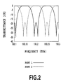
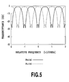
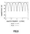
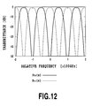
- the conventional interleaver instead of realizing the flat characteristics of pass bands using a smaller number of stages, the conventional interleaver has non-linear phase characteristics. As a result, the pass bands have chromatic dispersion. Such chromatic dispersion may cause signal quality to be degraded when interleavers are used in a long-distance high-speed optical transmission system.
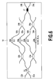
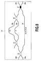
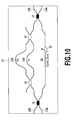
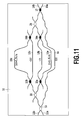
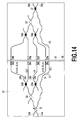
- the optical filter has two groups of optical waveguide delay lines consisting of a first group of optical waveguide delay lines 14a and 14b connected to an output of the 1 ⁇ 2 optical coupler 13a and a second group of optical waveguide delay lines 15a and 15b connected to an output of the 1 ⁇ 2 optical coupler 13b.
- each of the two groups of optical waveguide delay lines is composed of two optical waveguides.
- the two optical waveguides are provided because an effective interleaver can be easily constructed.
- the present invention is not limited to this example, but a combination of another number of optical waveguides may be used.
- the second group of optical waveguide delay lines 15a to 15d have multimode interference couplers 24a and 24b connected to outputs thereof and corresponding to optical combining means.
- a 2 ⁇ 1 optical coupler 25 couples outputs from the multimode interference couplers 24a and 24b together.
- the optical filter has the second optical coupler 17 having a splitting ratio of 0.5 and which combines light from the 2 ⁇ 1 optical coupler 25 with light from the first group 14 of optical waveguide delay lines, and the output optical waveguides 18a and 18b that guide outputs from the optical coupler 17.
Landscapes
- Physics & Mathematics (AREA)
- General Physics & Mathematics (AREA)
- Optics & Photonics (AREA)
- Optical Integrated Circuits (AREA)
- Optical Modulation, Optical Deflection, Nonlinear Optics, Optical Demodulation, Optical Logic Elements (AREA)
Abstract
Description
Claims (11)
- An optical filter characterized by comprising:wherein delay time provided by one of said two groups of optical waveguide delay lines is set to be τ0+2nΔτ+αn (τ0 and Δτ are positive real numbers, n is an integer that varies with optical waveguide delay line, |αn| ≤λ/u, λ is a wavelength, and u is the speed of light propagating through the waveguides), andan input optical waveguide;a first optical coupler that splits an optical signal guided by said input optical waveguide into two parts;at least one optical splitting means connected to an output of said first optical coupler;two groups of optical waveguide delay lines (the minimum number of constituents of the group is 1) connected to outputs of said optical splitting means, or an output of said first optical coupler and an output of said optical splitting means;at least one optical combining means for combining any lights from said two groups of optical waveguide delay lines;a second optical coupler having a symmetric power splitting ratio and connected to outputs of said optical combining means, or an output of said optical combining means and the optical waveguide delay line; andan output optical waveguide connected to an output of said second optical coupler, all of said components being formed on a substrate, and
delay time provided by the other group of optical waveguide delay lines is set to be τ0+(2m+1)Δτ+βm (m is an integer that varies with optical waveguide delay line, |βm|≤λ/u). - An optical filter according to claim 1, characterized in that the splitting rations of said optical splitting means and said optical combining means are set to be substantially equal.
- An optical filter according to claim 1, characterized in that said first optical coupler has a tunable coupling ratio.
- An optical filter according to claim 1, characterized in that at least one optical amplitude adjusting means is provided between said first optical coupler and said second optical coupler.
- An optical filter according to claim 1, characterized in that said two groups of optical waveguide delay lines are set so that equal light intensity is guided to optical waveguides providing delay time τ0±kΔτ (k is a real number).
- An optical filter according to claim 1, characterized in that said optical waveguide delay line comprises phase adjusting means.
- An optical filter according to claim 1, characterized in that said optical waveguide delay line has a half wave plate inserted at a substantially intermediate point thereof.
- An optical filter according to claim 1, characterized in that said optical waveguide delay line has one or more grooves formed therein and into which material is inserted, the material having a refractive index thermal coefficient having a sign different from the thermal coefficient of the effective refractive index of the optical waveguides.
- An optical filter according to claim 1, characterized in that said optical coupler having the symmetric power splitting ratio is a multimode interference coupler.
- An optical filter according to claim 4, characterized in that said optical waveguide is based on silica, and said optical amplitude adjusting means is a Mach-Zehnder interferometer provided with thermooptic phase shifters.
- An optical filter according to claim 6, characterized in that said optical waveguide is based on silica, and said optical amplitude adjusting means is a thermooptic phase shifter.
Applications Claiming Priority (2)
| Application Number | Priority Date | Filing Date | Title |
|---|---|---|---|
| JP2001241367 | 2001-08-08 | ||
| JP2001241367A JP2003057457A (en) | 2001-08-08 | 2001-08-08 | Optical filter |
Publications (3)
| Publication Number | Publication Date |
|---|---|
| EP1286192A2 true EP1286192A2 (en) | 2003-02-26 |
| EP1286192A3 EP1286192A3 (en) | 2003-11-12 |
| EP1286192B1 EP1286192B1 (en) | 2006-03-22 |
Family
ID=19071823
Family Applications (1)
| Application Number | Title | Priority Date | Filing Date |
|---|---|---|---|
| EP02255532A Expired - Lifetime EP1286192B1 (en) | 2001-08-08 | 2002-08-07 | Optical waveguide filter |
Country Status (4)
| Country | Link |
|---|---|
| US (1) | US6724957B2 (en) |
| EP (1) | EP1286192B1 (en) |
| JP (1) | JP2003057457A (en) |
| DE (1) | DE60210018T2 (en) |
Cited By (2)
| Publication number | Priority date | Publication date | Assignee | Title |
|---|---|---|---|---|
| WO2004038493A1 (en) * | 2002-10-25 | 2004-05-06 | The Furukawa Electric Co., Ltd. | Dynamic gain equalizer |
| WO2009003864A1 (en) * | 2007-07-04 | 2009-01-08 | Fraunhofer Gesellschaft zur Förderung der angewandten Forschung e.V. | Method and apparatus for compensating polarization-dependent frequency shifts in optical waveguides |
Families Citing this family (21)
| Publication number | Priority date | Publication date | Assignee | Title |
|---|---|---|---|---|
| JP2002341165A (en) * | 2001-05-15 | 2002-11-27 | Furukawa Electric Co Ltd:The | Optical wavelength multiplexer / demultiplexer and method of using the same |
| JP3802838B2 (en) * | 2001-05-30 | 2006-07-26 | 古河電気工業株式会社 | Optical multiplexer / demultiplexer |
| US7171067B2 (en) * | 2003-03-03 | 2007-01-30 | Lucent Technologies Inc. | Integrateable optical interleaver and de-interleaver |
| US6768843B1 (en) * | 2002-08-16 | 2004-07-27 | Wavesplitter Technologies, Inc. | Cascaded fourier filter interleaver having enhanced performance |
| JP4593080B2 (en) * | 2003-03-28 | 2010-12-08 | 古河電気工業株式会社 | Optical monitoring device |
| US7254293B1 (en) * | 2003-06-30 | 2007-08-07 | Calient Networks, Inc. | Wavelength routing optical switch |
| US8639069B1 (en) | 2003-06-30 | 2014-01-28 | Calient Technologies, Inc. | Wavelength dependent optical switch |
| JP4550630B2 (en) * | 2005-03-11 | 2010-09-22 | 古河電気工業株式会社 | Variable dispersion compensator |
| ES2669059T3 (en) | 2005-07-28 | 2018-05-23 | Bioptigen, Inc. | Optical coherence tomography imaging system in the frequency domain |
| JP5399693B2 (en) * | 2008-07-14 | 2014-01-29 | 日本電信電話株式会社 | Optical wavelength multiplexing / demultiplexing circuit |
| US8224139B2 (en) * | 2008-08-21 | 2012-07-17 | Infinera Corporation | Tunable optical filter |
| US8644653B2 (en) * | 2010-09-01 | 2014-02-04 | Infinera Corporation | Compact multimode interference element |
| JP2012215692A (en) * | 2011-03-31 | 2012-11-08 | Furukawa Electric Co Ltd:The | Polarization separation element and optical integrated device |
| US20140293393A1 (en) * | 2013-03-28 | 2014-10-02 | Barthelemy Fondeur | Flat-top tunable filter |
| CN104125517B (en) * | 2013-04-26 | 2019-02-22 | 中兴通讯股份有限公司 | An optical transmission system, mode coupler and optical transmission method |
| JP6266315B2 (en) * | 2013-11-14 | 2018-01-24 | 富士通株式会社 | Wavelength multiplexer / demultiplexer and optical integrated circuit device |
| EP3749991A4 (en) * | 2018-02-05 | 2021-10-20 | GC Photonics Inc. | Variable optical filter |
| JP7100930B1 (en) * | 2021-02-05 | 2022-07-14 | 国立大学法人福井大学 | Optical combiner and optical combiner method |
| WO2023147402A2 (en) * | 2022-01-27 | 2023-08-03 | Nubis Communications, Inc. | Optical equalizer with bidirectional reentry for intersymbol interference mitigation |
| US20230125660A1 (en) * | 2022-10-17 | 2023-04-27 | Wenhua Lin | Technologies for optical demultiplexing with backwards compatibility |
| CN116736596A (en) * | 2023-06-19 | 2023-09-12 | 西安邮电大学 | New on-chip hybrid filter and filtering method of FIR and IIR cascade |
Family Cites Families (6)
| Publication number | Priority date | Publication date | Assignee | Title |
|---|---|---|---|---|
| US5351317A (en) * | 1992-08-14 | 1994-09-27 | Telefonaktiebolaget L M Ericsson | Interferometric tunable optical filter |
| US5930414A (en) * | 1997-09-16 | 1999-07-27 | Lucent Technologies Inc. | Method and apparatus for automatic compensation of first-order polarization mode dispersion (PMD) |
| US6351581B1 (en) * | 1998-03-17 | 2002-02-26 | Agere Systems Optoelectronics Guardian Corp. | Optical add-drop multiplexer having an interferometer structure |
| US6212315B1 (en) * | 1998-07-07 | 2001-04-03 | Lucent Technologies Inc. | Channel power equalizer for a wavelength division multiplexed system |
| EP1190274A1 (en) * | 1999-05-12 | 2002-03-27 | Siemens Aktiengesellschaft | Method and arrangement of a modulator for multistaged shift-keyed polarised optical signals |
| EP1176439A1 (en) * | 2000-07-11 | 2002-01-30 | Corning Incorporated | Tapped delay line based gain flattening filter |
-
2001
- 2001-08-08 JP JP2001241367A patent/JP2003057457A/en active Pending
-
2002
- 2002-08-07 EP EP02255532A patent/EP1286192B1/en not_active Expired - Lifetime
- 2002-08-07 US US10/213,075 patent/US6724957B2/en not_active Expired - Fee Related
- 2002-08-07 DE DE60210018T patent/DE60210018T2/en not_active Expired - Lifetime
Cited By (4)
| Publication number | Priority date | Publication date | Assignee | Title |
|---|---|---|---|---|
| WO2004038493A1 (en) * | 2002-10-25 | 2004-05-06 | The Furukawa Electric Co., Ltd. | Dynamic gain equalizer |
| US7146079B2 (en) | 2002-10-25 | 2006-12-05 | The Furukawa Electric Co., Ltd. | Dynamic gain equalizer |
| WO2009003864A1 (en) * | 2007-07-04 | 2009-01-08 | Fraunhofer Gesellschaft zur Förderung der angewandten Forschung e.V. | Method and apparatus for compensating polarization-dependent frequency shifts in optical waveguides |
| US8295656B2 (en) | 2007-07-04 | 2012-10-23 | Fraunhofer-Gesellschaft zur Förderung der angewandten Forschung e.V. | Method and apparatus for compensating polarization-dependent frequency shifts in optical waveguides |
Also Published As
| Publication number | Publication date |
|---|---|
| US6724957B2 (en) | 2004-04-20 |
| EP1286192A3 (en) | 2003-11-12 |
| JP2003057457A (en) | 2003-02-26 |
| EP1286192B1 (en) | 2006-03-22 |
| DE60210018T2 (en) | 2006-08-24 |
| US20030031406A1 (en) | 2003-02-13 |
| DE60210018D1 (en) | 2006-05-11 |
Similar Documents
| Publication | Publication Date | Title |
|---|---|---|
| US6724957B2 (en) | Optical filter | |
| US7492983B2 (en) | Optical circuit device | |
| JP4559171B2 (en) | Adjustable dispersion compensator | |
| US7899279B2 (en) | Optical delay line interferometer | |
| EP1191364B1 (en) | Waveguide optical interferometer | |
| EP1065821B1 (en) | Optical system | |
| US10274680B2 (en) | Delay line interferometer with polarization compensation at selective frequency | |
| US8433196B2 (en) | Optical band splitter/combiner device comprising a three-arms interferometer | |
| Wang et al. | A high-performance ultracompact optical interleaver based on double-ring assisted Mach–Zehnder interferometer | |
| Waqas et al. | Cascaded Mach–Zehnder architectures for photonic integrated delay lines | |
| US6606433B2 (en) | Optical multi/demultiplexer | |
| US7020398B2 (en) | Dispersion slope equalizer | |
| US7027690B2 (en) | Optical waveguide coupler circuit device | |
| US12092872B2 (en) | Wavelength division multiplexer and demultiplexer | |
| US5425116A (en) | Tunable optical waveguide grating arrangement | |
| EP1343029B1 (en) | Optical waveguide coupler circuit | |
| Doerr et al. | Planar lightwave circuits in fiber-optic communications | |
| JP2002082241A (en) | Optical multiplexer / demultiplexer | |
| KR20020079577A (en) | Optical multiplexer/demultiplexer | |
| EP1347585A2 (en) | Optical system for gain equalization | |
| Doerr et al. | Two Mach-Zehnder-type tunable dispersion compensators integrated in series to increase bandwidth and/or range while maintaining single-knob control | |
| Jeong et al. | Phase behaviors of several types of MMI couplers and their application to flatband CWDM demultiplexers | |
| Kohtoku et al. | High performance interleave filters composed of planar lightwave circuits on Si |
Legal Events
| Date | Code | Title | Description |
|---|---|---|---|
| PUAI | Public reference made under article 153(3) epc to a published international application that has entered the european phase |
Free format text: ORIGINAL CODE: 0009012 |
|
| AK | Designated contracting states |
Kind code of ref document: A2 Designated state(s): AT BE BG CH CY CZ DE DK EE ES FI FR GB GR IE IT LI LU MC NL PT SE SK TR |
|
| AX | Request for extension of the european patent |
Extension state: AL LT LV MK RO SI |
|
| PUAL | Search report despatched |
Free format text: ORIGINAL CODE: 0009013 |
|
| AK | Designated contracting states |
Kind code of ref document: A3 Designated state(s): AT BE BG CH CY CZ DE DK EE ES FI FR GB GR IE IT LI LU MC NL PT SE SK TR |
|
| AX | Request for extension of the european patent |
Extension state: AL LT LV MK RO SI |
|
| RIC1 | Information provided on ipc code assigned before grant |
Ipc: 7G 02B 6/34 A Ipc: 7G 02B 6/12 B Ipc: 7H 04J 14/02 B |
|
| 17P | Request for examination filed |
Effective date: 20040426 |
|
| 17Q | First examination report despatched |
Effective date: 20040621 |
|
| AKX | Designation fees paid |
Designated state(s): DE FR GB IT |
|
| GRAP | Despatch of communication of intention to grant a patent |
Free format text: ORIGINAL CODE: EPIDOSNIGR1 |
|
| GRAS | Grant fee paid |
Free format text: ORIGINAL CODE: EPIDOSNIGR3 |
|
| GRAA | (expected) grant |
Free format text: ORIGINAL CODE: 0009210 |
|
| AK | Designated contracting states |
Kind code of ref document: B1 Designated state(s): DE FR GB IT |
|
| REG | Reference to a national code |
Ref country code: GB Ref legal event code: FG4D |
|
| REF | Corresponds to: |
Ref document number: 60210018 Country of ref document: DE Date of ref document: 20060511 Kind code of ref document: P |
|
| ET | Fr: translation filed | ||
| PLBE | No opposition filed within time limit |
Free format text: ORIGINAL CODE: 0009261 |
|
| STAA | Information on the status of an ep patent application or granted ep patent |
Free format text: STATUS: NO OPPOSITION FILED WITHIN TIME LIMIT |
|
| 26N | No opposition filed |
Effective date: 20061227 |
|
| PGFP | Annual fee paid to national office [announced via postgrant information from national office to epo] |
Ref country code: GB Payment date: 20120817 Year of fee payment: 11 |
|
| PGFP | Annual fee paid to national office [announced via postgrant information from national office to epo] |
Ref country code: IT Payment date: 20120822 Year of fee payment: 11 Ref country code: FR Payment date: 20120824 Year of fee payment: 11 Ref country code: DE Payment date: 20120822 Year of fee payment: 11 |
|
| GBPC | Gb: european patent ceased through non-payment of renewal fee |
Effective date: 20130807 |
|
| PG25 | Lapsed in a contracting state [announced via postgrant information from national office to epo] |
Ref country code: DE Free format text: LAPSE BECAUSE OF NON-PAYMENT OF DUE FEES Effective date: 20140301 |
|
| REG | Reference to a national code |
Ref country code: DE Ref legal event code: R119 Ref document number: 60210018 Country of ref document: DE Effective date: 20140301 |
|
| REG | Reference to a national code |
Ref country code: FR Ref legal event code: ST Effective date: 20140430 |
|
| PG25 | Lapsed in a contracting state [announced via postgrant information from national office to epo] |
Ref country code: IT Free format text: LAPSE BECAUSE OF NON-PAYMENT OF DUE FEES Effective date: 20130807 |
|
| PG25 | Lapsed in a contracting state [announced via postgrant information from national office to epo] |
Ref country code: GB Free format text: LAPSE BECAUSE OF NON-PAYMENT OF DUE FEES Effective date: 20130807 |
|
| PG25 | Lapsed in a contracting state [announced via postgrant information from national office to epo] |
Ref country code: FR Free format text: LAPSE BECAUSE OF NON-PAYMENT OF DUE FEES Effective date: 20130902 |