EP1284496A1 - Junction field-effect transistor and method of manufacture thereof - Google Patents
Junction field-effect transistor and method of manufacture thereof Download PDFInfo
- Publication number
- EP1284496A1 EP1284496A1 EP00957106A EP00957106A EP1284496A1 EP 1284496 A1 EP1284496 A1 EP 1284496A1 EP 00957106 A EP00957106 A EP 00957106A EP 00957106 A EP00957106 A EP 00957106A EP 1284496 A1 EP1284496 A1 EP 1284496A1
- Authority
- EP
- European Patent Office
- Prior art keywords
- region
- conductivity type
- concentration
- effect transistor
- confining
- Prior art date
- Legal status (The legal status is an assumption and is not a legal conclusion. Google has not performed a legal analysis and makes no representation as to the accuracy of the status listed.)
- Granted
Links
Images







Classifications
-
- H—ELECTRICITY
- H10—SEMICONDUCTOR DEVICES; ELECTRIC SOLID-STATE DEVICES NOT OTHERWISE PROVIDED FOR
- H10D—INORGANIC ELECTRIC SEMICONDUCTOR DEVICES
- H10D30/00—Field-effect transistors [FET]
- H10D30/80—FETs having rectifying junction gate electrodes
- H10D30/83—FETs having PN junction gate electrodes
- H10D30/831—Vertical FETs having PN junction gate electrodes
-
- H—ELECTRICITY
- H10—SEMICONDUCTOR DEVICES; ELECTRIC SOLID-STATE DEVICES NOT OTHERWISE PROVIDED FOR
- H10D—INORGANIC ELECTRIC SEMICONDUCTOR DEVICES
- H10D30/00—Field-effect transistors [FET]
- H10D30/01—Manufacture or treatment
- H10D30/051—Manufacture or treatment of FETs having PN junction gates
- H10D30/0512—Manufacture or treatment of FETs having PN junction gates of FETs having PN homojunction gates
-
- H—ELECTRICITY
- H10—SEMICONDUCTOR DEVICES; ELECTRIC SOLID-STATE DEVICES NOT OTHERWISE PROVIDED FOR
- H10D—INORGANIC ELECTRIC SEMICONDUCTOR DEVICES
- H10D30/00—Field-effect transistors [FET]
- H10D30/01—Manufacture or treatment
- H10D30/051—Manufacture or treatment of FETs having PN junction gates
- H10D30/0512—Manufacture or treatment of FETs having PN junction gates of FETs having PN homojunction gates
- H10D30/0515—Manufacture or treatment of FETs having PN junction gates of FETs having PN homojunction gates of vertical FETs having PN homojunction gates
-
- H—ELECTRICITY
- H10—SEMICONDUCTOR DEVICES; ELECTRIC SOLID-STATE DEVICES NOT OTHERWISE PROVIDED FOR
- H10D—INORGANIC ELECTRIC SEMICONDUCTOR DEVICES
- H10D30/00—Field-effect transistors [FET]
- H10D30/202—FETs having static field-induced regions, e.g. static-induction transistors [SIT] or permeable base transistors [PBT]
-
- H—ELECTRICITY
- H10—SEMICONDUCTOR DEVICES; ELECTRIC SOLID-STATE DEVICES NOT OTHERWISE PROVIDED FOR
- H10D—INORGANIC ELECTRIC SEMICONDUCTOR DEVICES
- H10D30/00—Field-effect transistors [FET]
- H10D30/80—FETs having rectifying junction gate electrodes
- H10D30/83—FETs having PN junction gate electrodes
-
- H—ELECTRICITY
- H10—SEMICONDUCTOR DEVICES; ELECTRIC SOLID-STATE DEVICES NOT OTHERWISE PROVIDED FOR
- H10D—INORGANIC ELECTRIC SEMICONDUCTOR DEVICES
- H10D62/00—Semiconductor bodies, or regions thereof, of devices having potential barriers
- H10D62/10—Shapes, relative sizes or dispositions of the regions of the semiconductor bodies; Shapes of the semiconductor bodies
- H10D62/13—Semiconductor regions connected to electrodes carrying current to be rectified, amplified or switched, e.g. source or drain regions
- H10D62/149—Source or drain regions of field-effect devices
-
- H—ELECTRICITY
- H10—SEMICONDUCTOR DEVICES; ELECTRIC SOLID-STATE DEVICES NOT OTHERWISE PROVIDED FOR
- H10D—INORGANIC ELECTRIC SEMICONDUCTOR DEVICES
- H10D62/00—Semiconductor bodies, or regions thereof, of devices having potential barriers
- H10D62/10—Shapes, relative sizes or dispositions of the regions of the semiconductor bodies; Shapes of the semiconductor bodies
- H10D62/17—Semiconductor regions connected to electrodes not carrying current to be rectified, amplified or switched, e.g. channel regions
- H10D62/213—Channel regions of field-effect devices
- H10D62/221—Channel regions of field-effect devices of FETs
- H10D62/328—Channel regions of field-effect devices of FETs having PN junction gates
-
- H—ELECTRICITY
- H10—SEMICONDUCTOR DEVICES; ELECTRIC SOLID-STATE DEVICES NOT OTHERWISE PROVIDED FOR
- H10D—INORGANIC ELECTRIC SEMICONDUCTOR DEVICES
- H10D62/00—Semiconductor bodies, or regions thereof, of devices having potential barriers
- H10D62/10—Shapes, relative sizes or dispositions of the regions of the semiconductor bodies; Shapes of the semiconductor bodies
- H10D62/17—Semiconductor regions connected to electrodes not carrying current to be rectified, amplified or switched, e.g. channel regions
- H10D62/343—Gate regions of field-effect devices having PN junction gates
-
- H—ELECTRICITY
- H10—SEMICONDUCTOR DEVICES; ELECTRIC SOLID-STATE DEVICES NOT OTHERWISE PROVIDED FOR
- H10D—INORGANIC ELECTRIC SEMICONDUCTOR DEVICES
- H10D62/00—Semiconductor bodies, or regions thereof, of devices having potential barriers
- H10D62/80—Semiconductor bodies, or regions thereof, of devices having potential barriers characterised by the materials
- H10D62/83—Semiconductor bodies, or regions thereof, of devices having potential barriers characterised by the materials being Group IV materials, e.g. B-doped Si or undoped Ge
- H10D62/832—Semiconductor bodies, or regions thereof, of devices having potential barriers characterised by the materials being Group IV materials, e.g. B-doped Si or undoped Ge being Group IV materials comprising two or more elements, e.g. SiGe
- H10D62/8325—Silicon carbide
Definitions
- the present invention relates to a junction field effect transistor (JFET) that performs a high current, high voltage switching operation used in a direct current/alternating current conversion in power transmission and in an inverter and the like, and more specifically, to a vertical JFET that achieves further reduction in the power loss.
- JFET junction field effect transistor
- FIG. 25 is a diagram representing a normal horizontal JFET.
- a ground potential is applied to a source region 101 through a source electrode 111, and a positive potential is applied to a drain region 103 through a drain electrode 113.
- a pn junction is formed below a gate region 102 beneath gate electrode 112, and when the device is caused to attain an off-state, a negative voltage is applied to gate electrode 112 such that this junction portion attains the reverse bias state.
- the device is in an on-state, electrons in source region 101 are attracted by the positive potential of drain region 103, pass through a channel region 110 under gate region 102, and reach drain region 103.
- the source electrode, the gate electrode, and the drain electrode are located in the same plane as shown in Fig. 25 so that the drain electrode and other electrodes would be close with air existing therebetween. Since breakdown electric field of air is 3 kV/mm at most, there was a need to place the drain electrode away from other electrodes by at least 1 mm when a voltage of 3 kV or greater was applied between the drain electrode and other electrodes in the off-state in which no current flowed. Consequently, the length of a channel region 109 leading from source region 101 to drain region 103 became long, and only a small current could be allowed to flow, so that a high current required for a so-called power transistor could not be allowed to flow.
- Fig. 26 is a diagram representing a vertical JFET, also called a static induction transistor (hereinafter, referred to as an SIT), that is proposed and practically utilized so as to provide improvement upon the weakness of the above-described horizontal JFET.
- the carriers move substantially in the direction of thickness of the semiconductor substrate in the vertical JFET.
- SIT static induction transistor
- a plurality of gate regions 102 are formed as p + regions in which p type impurity of high concentration is implanted, and n - region having n type impurity of low concentration added is formed therearound. Since the n type impurity concentration in the n - region is low, a depletion layer expands at all times and the channel region is vanished.
- the saturation phenomenon of a drain current due to a pinch-off that occurs in the above-described horizontal JFET does not take place.
- the method of potential application to each of the source region, the gate region, and the drain region is the same as that of the horizontal JFET shown in Fig. 25.
- the electrons in source region 101 overcome the potential barrier of the gate region, are attracted to the drain potential, and drift in the depletion layer.
- the drain potential is set to a high positive potential, the potential barrier against the electrons of the gate region becomes small, which allows an increase in a drift current.
- the drain current is normally controlled by a gate potential and a drain potential.
- the impurity concentration of a channel region in a JFET is subjected to restrictions in order to ensure a prescribed transistor characteristic, so that it cannot be set too high. Consequently, the electric resistance of the channel region tends to increase, and what is more, the electric resistance varies according to the impurity concentration, the thickness of the channel region, and so on.
- the transistor characteristic is strongly influenced by the electric resistance of the above-described channel region so that it varies significantly according to the variations in the impurity concentration, the thickness and the like. If, in order to avoid such variations at each devices, an impurity element of a high concentration is implanted for the purpose of reducing the electric resistance in the channel region, the withstand voltage performance would be degraded.
- An object of the present invention is to provide a JFET that is capable of a high withstand voltage, high current switching operation and that operates with a low loss.
- another object of the present invention is to provide as a power switching device a power semiconductor device that is capable of reducing the voltage required to cause the off-state in order to realize an even lower loss.
- a further object of the present invention is to provide a JFET that has a superior withstand voltage performance and a low on-resistance and that is less likely to be affected by variations in the impurity concentration and the thickness of the channel region, and so on.
- a JFET according to the present invention is provided with a gate region of a second conductivity type provided on one main surface of a semiconductor thin body, a source region of a first conductivity type provided on the one main surface side, a channel region of the first conductivity type that adjoins the source region, and a confining region of the second conductivity type that adjoins the gate region and confines a range of the channel region.
- the JFET is further provided with a drain region of the first conductivity type provided on the other main surface of the semiconductor thin body, and a drift region of the first conductivity type that continuously lies in a direction of thickness of the semiconductor thin body from the channel region to the drain region.
- a concentration of an impurity of the first conductivity type in the drift region and the channel region is lower than a concentration of an impurity of the first conductivity type in the source region and the drain region and a concentration of an impurity of the second conductivity type in the confining region.
- a reverse bias voltage can be applied to the gate region to form a depletion layer from the confining region toward the channel region so as to block the flow of carriers that passes from the source region via the channel region and the drift region toward the drain region.
- application of a high voltage to the drain region in the off-state results in application of a high reverse bias voltage to an interface between the confining region and the drift region so that a depletion layer is formed from the confining region to the drift region.
- this depletion layer interposed between the drain region and the gate region withstands the voltage so that the withstand voltage performance between the drain region and the gate region can be improved.
- the source region and the gate region are brought to about the same potential so as not to allow the formation of the depletion layer, while allowing carriers to move from the source region via the channel region and the drift region to the drain region.
- the amount of carrier movement, or the current is controlled by the drain potential.
- the drain potential As the drain potential is raised, it becomes a pinch-off potential, and the depletion layer begins to expand from the interface between the confining region and the drift region toward the drift region, whereby the drain current becomes saturated.
- SIT vertical JFET
- the saturation phenomenon of the drain current in the on-state in a case where a current flows in the direction of thickness of the substrate, i.e., vertically, and so on are operations that have only become possible with the JFET of the present invention.
- the burnout of the JFET itself and the surrounding elements can be prevented. It is to be noted that there is nothing to prevent the flow of the carriers in a path leading from the source region to the drain region in the on-state, which achieves an extremely low on-resistance.
- the power consumption can be further reduced when compared with the conventional SIT and the like in which the carriers are forced to pass through the potential barrier in the depletion layer.
- the impurity concentration would indicate, unless otherwise noted, the concentration of the dominant impurity that remains after the impurities cancel one another out.
- the gate electrode making contact with the gate region preferably forms an ohmic contact with the gate region.
- the ohmic contact it becomes possible to project a depletion layer from the confining region toward the channel region in the interface between confining region and channel region forming a pn junction to realize the off-state with high controllability by the application of a reverse bias voltage to the gate electrode. Since the second conductivity type impurity concentration of the gate region is high, it is easy to provide the ohmic contact.
- the confining region preferably confines and encloses the gate region from an inner side of the semiconductor thin body, for instance.
- the confining region is formed such that it confines and encloses the gate region from an inner side, the arrangement is simplified and the number of mask forming steps during manufacture is reduced so that the manufacture is facilitated, thereby improved yield is achieved.
- the gate region contains an impurity element of the same conductivity type as that of the confining region, and a depletion layer can be projected from the confining region toward the channel region to realize the off-state.
- the gate region coincides with the confining region.
- the term "gate region" may refer to a region of the second conductivity type formed in a position deep into the direction of thickness of the semiconductor thin body which surpasses the range of the gate region in the usual sense of the term, that is, a semiconductor region of the second conductivity type with which a gate electrode makes ohmic contact. When the range of the gate region is thus spread, the confining region and the gate region always coincide.
- gate region will be used in the usual sense of the term to mean the region in a vicinity below the gate electrode where the gate electrode makes ohmic contact.
- the source region is preferably formed protruding from one main surface and the channel region is formed beneath the source region in a continuous manner.
- the mask utilized for patterning of the source region using dry etching can be also utilized for the implantation of a second conductivity type impurity element into the gate region and the confining region enclosing the gate region.
- the number of masking steps can be reduced and the mask alignment is facilitated, so that improvement in the yield can be achieved.
- the gate region is formed of two regions, these two gate regions are respectively confined and enclosed by the confining regions, and the channel region is disposed in contact with and between these two confining regions.
- the structure of the JFET becomes even simpler and the mask alignment is facilitated, which contributes to the effect of reduction in the number of manufacturing steps as well as to the improvement in the yield.
- a width of the channel region enclosed by the confining region is smaller than a thickness of a depletion layer due to a built-in potential in a junction portion between the confining region and the channel region.
- a JFET attains the on-state when no voltage is applied to the gate electrode and attains the off-state when a negative potential of which absolute value exceeds 10V is applied to the gate electrode.
- a JFET commonly performs a normally-on operation.
- the JFET of the normally-on type is used for the control of a motor and the like, since the on-state is attained when no voltage is applied to the gate electrode, the motor would remain in rotation in the case of a gate failure, which is dangerous.
- the JFET of the present invention becomes a normally-off type.
- the off-state is realized when no voltage is applied to a gate, and the on-state is attained when a relatively low positive potential is applied to the gate.
- a first conductivity type impurity concentration of the drift region is preferably higher than a first conductivity type impurity concentration of the channel region.
- the off-state when the off-state is to be attained, a reverse bias voltage can be applied to the gate electrode to ensure the projection of the depletion layer toward the channel region.
- the depletion layer can be vanished in a short period of time so that a high-speed switching becomes possible.
- the first conductivity type impurity concentration of the drift region is lower than the second conductivity type impurity concentration of the confining region, so that a depletion layer is also formed in the drift region along with increase in the reverse bias voltage, and this depletion layer contributes to withstand voltage, thereby achieving higher withstand voltage performance.
- the drain voltage is raised in the on-state, the depletion layer expands from the confining region toward the drift region, causing a pinch-off, and the drain current is saturated so that problems such as burnout can be prevented.
- an interposed region of the second conductivity type is provided that makes contact with a source electrode located on the source region and that passes through the source region and stretches out to the channel region.
- the interposed region may have an arrangement of being separated into at least two regions with a region of the first conductivity type sandwiched therebetween.
- the at least two regions described above may be flat plate-like or column-like in shape.
- a low impurity concentration region of the first conductivity type is provided which is a region, within the channel region, in contact with the confining region and the source region and which has a concentration lower than a concentration of an impurity of the first conductivity type in the channel region.
- the depletion layer expands long from the interface between the confining region and the channel region, on the channel region side approximately in proportion to the ratio of the concentration of an impurity of the second conductivity type of the confining region to the concentration of an impurity of the first conductivity type of the channel region.
- the depletion layer expands long toward the side on which the impurity concentration is low, approximately in proportion to the ratio of the impurity concentration. Consequently, by providing low impurity concentration region, it becomes possible, with a low reverse bias voltage, to expand the depletion layers even longer to allow the depletion layers expanding from the confining regions on either side to combine and to realize the off-state. In other words, it becomes possible to combine the depletion layers on either side with a negative voltage having a smaller absolute value so as to shut off the passage of charge carriers.
- the source region and the channel region are both separated into two regions, and a conductive film is provided which is sandwiched between the two channel regions in a position range that is lower than a top surface level of the channel region.
- the electric resistance of a drift (channel) path that extends in the direction of thickness of the substrate from the two source regions provided on the one surface (front face) side toward the drain region on the other surface (reverse surface) of the semiconductor substrate becomes small.
- a portion on which the conductive film is formed with respect to the path partially forms a parallel circuit with respect to the path.
- the second conductivity type impurity concentration of the confining region needs to be higher than the first conductivity type impurity concentration of the channel region.
- the first conductivity type impurity concentration of the channel region can be determined by the required device withstand voltage.
- the channel region may be formed at a higher position than a surface of the substrate, or the substrate surface layer itself may be the channel region.
- the conductive film preferably extends into the drift region.
- a conductive film is provided deep into a drift (channel) path so that the current that flows through the drift (channel) is reduced, and more current would flow in the conductive film. Consequently, the power loss in the on-state is further reduced, and the variation at each devices due to the impurity concentration and the like of the drift (channel) path becomes even smaller.
- a channel region width from the confining region to a conductive film in the channel region can be made smaller than a depletion layer width in the channel region due to a built-in potential in a junction portion between the confining region and the channel region.
- the channel region of the first conductivity type described above is pinch off by a depletion layer produced due to the above-described built-in potential at the junction portion between the channel region and the confining region of the second conductivity type located outside the channel region.
- the above-described conductive film is not in contact with the source region that lies on and makes contact with the above-described channel so that the path to the conductive film is also shut off due to the above-described pinch-off.
- a vertical JFET having a high withstand voltage and small consumed power in the on-state can be made normally-off.
- the power loss in the off-state is eliminated and application to the control of a motor is facilitated.
- the conductive film is one of semiconductor films including a metal film and an impurity of high concentration.
- a parallel bypass of low resistance can be conveniently provided to a channel region using a metal film of low resistance.
- Anything can be utilized as a metal film as long as it can serve as an electrode material; however, it is preferably aluminum (Al) or an aluminum alloy when ease of etching and high conductivity are taken into consideration.
- the semiconductor thin body is an SiC substrate, and a first conductivity type semiconductor film is a first conductivity type SiC film, and a second conductivity type semiconductor film is a second conductivity type SiC film.
- SiC has excellent withstand voltage and its carrier mobility is as high as that of Si, and it achieves a high saturation drift speed of the carriers. Consequently, it becomes possible to utilize the above-described JFET for a power high-speed switching device.
- a method of manufacturing a JFET according to the present invention includes a step of forming a first semiconductor layer of a first conductivity type of a concentration C1 that is lower than a concentration Cs on a semiconductor substrate of the first conductivity type including a first conductivity type impurity of concentration Cs (a semiconductor substrate of the first conductivity type of concentration Cs), a step of forming a second semiconductor layer of the first conductivity type of a concentration C2 that is lower than concentrations Cs and C1 on the first semiconductor layer of the first conductivity type, and a step of forming a third semiconductor layer of the first conductivity type of a concentration C3 that is higher than concentrations C1 and C2 on the second semiconductor layer of the first conductivity type.
- This manufacturing method further includes a step of providing a mask for shielding a source region on the third semiconductor layer of the first conductivity type and removing the third semiconductor layer of the first conductivity type other than the source region by etching, and a step of doping the second semiconductor layer of the first conductivity type on either side of the source region with a second conductivity type impurity to form a second conductivity type confining region and a second conductivity type gate region of a concentration C4 that is higher than concentration C2.
- the number of steps is reduced and the number of masks is accordingly reduced so that mask alignment is simplified and the manufacture of the FET is facilitated. Consequently, the yield improves and the reduction in manufacturing cost becomes possible.
- ion implantation in second conductivity type impurity doping is preferably performed using the same mask used for etching of the third semiconductor layer of the first conductivity type.
- etching and ion implantation can be performed using the same mask so that the number of steps is reduced and reduction in the yield due to misalignment can be avoided. As a result, the manufacturing cost can be reduced.
- Fig. 1 is a cross sectional view of an arrangement of a JFET according to the first embodiment of the present invention.
- a source region 1 is formed in a shape of a projection protruding from a surface of a semiconductor substrate and includes an n type impurity of a high concentration that largely exceeds 10 19 cm -3 such that an ohmic contact is established with a source electrode 11 formed by Ni, for instance.
- a channel region 10 includes an n type impurity at a concentration of about 1 ⁇ 10 15 cm -3 , for instance, and is formed beneath source region 1.
- a gate region 2 includes a p type impurity at a concentration of 10 19 cm -3 , for instance, and is formed on a surface immediately below each of two gate electrodes 12.
- a confining region 5 encloses gate region 2 and is formed to a certain thickness of the semiconductor substrate such that channel region 10 is sandwiched from either side.
- Confining region 5 includes the same kind of the p type impurity of the same concentration as the gate region.
- a drift region 4 makes contact with channel region 10 at one end and is confined by confining region 5, and is formed in a spread out manner in the semiconductor substrate to a certain thickness toward the other surface of the semiconductor substrate, and makes contact with a drain region 3 at the other end.
- Drift region 4 includes an n type impurity at about 9 ⁇ 10 16 cm -3 , for instance.
- a drain electrode 13 is formed at a position on the other surface opposite to source electrode 11 provided on one surface.
- all electrodes are preferably formed by Ni, but an electrode may be formed by some other metal film, or may be a multilayer film in which several kinds of metal films are formed in layers.
- each of the gate electrode, the source electrode, and the drain electrode forms an ohmic contact with a region with which it makes contact.
- the desirable impurity concentrations for each of the regions may be listed as follows:
- Fig. 2 is a diagram illustrating the respective voltages of a source, a gate, and a drain in the on-state of the field effect transistor shown in Fig. 1.
- a source electrode is grounded, and a gate voltage is used around voltage zero which is approximately the same as a source voltage.
- drift region 4 having a length of about 2 ⁇ m to 10 ⁇ m and being stretched out in a direction of thickness of a semiconductor substrate 15 and reach drain region 3.
- the present JFET can provide a device that excels in withstand voltage performance with low consumed power.
- the potential distribution of drift region 4 rises steeply in the vicinity of the drain region so that the electron flow is accelerated and an electric field of a reverse bias is formed in a portion of the drift region close to the confining region, so that a depletion layer is generated toward the drift region.
- the depletion layers grow with the rise of the drain voltage, and a pinch-off is established when the growth reaches a position where both depletion layers make contact in the drift region.
- the pinch-off takes place, the drain current does not increase even with a further increase in the drain voltage and maintains a constant saturation current.
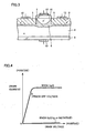
- FIG 3 is a diagram showing a pinch-off occurring and how a depletion layer 6 is formed in drift region 4 that is a low impurity concentration region of a pn junction portion. The electron flow is inhibited by depletion layer 6 and the drain current becomes saturated.
- Fig. 4 is a diagram representing a relation between the drain current and the drain voltage.
- the drain current increases linearly.
- the drain voltage reaches the pinch-off voltage, however, a depletion layer would grow from pn junction portions on either side of the drift region toward the drift region side as described above, thereby pinching off the drift region and causing saturation of the drain current.
- the gradient of the rise of the drain current is great in comparison with the conventional JFET.
- Fig. 4 also shows the off-state in which the drain current hardly flows in the case where a voltage lower than Vgoff (negative) is applied as the gate voltage (it is never made lower than Vgoff by more than a certain value, however).
- a reverse bias voltage is applied to gate electrode 12 to cause a depletion layer to be projected to channel region 10 from a pn junction interface between channel region 10 and confining region 5.
- the off-state is realized when the depletion layer blocks the cross section of a path toward the other surface in the channel region.
- depletion layer 6 is generated at a pn junction interface between confining region 5 and drift region 4 and becomes projected toward the drift region of a low concentration. This depletion layer withstands the voltage so that the withstand voltage performance of the device improves.
- the ON-OFF control is performed by the presence/absence of formation of the above-described depletion layer in the field effect transistor of the present invention. As a result, it has become possible to perform the control of high voltage and high current with certainty with the field effect transistor of the present invention.
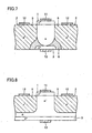
- depletion layer 6 When a high voltage is applied to a drain while the current is shut off in the off-state, depletion layer 6 is formed in a pn junction portion that is an interface between confining region 5 and drift region 4 close to a drain region, as shown in Fig. 5. Since this depletion layer 6 withstands the voltage between the drain and the gate, a field effect transistor with excellent withstand voltage can be achieved. This depletion layer 6 is formed toward a low impurity concentration side, with the depth being greater where the impurity concentration is lower, in a manner similar to the mechanism by which the above-described depletion layer is formed. As shown in Fig. 5, depletion layer 6 still has room for growth on the drain side even when the voltage is further increased from the state of Fig. 5 so that an extremely high voltage can be endured.
- drain region 3 is given a structure of being spread on a surface as shown in Fig. 1, drain region 3 may be confined and be given a structure in which drift region 4 above the drain region is also covered by confining region 5, as shown in Fig. 6.
- confining region 5 As shown in Fig. 6.
- depletion layer 6 that withstand the high voltage is formed as shown in Fig. 7.
- the scope of the present invention also includes a structure shown in Fig. 8 in which a thickness of the confining region is increased and drain region 3 and drift region 4 are given the structure of being spread on a surface as shown in Fig. 1.
- a thickness of drift region 4 sandwiched by the confining region and the drain region becomes thin so that a significant improvement in the withstand voltage cannot be expected; however, the thickness of the confining regions sandwiching the channel region is thick so that a normally-off JFET can be formed with ease.
- a method of manufacturing the JFET shown in Fig. 1 will be described.
- source region 1 other portions are etched and removed by RIE (Reactive Ion Etching).
- RIE Reactive Ion Etching
- p type impurity ions are implanted to form gate region 2 and confining region 5.
- Ni is formed as an electrode, and the JFET as shown in Fig. 1 is completed.
- the electrodes in the first embodiment, including the gate electrode are provided such that an ohmic contact is formed. Since the impurity concentration of gate region 2 is high, the formation of the ohmic contact is easy.
- the manufacturing steps are simplified, and the number of masks is reduced. Moreover, the chance of mask misalignment occurring reduces as well so that the yield can be improved.
- a semiconductor thin body and a semiconductor layer formed thereon were all formed by 4H-SiC, and withstand voltage performance and on-resistance (resistance in the on-state) of a JFET having the following dimensions were measured (with respect to a drift region thickness t 1 , a confining region thickness t 2 , a channel region width W, see Fig. 1).
- Fig. 12 is a cross sectional view of an arrangement of a JFET according to the second embodiment of the present invention.
- a source electrode 11 and a gate electrode 12 are provided on one main surface (front face) of a semiconductor substrate, while a drain electrode 13 is provided on the other main surface (reverse face).
- a source region 1 is formed in contact with source electrode 11, a gate region 2 is formed in contact with gate electrode 12, and a drain region 3 is formed in contact with drain electrode 13, respectively.
- Channel region 10 is provided in contact with source region 1 and gate region 2 and controls an on-state and an off-state of carriers by potentials of the gate region and the source region.
- a drift region 4 becomes a passage of electrons that are the carriers headed from channel region 10 to drain region 3.
- a width of drift region 4 may be confined by a confining region 5 of a p type conductive region, or may not be confined by confining region 5 as shown in Fig. 12.
- This JFET employed in a power semiconductor device is used to facilitate increasing and decreasing of the voltage and the like by providing a direct current in a pulsed manner by performing the switching of ON-OFF.
- a significant characteristic that the JFET for power semiconductor device of Fig. 12 has is that it is provided with an interposed region 20 that is in contact with source electrode 11 and that penetrates through source region 1 and protrudes into channel region 10.
- an n type semiconductor layer 32 is formed on an n + type semiconductor substrate 31.
- a mask 45 is formed on a region where a conductive layer is to be formed, and ion implantation of an n type impurity to a high concentration is effected on either side of the mask to form an n + layer.
- the above-described mask is removed and a mask 46 is newly formed on the n + layer on either side, ion implantation of a p type impurity to a high concentration is effected to form a p + type conductive layer.
- This p + type impurity region becomes interposed region 20 as shown in Fig. 16.
- source region 1 other portions are etched and removed by RIE (Reactive Ion Etching).
- RIE Reactive Ion Etching
- p type impurity ions are implanted to form gate region 2.
- Ni is formed as an electrode, and the power semiconductor device shown in Fig. 12 is completed.
- the electrodes in the second embodiment, including the gate electrode, are provided such that an ohmic contact is formed. Since an impurity concentration of each region is high, the formation of the ohmic contact is easy.
- a depletion layer is formed when a reverse bias voltage is applied between source electrode 11 and gate electrode 12 to cause the off-state.
- a reverse bias voltage is applied to an interface of a gate region and a channel region.
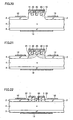
- a depletion layer grows on channel region 10 side having a low impurity concentration. Due to the presence of interposed region 20 of the p conductivity type that makes contact with gate electrode 12, this depletion layer 21 easily expands and expands to the source electrode side with a low voltage, as shown in Fig. 19.
- two depletion layers 21 that stretch out from either side of the channel region combine around the center of the width of channel region 10 at a tip portion of interposed region 20 and form a barrier against electrons.
- the electrons sense a potential barrier at a boundary portion of a p type conductive region so that it is not requisite that the depletion layers are combined, and the movement of electrons can be interrupted by interposed region 20 making contact with depletion layer 21.
- the off-state can be realized with a negative voltage whose absolute value is smaller than that in a conventional example, and it becomes possible to achieve an even lower loss as a power switching device.
- the semiconductor substrate used for the JFET shown in Fig. 12 is an SiC substrate having formed thereon an SiC layer by increasing the thickness by crystal growth.
- a material of the semiconductor substrate is not limited to SiC, and Si, GaAs and the like may be used.
- Fig. 20 is a cross sectional view showing a JFET used as a power semiconductor device in the third embodiment of the present invention.
- a significant difference between this device and the power semiconductor device of the second embodiment is that a plurality of interposed regions 20 are provided.
- a method of manufacturing the semiconductor device shown in Fig. 20 is basically the same as the method described in the second embodiment.
- a reverse bias voltage is applied between a source electrode and a gate electrode, due to the presence of interposed regions 20, a depletion layer 21 readily stretches out toward interposed regions 20 of the source region by a reverse bias voltage that is lower than that of the conventional example, as shown in Fig. 21.
- the off-state can be realized with a voltage lower than that of the conventional example, and it becomes possible to achieve an even lower loss as a power switching device.
- an n - layer 22 (low impurity concentration region) having a low impurity concentration is disposed making contact with a gate region 2 to facilitate the formation of a depletion layer that expands toward channel region 10 (Fig. 22).
- a tip portion of an interposed region 20 stretches out beyond a side of the gate region to a position reaching a drift region.
- Fig. 24 is a cross sectional view showing a JFET according to the fifth embodiment of the present invention.
- an n type impurity region on an n type SiC substrate has an impurity concentration that is determined by a device voltage resistance, and also serves as a first semiconductor layer of a first conductivity type (n type).
- an aluminum film 7 is formed filling a groove to a prescribed height.
- An n type SiC film forming channel regions 10a and 10b is formed on either side of aluminum film 7. A height of channel regions 10a and 10b is set a little higher than a height of the above-described aluminum film 7.
- p type SiC film 2a and 2b is formed on the outer side, and gate electrodes 12 are disposed thereon.
- source regions 1a and 1b are respectively formed, and source electrodes 11a and 11b are disposed thereon.
- n type SiC substrate 15 On the reverse face of n type SiC substrate 15, an n + type SiC film 3 is formed, and a drain electrode 13 is disposed thereon. Needless to say, an ohmic contact is formed between each electrode and a semiconductor layer.
- a negative voltage whose absolute value is large (-15 to -25 V) is applied to a gate, and consequently, reverse bias voltages are applied to the junction portions between channel regions 10a and 10b and the p type regions on the outer side thereof.
- a depletion layer width expands mainly toward the side on which the impurity concentration is low.
- the height of aluminum film 7 is set to be lower than channel regions 10a and 10b so that the path via the aluminum film is also shut off, and the off-state is realized.
- the vertical JFET shown in Fig. 24 has high withstand performance so that, by employing the JFET of the present embodiment, it becomes possible to provide a high voltage power device having small characteristic variation at each devices.
- a JFET according to the present invention can perform a high current, high voltage switching operation with a lower loss than in the conventional example. Moreover, by providing an interposed region that makes contact with a source electrode and that expands to a channel region, an off-state can be realized with a reverse bias voltage whose absolute value is smaller than that of the conventional example, and it becomes possible to provide a power semiconductor device of an even lower loss as a bulk power switching device. Furthermore, by providing a conductive layer in parallel to the channel region, the on-resistance can be brought to a low level, and the variation at each devices of the JFET can be reduced.
Landscapes
- Junction Field-Effect Transistors (AREA)
Abstract
Description
Claims (17)
- A junction field effect transistor, comprising:a gate region of a second conductivity type provided on one main surface of a semiconductor thin body;a source region of a first conductivity type provided on said one main surface side;a channel region of the first conductivity type that adjoins said source region;a confining region of the second conductivity type that adjoins said gate region and encloses and confines a range of said channel region;a drain region of the first conductivity type provided on other main surface of said semiconductor thin body; anda drift region of the first conductivity type that continuously lies in a direction of thickness of said semiconductor thin body from said channel region to said drain region, whereina concentration of an impurity of the first conductivity type in said drift region and said channel region is lower than a concentration of an impurity of the first conductivity type in said source region and the drain region and a concentration of an impurity of the second conductivity type in said confining region.
- The junction field effect transistor according to claim 1, wherein said confining region confines and encloses said gate region from an inner side of said semiconductor thin body.
- The junction field effect transistor according to claim 1, wherein said gate region coincides with said confining region.
- The junction field effect transistor according to claim 1, wherein said source region is formed protruding from the one main surface and said channel region is formed beneath said source region in a continuous manner.
- The junction field effect transistor according to claim 1, wherein said gate region is formed of two regions, the two gate regions being respectively confined and enclosed by confining regions, and said channel region is disposed in contact with and between the two confining regions.
- The junction field effect transistor according to claim 1, wherein a width of the channel region sandwiched by confining regions is smaller than a thickness of a depletion layer due to a built-in potential in a junction portion between said confining region and the channel region.
- The junction field effect transistor according to claim 1, wherein a first conductivity type impurity concentration of said drift region is higher than a first conductivity type impurity concentration of said channel region.
- The junction field effect transistor according to claim 1, comprising an interposed region of the second conductivity type that makes contact with a source electrode located on said source region and that passes through said source region and stretches out to said channel region.
- The junction field effect transistor according to claim 8, wherein said interposed region is separated into at least two regions with a region of the first conductivity type sandwiched therebetween.
- The junction field effect transistor according to claim 8, comprising a low impurity concentration region of the first conductivity type which is a region, within said channel region, in contact with said confining region and said source region and which has a concentration lower than a concentration of an impurity of the first conductivity type in said channel region.
- The junction field effect transistor according to claim 1, wherein said source region and the channel region are both separated into two regions, said junction field effect transistor comprising a conductive film sandwiched between the two channel regions in a position range that is lower than a top surface level of the channel region.
- The junction field effect transistor according to claim 11, wherein said conductive film extends into said drift region.
- The junction field effect transistor according to claim 11, wherein a channel region width from said confining region to a conductive film in said channel region is smaller than a depletion layer width in said channel region due to a built-in potential in a junction portion between said confining region and said channel region.
- The junction field effect transistor according to claim 11, wherein said conductive film is one of semiconductor films including a metal film and an impurity of high concentration.
- The junction field effect transistor according to claim 1, wherein said semiconductor thin body is an SiC substrate, and a first conductivity type semiconductor film is a first conductivity type SiC film, and a second conductivity type semiconductor film is a second conductivity type SiC film.
- A method of manufacturing a junction field effect transistor comprising the steps of:forming a first semiconductor layer of a first conductivity type of a concentration C1 that is lower than a concentration Cs on a semiconductor substrate of the first conductivity type including a first conductivity type impurity of said concentration Cs (a semiconductor substrate of the first conductivity type of concentration Cs);forming a second semiconductor layer of the first conductivity type of a concentration C2 that is lower than said concentrations Cs and C1 on said first semiconductor layer of the first conductivity type;forming a third semiconductor layer of the first conductivity type of a concentration C3 that is higher than said concentrations C1 and C2 on said second semiconductor layer of the first conductivity type;providing a mask for shielding a source region on said third semiconductor layer of the first conductivity type and removing said third semiconductor layer of the first conductivity type other than said source region by etching; anddoping said second semiconductor layer of the first conductivity type on either side of said source region with a second conductivity type impurity to form a second conductivity type confining region and a second conductivity type gate region of a concentration C4 that is higher than said concentration C2.
- The method of manufacturing a junction field effect transistor according to claim 16, wherein ion implantation in said second conductivity type impurity doping is performed using a same mask used for etching of said third semiconductor layer of the first conductivity type.
Priority Applications (2)
| Application Number | Priority Date | Filing Date | Title |
|---|---|---|---|
| EP09006349A EP2081218B1 (en) | 1999-12-24 | 2000-09-11 | Junction field effect transistor |
| EP09006462A EP2081219B1 (en) | 1999-12-24 | 2000-09-11 | Junction field effect transistor |
Applications Claiming Priority (7)
| Application Number | Priority Date | Filing Date | Title |
|---|---|---|---|
| JP11366799A JP2000299475A (en) | 1999-02-12 | 1999-12-24 | Field effect transistor and method of manufacturing the same |
| JP36679999 | 1999-12-24 | ||
| JP2000008969 | 2000-01-18 | ||
| JP2000008969A JP4876297B2 (en) | 2000-01-18 | 2000-01-18 | Power semiconductor device |
| JP2000194464 | 2000-06-28 | ||
| JP2000194464A JP4830179B2 (en) | 2000-06-28 | 2000-06-28 | Junction field effect transistor |
| PCT/JP2000/006211 WO2001048809A1 (en) | 1999-12-24 | 2000-09-11 | Junction field-effect transistor and method of manufacture thereof |
Related Child Applications (4)
| Application Number | Title | Priority Date | Filing Date |
|---|---|---|---|
| EP09006349A Division EP2081218B1 (en) | 1999-12-24 | 2000-09-11 | Junction field effect transistor |
| EP09006462A Division EP2081219B1 (en) | 1999-12-24 | 2000-09-11 | Junction field effect transistor |
| EP09006349.6 Division-Into | 2009-05-11 | ||
| EP09006462.7 Division-Into | 2009-05-13 |
Publications (3)
| Publication Number | Publication Date |
|---|---|
| EP1284496A1 true EP1284496A1 (en) | 2003-02-19 |
| EP1284496A4 EP1284496A4 (en) | 2007-06-27 |
| EP1284496B1 EP1284496B1 (en) | 2010-11-17 |
Family
ID=27341738
Family Applications (3)
| Application Number | Title | Priority Date | Filing Date |
|---|---|---|---|
| EP00957106A Expired - Lifetime EP1284496B1 (en) | 1999-12-24 | 2000-09-11 | Junction field-effect transistor and method of manufacture thereof |
| EP09006462A Expired - Lifetime EP2081219B1 (en) | 1999-12-24 | 2000-09-11 | Junction field effect transistor |
| EP09006349A Expired - Lifetime EP2081218B1 (en) | 1999-12-24 | 2000-09-11 | Junction field effect transistor |
Family Applications After (2)
| Application Number | Title | Priority Date | Filing Date |
|---|---|---|---|
| EP09006462A Expired - Lifetime EP2081219B1 (en) | 1999-12-24 | 2000-09-11 | Junction field effect transistor |
| EP09006349A Expired - Lifetime EP2081218B1 (en) | 1999-12-24 | 2000-09-11 | Junction field effect transistor |
Country Status (8)
| Country | Link |
|---|---|
| US (1) | US6870189B1 (en) |
| EP (3) | EP1284496B1 (en) |
| KR (1) | KR100661691B1 (en) |
| CN (1) | CN1243373C (en) |
| CA (1) | CA2395608C (en) |
| DE (2) | DE60045260D1 (en) |
| TW (1) | TW456042B (en) |
| WO (1) | WO2001048809A1 (en) |
Cited By (2)
| Publication number | Priority date | Publication date | Assignee | Title |
|---|---|---|---|---|
| EP1825522A4 (en) * | 2004-12-01 | 2009-04-01 | Semisouth Lab Inc | SIDE PITCH FIELD EFFECT TRANSISTORS IN HABITAT MATERIALS WITH WIDE BAND DISTANCE, METHOD OF MANUFACTURING THEM AND INTEGRATED CIRCUITS WITH THE TRANSISTORS |
| WO2018048972A1 (en) | 2016-09-09 | 2018-03-15 | United Silicon Carbide Inc. | Trench vertical jfet with improved threshold voltage control |
Families Citing this family (21)
| Publication number | Priority date | Publication date | Assignee | Title |
|---|---|---|---|---|
| ATE535010T1 (en) * | 2001-07-12 | 2011-12-15 | Univ Mississippi State | METHOD FOR PRODUCING SELF-ALIGNED TRANSISTOR TOPOLOGIES IN SILICON CARBIDE BY USING SELECTIVE EPITAXY |
| KR100477396B1 (en) * | 2002-09-04 | 2005-03-28 | 한국전기연구원 | SiC MOSFET devices having metal gate electrode and manufacturing method thereof |
| US7417270B2 (en) * | 2004-06-23 | 2008-08-26 | Texas Instruments Incorporated | Distributed high voltage JFET |
| US7569873B2 (en) * | 2005-10-28 | 2009-08-04 | Dsm Solutions, Inc. | Integrated circuit using complementary junction field effect transistor and MOS transistor in silicon and silicon alloys |
| US7863656B2 (en) * | 2006-05-12 | 2011-01-04 | Cree Sweden Ab | Semiconductor device |
| US7763506B2 (en) * | 2007-09-10 | 2010-07-27 | Infineon Technologies Austria Ag | Method for making an integrated circuit including vertical junction field effect transistors |
| US7977713B2 (en) * | 2008-05-08 | 2011-07-12 | Semisouth Laboratories, Inc. | Semiconductor devices with non-punch-through semiconductor channels having enhanced conduction and methods of making |
| US7994548B2 (en) * | 2008-05-08 | 2011-08-09 | Semisouth Laboratories, Inc. | Semiconductor devices with non-punch-through semiconductor channels having enhanced conduction and methods of making |
| JP5452062B2 (en) * | 2009-04-08 | 2014-03-26 | 三菱電機株式会社 | Method for manufacturing silicon carbide semiconductor device |
| TWI405332B (en) | 2010-03-10 | 2013-08-11 | Macronix Int Co Ltd | Junction field effect transistor component |
| US9184305B2 (en) * | 2011-08-04 | 2015-11-10 | Avogy, Inc. | Method and system for a GAN vertical JFET utilizing a regrown gate |
| US8969912B2 (en) | 2011-08-04 | 2015-03-03 | Avogy, Inc. | Method and system for a GaN vertical JFET utilizing a regrown channel |
| US9112048B2 (en) * | 2011-08-17 | 2015-08-18 | Ramgoss Inc. | Vertical field effect transistor on oxide semiconductor substrate |
| US9006800B2 (en) | 2011-12-14 | 2015-04-14 | Avogy, Inc. | Ingan ohmic source contacts for vertical power devices |
| CN103730517A (en) * | 2012-10-15 | 2014-04-16 | 上海华虹宏力半导体制造有限公司 | Junction field effect transistor and manufacturing method thereof |
| JP6787367B2 (en) | 2017-07-26 | 2020-11-18 | 株式会社デンソー | Semiconductor device |
| US10361127B1 (en) | 2017-12-28 | 2019-07-23 | International Business Machines Corporation | Vertical transport FET with two or more gate lengths |
| JP2019175908A (en) * | 2018-03-27 | 2019-10-10 | トヨタ自動車株式会社 | Semiconductor device and method for manufacturing the same |
| JP6973422B2 (en) | 2019-01-21 | 2021-11-24 | 株式会社デンソー | Manufacturing method of semiconductor device |
| JP6950714B2 (en) | 2019-01-21 | 2021-10-13 | 株式会社デンソー | Semiconductor device |
| WO2026049789A1 (en) * | 2024-08-26 | 2026-03-05 | Microchip Technology Incorporated | Transistor and method for manufacturing same |
Family Cites Families (8)
| Publication number | Priority date | Publication date | Assignee | Title |
|---|---|---|---|---|
| JPS5378177A (en) * | 1976-12-22 | 1978-07-11 | Toshiba Corp | Field effect transistor |
| JPS5846874B2 (en) * | 1977-04-27 | 1983-10-19 | 三菱電機株式会社 | Junction field effect transistor |
| JPH04273169A (en) * | 1991-02-28 | 1992-09-29 | Fuji Electric Co Ltd | Electrostatic induction transistor |
| JP2689057B2 (en) * | 1992-09-16 | 1997-12-10 | 本田技研工業株式会社 | Static induction semiconductor device |
| US5396085A (en) * | 1993-12-28 | 1995-03-07 | North Carolina State University | Silicon carbide switching device with rectifying-gate |
| US5903020A (en) * | 1997-06-18 | 1999-05-11 | Northrop Grumman Corporation | Silicon carbide static induction transistor structure |
| US5945701A (en) * | 1997-12-19 | 1999-08-31 | Northrop Grumman Corporation | Static induction transistor |
| US6313482B1 (en) * | 1999-05-17 | 2001-11-06 | North Carolina State University | Silicon carbide power devices having trench-based silicon carbide charge coupling regions therein |
-
2000
- 2000-09-11 DE DE60045260T patent/DE60045260D1/en not_active Expired - Lifetime
- 2000-09-11 WO PCT/JP2000/006211 patent/WO2001048809A1/en not_active Ceased
- 2000-09-11 CA CA2395608A patent/CA2395608C/en not_active Expired - Fee Related
- 2000-09-11 TW TW089118554A patent/TW456042B/en not_active IP Right Cessation
- 2000-09-11 EP EP00957106A patent/EP1284496B1/en not_active Expired - Lifetime
- 2000-09-11 CN CNB008183619A patent/CN1243373C/en not_active Expired - Fee Related
- 2000-09-11 KR KR1020027008192A patent/KR100661691B1/en not_active Expired - Fee Related
- 2000-09-11 EP EP09006462A patent/EP2081219B1/en not_active Expired - Lifetime
- 2000-09-11 US US10/168,265 patent/US6870189B1/en not_active Expired - Fee Related
- 2000-09-11 EP EP09006349A patent/EP2081218B1/en not_active Expired - Lifetime
- 2000-09-11 DE DE60045497T patent/DE60045497D1/en not_active Expired - Lifetime
Cited By (4)
| Publication number | Priority date | Publication date | Assignee | Title |
|---|---|---|---|---|
| EP1825522A4 (en) * | 2004-12-01 | 2009-04-01 | Semisouth Lab Inc | SIDE PITCH FIELD EFFECT TRANSISTORS IN HABITAT MATERIALS WITH WIDE BAND DISTANCE, METHOD OF MANUFACTURING THEM AND INTEGRATED CIRCUITS WITH THE TRANSISTORS |
| WO2018048972A1 (en) | 2016-09-09 | 2018-03-15 | United Silicon Carbide Inc. | Trench vertical jfet with improved threshold voltage control |
| EP3510637A4 (en) * | 2016-09-09 | 2020-04-15 | United Silicon Carbide Inc. | VERTICAL TRENCH JFET WITH IMPROVED THRESHOLD VOLTAGE CONTROL |
| EP4598298A3 (en) * | 2016-09-09 | 2025-10-22 | United Silicon Carbide Inc. | Trench vertical jfet with improved threshold voltage control |
Also Published As
| Publication number | Publication date |
|---|---|
| EP1284496A4 (en) | 2007-06-27 |
| KR20020062989A (en) | 2002-07-31 |
| DE60045497D1 (en) | 2011-02-17 |
| CA2395608A1 (en) | 2001-07-05 |
| CN1423836A (en) | 2003-06-11 |
| EP2081219A1 (en) | 2009-07-22 |
| TW456042B (en) | 2001-09-21 |
| US6870189B1 (en) | 2005-03-22 |
| KR100661691B1 (en) | 2006-12-26 |
| EP2081218B1 (en) | 2011-11-09 |
| WO2001048809A1 (en) | 2001-07-05 |
| EP2081218A1 (en) | 2009-07-22 |
| EP2081219B1 (en) | 2011-01-05 |
| CN1243373C (en) | 2006-02-22 |
| CA2395608C (en) | 2010-06-22 |
| EP1284496B1 (en) | 2010-11-17 |
| DE60045260D1 (en) | 2010-12-30 |
Similar Documents
| Publication | Publication Date | Title |
|---|---|---|
| US6870189B1 (en) | Pinch-off type vertical junction field effect transistor and method of manufacturing the same | |
| US5087581A (en) | Method of forming vertical FET device with low gate to source overlap capacitance | |
| JP2606404B2 (en) | Semiconductor device | |
| US7728336B2 (en) | Silicon carbide semiconductor device and method for producing the same | |
| US6258674B1 (en) | High voltage field effect transistor and method of fabricating the same | |
| US5073519A (en) | Method of fabricating a vertical FET device with low gate to drain overlap capacitance | |
| CN101036231A (en) | Enhanced RESURF HVPMOS device with stacked hetero-doping rim and gradual drift region | |
| DE10036208A1 (en) | Semiconductor structure with buried island area and contact area | |
| US20060027863A1 (en) | Semiconductor device and method of manufacturing the same | |
| US5844273A (en) | Vertical semiconductor device and method of manufacturing the same | |
| KR100256387B1 (en) | A lateral insulated gate field effect semiconductor device | |
| KR20010051995A (en) | Emitter ballast resistor with enhanced body effect to improve the short circuit withstand capability of power devices | |
| US6268626B1 (en) | DMOS field effect transistor with improved electrical characteristics and method for manufacturing the same | |
| US7256453B2 (en) | Semiconductor device | |
| JP4127987B2 (en) | Semiconductor device | |
| KR100290913B1 (en) | High voltage devicd and method for manufacturing the same | |
| JPH0237777A (en) | vertical field effect transistor | |
| US20030107087A1 (en) | Dual gate oxide high-voltage semiconductor device | |
| JP2000299475A (en) | Field effect transistor and method of manufacturing the same | |
| JP3189543B2 (en) | Semiconductor device | |
| JP4876297B2 (en) | Power semiconductor device | |
| JP3279092B2 (en) | Semiconductor device | |
| JP2026059629A (en) | Switching element | |
| JPS61168254A (en) | High withstand voltage mos field effect semiconductor device | |
| WO2025026540A1 (en) | Semiconductor device, method for operating a semiconductor device and method for producing a semiconductor device |
Legal Events
| Date | Code | Title | Description |
|---|---|---|---|
| PUAI | Public reference made under article 153(3) epc to a published international application that has entered the european phase |
Free format text: ORIGINAL CODE: 0009012 |
|
| 17P | Request for examination filed |
Effective date: 20020723 |
|
| AK | Designated contracting states |
Designated state(s): AT BE CH CY DE DK ES FI FR GB GR IE IT LI LU MC NL PT SE |
|
| RBV | Designated contracting states (corrected) |
Designated state(s): AT BE CH CY DE FR GB LI SE |
|
| A4 | Supplementary search report drawn up and despatched |
Effective date: 20070525 |
|
| 17Q | First examination report despatched |
Effective date: 20070830 |
|
| RBV | Designated contracting states (corrected) |
Designated state(s): CH DE FR GB LI SE |
|
| GRAP | Despatch of communication of intention to grant a patent |
Free format text: ORIGINAL CODE: EPIDOSNIGR1 |
|
| GRAS | Grant fee paid |
Free format text: ORIGINAL CODE: EPIDOSNIGR3 |
|
| GRAA | (expected) grant |
Free format text: ORIGINAL CODE: 0009210 |
|
| AK | Designated contracting states |
Kind code of ref document: B1 Designated state(s): CH DE FR GB LI SE |
|
| REG | Reference to a national code |
Ref country code: GB Ref legal event code: FG4D |
|
| REG | Reference to a national code |
Ref country code: CH Ref legal event code: EP Ref country code: CH Ref legal event code: NV Representative=s name: BOVARD AG PATENTANWAELTE |
|
| REF | Corresponds to: |
Ref document number: 60045260 Country of ref document: DE Date of ref document: 20101230 Kind code of ref document: P |
|
| REG | Reference to a national code |
Ref country code: SE Ref legal event code: TRGR |
|
| REG | Reference to a national code |
Ref country code: CH Ref legal event code: PFA Owner name: SUMITOMO ELECTRIC INDUSTRIES, LTD. Free format text: SUMITOMO ELECTRIC INDUSTRIES, LTD.#5-33, KITAHAMA 4-CHOME CHUO-KU#OSAKA-SHI, OSAKA 541-0041 (JP) -TRANSFER TO- SUMITOMO ELECTRIC INDUSTRIES, LTD.#5-33, KITAHAMA 4-CHOME CHUO-KU#OSAKA-SHI, OSAKA 541-0041 (JP) |
|
| PLBE | No opposition filed within time limit |
Free format text: ORIGINAL CODE: 0009261 |
|
| STAA | Information on the status of an ep patent application or granted ep patent |
Free format text: STATUS: NO OPPOSITION FILED WITHIN TIME LIMIT |
|
| 26N | No opposition filed |
Effective date: 20110818 |
|
| PGFP | Annual fee paid to national office [announced via postgrant information from national office to epo] |
Ref country code: CH Payment date: 20110913 Year of fee payment: 12 |
|
| PGFP | Annual fee paid to national office [announced via postgrant information from national office to epo] |
Ref country code: SE Payment date: 20110913 Year of fee payment: 12 Ref country code: GB Payment date: 20110907 Year of fee payment: 12 Ref country code: DE Payment date: 20110907 Year of fee payment: 12 Ref country code: FR Payment date: 20110922 Year of fee payment: 12 |
|
| REG | Reference to a national code |
Ref country code: DE Ref legal event code: R097 Ref document number: 60045260 Country of ref document: DE Effective date: 20110818 |
|
| PG25 | Lapsed in a contracting state [announced via postgrant information from national office to epo] |
Ref country code: SE Free format text: LAPSE BECAUSE OF NON-PAYMENT OF DUE FEES Effective date: 20120912 |
|
| REG | Reference to a national code |
Ref country code: CH Ref legal event code: PL Ref country code: SE Ref legal event code: EUG |
|
| GBPC | Gb: european patent ceased through non-payment of renewal fee |
Effective date: 20120911 |
|
| REG | Reference to a national code |
Ref country code: FR Ref legal event code: ST Effective date: 20130531 |
|
| REG | Reference to a national code |
Ref country code: DE Ref legal event code: R119 Ref document number: 60045260 Country of ref document: DE Effective date: 20130403 |
|
| PG25 | Lapsed in a contracting state [announced via postgrant information from national office to epo] |
Ref country code: GB Free format text: LAPSE BECAUSE OF NON-PAYMENT OF DUE FEES Effective date: 20120911 Ref country code: CH Free format text: LAPSE BECAUSE OF NON-PAYMENT OF DUE FEES Effective date: 20120930 Ref country code: LI Free format text: LAPSE BECAUSE OF NON-PAYMENT OF DUE FEES Effective date: 20120930 Ref country code: DE Free format text: LAPSE BECAUSE OF NON-PAYMENT OF DUE FEES Effective date: 20130403 |
|
| PG25 | Lapsed in a contracting state [announced via postgrant information from national office to epo] |
Ref country code: FR Free format text: LAPSE BECAUSE OF NON-PAYMENT OF DUE FEES Effective date: 20121001 |