EP1283597A2 - Clock producing circuit capable of suppressing phase shift at a time of change from active clock to standby clock - Google Patents
Clock producing circuit capable of suppressing phase shift at a time of change from active clock to standby clock Download PDFInfo
- Publication number
- EP1283597A2 EP1283597A2 EP02017661A EP02017661A EP1283597A2 EP 1283597 A2 EP1283597 A2 EP 1283597A2 EP 02017661 A EP02017661 A EP 02017661A EP 02017661 A EP02017661 A EP 02017661A EP 1283597 A2 EP1283597 A2 EP 1283597A2
- Authority
- EP
- European Patent Office
- Prior art keywords
- clock
- phase
- output
- output clock
- signal
- Prior art date
- Legal status (The legal status is an assumption and is not a legal conclusion. Google has not performed a legal analysis and makes no representation as to the accuracy of the status listed.)
- Granted
Links
Images



Classifications
-
- H—ELECTRICITY
- H03—ELECTRONIC CIRCUITRY
- H03L—AUTOMATIC CONTROL, STARTING, SYNCHRONISATION OR STABILISATION OF GENERATORS OF ELECTRONIC OSCILLATIONS OR PULSES
- H03L7/00—Automatic control of frequency or phase; Synchronisation
- H03L7/06—Automatic control of frequency or phase; Synchronisation using a reference signal applied to a frequency- or phase-locked loop
- H03L7/08—Details of the phase-locked loop
- H03L7/085—Details of the phase-locked loop concerning mainly the frequency- or phase-detection arrangement including the filtering or amplification of its output signal
- H03L7/093—Details of the phase-locked loop concerning mainly the frequency- or phase-detection arrangement including the filtering or amplification of its output signal using special filtering or amplification characteristics in the loop
-
- H—ELECTRICITY
- H03—ELECTRONIC CIRCUITRY
- H03L—AUTOMATIC CONTROL, STARTING, SYNCHRONISATION OR STABILISATION OF GENERATORS OF ELECTRONIC OSCILLATIONS OR PULSES
- H03L7/00—Automatic control of frequency or phase; Synchronisation
- H03L7/06—Automatic control of frequency or phase; Synchronisation using a reference signal applied to a frequency- or phase-locked loop
- H03L7/07—Automatic control of frequency or phase; Synchronisation using a reference signal applied to a frequency- or phase-locked loop using several loops, e.g. for redundant clock signal generation
Definitions
- This invention relates to a clock producing circuit receiving active and standby clocks, in particular, to a clock producing circuit which is capable of suppressing a phase shift at the time of a change from an active reference clock to a standby reference clock.
- active and standby reference clocks are supplied to a synchronous clock producing circuit used in a synchronous timing control system for an apparatus that high reliability is required. According to such structure, even if the active reference clock disappears (or comes into an abnormal state), the synchronous clock producing circuit is still able to produce an output clock by using the standby reference clock instead of the active reference clock. Thus the synchronous clock producing circuit can supply the output clock to the apparatus even if it can not receive the active reference clock.
- the standby reference clock does not always correspond to the active reference clock in phase. If the change from the active reference clock to the standby reference clock is performed under the condition that the phase of the standby reference clock does not correspond to that of the active reference clock, the output clock has a phase shift or change at the time of a change from the active reference clock to the standby reference clock.
- a clock producing circuit receives first and second reference clocks at first and second input terminals.
- the clock producing circuit comprises first phase locked loop connected to the first input terminal to receive the first reference clock and to produce a first output clock having first phase according to the first reference clock.
- a second phase locked loop has a digital filter with filter coefficients and is connected to the second input terminal to receive the second reference clock and to produce a second output clock having second phase according to the second reference clock.
- a comparing portion is connected to the first phase locked loop and the second phase locked loop to compare the first phase with the second phase and to supply a filter coefficient control signal representative of difference between the first phase and the second phase to the digital filter.
- the digital filter updates the filter coefficients according to the filter coefficient control signal so as to reduce the difference between the first phase and the second phase.
- a clock producing circuit has first and second phase locked loops to produce first and second output clocks according to first and second reference clocks.
- the clock producing circuit comprises a subsidiary phase comparator connected to the first and second phase locked loops to compare phase of the first output clock with that of the second output clock and to produce a subsidiary comparison signal representing phase difference between the first and second output clocks.
- a phase adjusting portion is included in the second phase locked loop and connected to the subsidiary phase comparator to adjust phase of the second output clock on the basis of the subsidiary comparison signal so that the phase of the second output clock coincides with that of the first output clock.
- a clock producing method comprising the steps of producing a first output clock according to a first reference clock by the use of a first phase locked loop, producing a second output clock according to a second reference clock by the use of a second phase locked loop, comparing phase of the first output clock with that of the second output clock to produce a comparison signal representing phase difference between the first and the second output clocks, and adjusting phase of the second output clock according to the comparison signal by the use of a digital filter included in the second phase locked loop so as to reduce said phase difference.
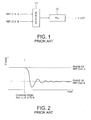
- the conventional synchronous clock producing circuit comprises a selector 11 and a phase locked loop (PLL) 12.
- the selector 11 receives two reference clocks A and B and selectively supplies one of them to the PLL 12.
- the PLL 12 produces an output clock synchronized with the reference clock A or B supplied from the selector 11.
- the selector 11 executes a change between the reference clocks A and B. For example, the selector 11 changes from the reference clock A to the reference clock B. Consequently, the PLL 12 produces the output clock synchronized with the reference clock B after the change from the reference clock A to the reference clock B.
- the reference clocks A and B coincides with (or corresponds to) each other in phase.
- the phase of the reference clock B does not always corresponds to that of the reference clock A.
- Phase difference between the reference clocks A and B causes a phase shift and/or sharp phase changes into the output clock at the time of the change between the reference clocks A and B.
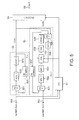
- Fig. 2 shows time variation of the phase of the output signal before and after the change between the reference clocks A and B.
- JP-A 9-64732 uses a holdover state of a digital filter included in a phase locked loop circuit.
- the lock producing circuit is shown in Fig. 3.
- the clock producing circuit comprises a selecting circuit 31, an input disappearance detecting circuit 32 and a phase locked loop (PLL) 33.
- PLL phase locked loop
- the PLL 33 comprises a phase comparator (PC) 331, an analog filter (AFIL) 332, an analog to digital converter (A/D) 333, a digital filter (DFIL) 334, a digital to analog converter (D/A) 335, a voltage controlled oscillator 336, and a dividing counter 337.
- PC phase comparator
- AFIL analog filter
- A/D analog to digital converter
- DFIL digital filter
- D/A digital to analog converter
- D/A digital to analog converter
- the selecting circuit 31 selects a reference clock A to supply it to the PLL 33.
- the input disappearance detecting circuit 32 demands that the digital filter 334 comes into the holdover state when it does not receive the reference clock A.
- the digital filter 334 reduces a loop gain of the PLL 33 in response to the demand from the input disappearance detecting circuit 32.
- the PLL 33 comes into the holdover state.
- the PLL 33 produces the output clock with a fixed phase.
- the input disappearance detecting circuit 32 further makes the selecting circuit 31 select a reference clock B.
- the selecting circuit 31 selects the reference clock B
- the input disappearance detecting circuit 32 demands that the digital filter 334 returns from the holdover state.
- the output clock is synchronized with the reference clock B.
- a next-stage PLL circuit (not shown) connected to an output terminal of the PLL 33 can follow the changes of the output clock.
- the clock producing circuit of Fig. 3 does not consider phase difference between the reference clocks A and B. That is, when there is phase difference between the reference clocks A and B and the change is performed between them, the phase shift occurs in the output clock as shown in Fig. 4.
- a phase adjusting circuit comprises two clock receiving panels having the same structure. One of the clock receiving panels is used for an active system while the other is used for a standby system.
- the active system produces not only a first output clock but also a timing signal according to a first reference signal.
- the standby system produces not only a second output clock but also a collation signal according to a second reference signal.
- the timing signal is supplied from the active system to the standby system.
- the standby system produces a phase control pulse when phase difference between the timing signal and the collation pulse is larger than a predetermined value.
- the phase control pulse is used for adjusting the phase of the second output clock.
- the phase adjusting circuit of P2000-2614220A can limit the phase difference between the first and the second output clocks to the predetermined value.
- this does not mean that the second output clock coincides with (or corresponds to) the first output clock in phase. That is, the phase difference is merely limited within the predetermined value.
- a phase control system comprises two clock receiving boards having the same structure.
- One of the clock receiving boards is used for a master board while the other is used for a slave board.
- the master board produces a master clock according to a first reference clock.
- the slave board produces not only a slave clock but also a window signal according to a second reference clock. Furthermore, the slave board adjusts phase of the slave clock so that each rising edge of the slave clock is within each high level period of the window signal.
- phase control system of JP-A 10-187272 can limit phase difference between the master and slave clocks to the high level period of the window signal.
- the phase of the slave clock does not always correspond to that of the master clock.
- Fig. 5 is a block diagram showing a structure of the clock producing circuit.
- the clock producing circuit comprises input terminals 501 and 502, a control unit (CNT) 51, a first phase locked loop (PLL1) 52, a second phase locked loop (PLL2) 53, a selector (SEL) 54, and an output terminal 55.
- CNT control unit
- PLL1 phase locked loop
- PLL2 phase locked loop
- SEL selector
- the clock producing circuit is supplied with first and second reference clocks A and B produced by two oscillators (not shown) via the input terminals 501 and 502.
- the first and second reference clocks A and B have the same frequency.
- the control unit 51 is connected to the first and second input terminals 501 and 502 and receives both of the first and second reference clocks A and B to produces a selecting signal.
- the control unit 51 serves as a monitor portion and monitors a state of the first and second reference clocks A and B.
- the selecting signal specifies the first reference clock A.
- the selecting signal specifies the second reference clock B.
- the selecting signal is supplied to the second PLL 53 and the selector 54.
- the first PLL 52 comprises a first phase comparator (PC1) 521, a first analog filter (AFIL1) 522, a first voltage controlled oscillator (VCXO1) 523 and a first dividing counter 524.
- the first phase comparator 521 receives the first reference clock A and a first feedback clock from the first dividing counter 524 to produce a first comparison signal representing phase difference between the first reference clock A and the first feedback clock.
- the first analog filter 522 receives the first comparison signal and filters it to produce a first filtered comparison signal as a first voltage control signal.
- the first VCXO 523 produces a first output clock (CLK1) according to the first voltage control signal.
- the first output clock CLK1 supplied to the selector 54, the second PLL 53 and the first dividing counter 524.
- the first dividing counter 524 counts pulses of the first output clock CLK1 to divide a frequency of the first output clock CLK1 and to produce the first feedback clock.
- the first dividing counter 524 has a fixed or a variable dividing ratio.
- the second PLL 53 comprises a second phase comparator (PC2) 531, a second analog filter (AFIL2) 532, a first analog to digital converter (A/D1) 533, a digital filter 534, a digital to analog converter (D/A) 535, a second voltage controlled oscillator 536, a second dividing counter 537, a third phase comparator (PC3) 538 and a second analog to digital converter (A/D2) 539.
- PC2 phase comparator (PC2) 531 PC2 phase comparator (PC2) 531
- AFIL2 second analog filter
- A/D1 first analog to digital converter
- D/A digital to analog converter
- PC3 second dividing counter
- PC3 third phase comparator
- A/D2 second analog to digital converter
- the second phase comparator 531 receives the second reference clock B and a second feedback clock supplied from the second dividing counter 537 and produces a second comparison signal representing phase difference between the second reference clock B and the second feedback clock.
- the second analog filter 532 filters the second comparison signal to produce a second filtered comparison signal.
- the first A/D converter 533 converts the second filtered comparison signal into a digital comparison signal.
- the digital filter 534 filters the digital comparison signal to produce a digital filtered signal (or a digital voltage control signal).
- the D/A converter converts the digital filtered signal into a second voltage control signal.
- the second VCXO 536 produces a second output clock (CLK2) according to the second voltage control signal.
- the second output clock CLK2 is supplied to the selector 54, the second dividing counter 537 and the third phase comparator 538.
- the second dividing counter 537 counts pulses of the second output clock CLK2 to divide a frequency of the second output clock CLK2 and to produce the second feedback clock.
- the second dividing counter 537 has a fixed or a variable dividing ratio.
- the third phase comparator 538 compares the first output clock CLK1 from the first PLL 52 with the second output clock CLK2 to produce a third comparison signal representing phase difference between the first output clock CLK1 and the second output clock CLK2.
- the second A/D comparator 539 converts the third comparison signal into a filter coefficient control signal.
- the third phase comparator 538 and the second A/D comparator 539 serves as a comparison portion to produce the filter coefficient control signal for controlling filter coefficients of the digital filter 534.
- the second phase comparator 531 serves as a principal phase comparator while the third phase comparator 538 serves as a subsidiary phase comparator.
- the selector 54 receives the first and the second output clocks CLK1 and CLK2 and the selecting signal and selects one of the output clocks CLK1 and CLK2 as a selected output clock according to the selecting signal.
- the selected output clock is supplied to the output terminal 55.
- the selector 54 serves as a selecting portion together with the control unit 51.
- the selector 54 selects the first output clock CLK1 produced by the first PLL 52 in the beginning and selects the second output clock CLK2 produced by the second PLL 53 later.
- a change from the first output clock CLK1 to the second output clock CLK2 is carried out when the first reference clock A disappears.
- the first phase comparator 521 Upon receiving the first reference clock A via the input terminal 501, the first phase comparator 521 compares the first reference clock A with the first feedback clock from the first dividing counter 524 to produce the first comparison signal.
- the first analog filter 522 averages the first comparison signal to produce a first averaged comparison signal as the first voltage control signal.
- the first VCXO 523 controls a frequency of the first output clock CLK1 according to the first voltage control signal.
- the first output clock CLK1 is supplied to the selector 54 as an output of the first PLL 52 and to the first dividing counter 524.
- the first dividing counter 524 divides the first output clock CLK1 so that divided clock has a frequency which is approximately equal to that of the first reference clock A.
- the divided clock is supplied to the first phase comparator 521 as the first feedback clock.
- the second phase comparator 531 compares the second reference clock B with the second feedback clock from the second dividing counter 537 to produce the second comparison signal.
- the second analog filter 532 averages the second comparison signal to produce a second averaged comparison signal as the second filtered comparison signal.
- the first A/D converter 533 converts the second averaged comparison signal into the digital comparison signal.
- the digital filter 534 controls filter coefficients thereof according to the filter coefficient control signal supplied from the second A/D converter 539.
- the filter coefficient control signal depends on the phase difference between the first and the second output clocks CLK1 and CLK2. Accordingly, the filter coefficients of the digital filter 534 are updated to reduce the phase difference between the first and second output clocks CLK1 and CLK2.
- a combination of the digital filter 534 and the second A/D converter 539 serves as a phase adjusting portion for adjusting the phase of the second output clock CLK2.
- the second output clock CLK2 substantially coincides with the first output clock CLK1.
- the digital filter 534 filters the digital comparison signal by the use of the filter coefficients decided by the filter coefficient control signal.
- the D/A converter 535 converts the digital filtered signal into the second voltage control signal.
- the second VCXO 536 controls a frequency of the second output clock CLK2 according to the second voltage control signal.
- the second output clock CLK2 is supplied to the selector 54 as an output of the second PLL 53 and to the second dividing counter 524 and to the third phase comparator 538.
- the second dividing counter 537 divides the second output clock CLK2 so that divided clock has a frequency which is approximately equal to that of the second reference clock B (or the first reference clock A) .
- the divided clock is supplied to the second phase comparator 531 as the second feedback clock.
- the digital filter 534 controls the filter coefficients thereof according to the output of the third phase comparator 538 so that no phase difference is made between the first and second output clocks CLK1 and CLK2.
- the second output clock CLK2 has a phase offset against the second reference clock B. Therefore, the second output clock CLK2 coincides with or corresponds to both of the first output clock CLK1 and the first reference clock A in phase .
- control unit 51 controls the selector 54 to select the first output clock CLK1, the clock producing circuit outputs the first output clock CLK1.
- the control unit 51 Upon detecting absence of the first reference clock A, the control unit 51 produces the selecting signal specifying the second output clock CLK2.
- the selecting signal specifying the second output clock CLK2 is supplied to the digital filter 534 and the selector 54.
- the digital filter 534 When the digital filter 534 receives the selecting signal specifying the second output clock CLK2, it stops controlling the filter coefficients and fixes the filter coefficients at the time. The digital filter 534 maintains the fixed filter coefficients while it receives the selecting signal specifying the second output clock CLK2.
- the selector 54 changes the selected output clock from the first output clock CLK1 to the second output clock CLK2.
- the second output clock CLK2 is synchronous with the first output clock CLK1.
- the second output clock CLK2 has the phase offset against the second reference clock B. That is, the second output clock CLK2 coincides with the first output clock CLK1. Therefore, when the selector 54 changes the selected output clock from the first output clock CLK1 to the second output clock CLK2, sharp phase shift does not occur in the selected output clock.
- the fixed filter coefficients of the digital filter 534 correspond to the phase difference between the first and second reference clocks A and B at the time of the change from the first output clock CLK1 to the second output clock CLK2. This can regard the second voltage controlled oscillator 536 as depending on the first reference clock A.
- Fig.6 shows time variation of the phase of the selected output clock before and after the change of the selected output clock from the first output clock CLK1 to the second output clock CLK2. As easily understood from Fig. 6, the phase of the selected output clock is not shifted by changing from the first output clock CLK1 to the second output clock CLK2.
- the clock producing circuit is suitable for a wide band code dividing multiple access (W-CDMA) system which needs stable supply of a clock.
- W-CDMA wide band code dividing multiple access
- the first PLL 52 may adopt another known structure.
Landscapes
- Stabilization Of Oscillater, Synchronisation, Frequency Synthesizers (AREA)
Abstract
Description
Claims (11)
- A clock producing circuit receiving first and second reference clocks at first and second input terminals and comprising:wherein said digital filter updates said filter coefficients according to said filter coefficient control signal so as to reduce said difference between said first phase and said second phase.a first phase locked loop connected to said first input terminal for receiving said first reference clock to produce a first output clock having first phase according to said first reference clock;a second phase locked loop having a digital filter with filter coefficients and connected to said second input terminal for receiving said second reference clock to produce a second output clock having second phase according to said second reference clock; anda comparing portion connected to said first phase locked loop and said second phase locked loop for comparing said first phase with said second phase to supply a filter coefficient control signal representative of difference between said first phase and said second phase to said digital filter;
- A clock producing circuit claimed in Claim 1, wherein said clock producing circuit further comprises:a monitor portion connected to said first and second terminals for monitoring said first and second reference clocks to produce a selecting signal specifying one of said first and second output clocks; anda selector connected to said first and second phase locked loops for selecting one of said first and second output clocks according to said selecting signal.
- A clock producing circuit claimed in Claim 2, said monitor portion further connected to said digital filter for supplying said selecting signal to said digital filter; wherein said digital filter stops updating said filter coefficients when said selecting signal specifies said second output clock.
- A clock producing circuit claimed in Claim 3, wherein said digital filter maintains said filter coefficients when said selecting signal specifies said second output clock.
- A clock producing circuit having first and second phase locked loops for producing first and second output clocks according to first and second reference clocks, said clock producing circuit comprising:a subsidiary phase comparator connected to said first and second phase locked loops for comparing phase of said first output clock with that of said second output clock to produce a subsidiary comparison signal representing phase difference between said first and second output clocks; anda phase adjusting portion included in said second phase locked loop and connected to said subsidiary phase comparator for adjusting phase of said second output clock on the basis of said subsidiary comparison signal so that said phase of said second output clock coincides with that of said first output clock.
- A clock producing circuit as claimed in Claim 5,
wherein said phase adjusting portion comprises a digital filter with filter coefficients which are updated according to said comparison signal. - A clock producing circuit as claimed in Claim 6,
wherein said digital filter stops updating said filter coefficients when said first reference clock disappears. - A clock producing circuit as claimed in Claim 5, said phase adjusting portion producing a digital voltage control signal to adjust said phase of said second output clock, wherein said second phase locked loop further comprises:a principal phase comparator for comparing phase of said second reference clock with that of a feedback signal to produce a principal comparison signal;an analog filter connected to said principal comparator for filtering said principal comparison signal to produce a filtered signal;an analog to digital converter connected between said analog filter and said phase adjusting portion for converting said filtered signal into a converted filtered signal which supplied to said phase adjusting portion;a digital to analog converter connected to said phase adjusting portion for converting said digital voltage control signal formed from said converted filtered signal by phase adjusting portion into an analog voltage control signal;a voltage controlled oscillator connected to said digital to analog converter, said principal phase comparator and said subsidiary phase comparator for producing said second output clock according to said analog voltage control signal; anda dividing counter connected between said voltage controlled oscillator and said principal phase comparator for counting pulses of said second output clock to produce said feedback signal.
- A clock producing circuit as claimed in Claim 5,
wherein said clock producing circuit further comprises:a selecting portion connected to said first and second phase locked loops for selecting one of said first and second output clocks according to state of said first and second reference clocks. - A clock producing method comprising the steps of:producing a first output clock according to a first reference clock by the use of a first phase locked loop;producing a second output clock according to a second reference clock by the use of a second phase locked loop;comparing phase of said first output clock with that of said second output clock to produce a comparison signal representing phase difference between said first and said second output clocks; andadjusting phase of said second output clock according to said comparison signal by the use of a digital filter included in said second phase locked loop so as to reduce said phase difference.
- A clock producing method as claimed in Claim 10,
wherein said clock producing method further comprising the step of:stopping the adjusting step when said first reference clock disappears.
Applications Claiming Priority (2)
| Application Number | Priority Date | Filing Date | Title |
|---|---|---|---|
| JP2001239279A JP3531630B2 (en) | 2001-08-07 | 2001-08-07 | Clock generation circuit |
| JP2001239279 | 2001-08-07 |
Publications (3)
| Publication Number | Publication Date |
|---|---|
| EP1283597A2 true EP1283597A2 (en) | 2003-02-12 |
| EP1283597A3 EP1283597A3 (en) | 2003-05-21 |
| EP1283597B1 EP1283597B1 (en) | 2006-06-07 |
Family
ID=19070054
Family Applications (1)
| Application Number | Title | Priority Date | Filing Date |
|---|---|---|---|
| EP02017661A Expired - Lifetime EP1283597B1 (en) | 2001-08-07 | 2002-08-06 | Clock producing circuit capable of suppressing phase shift at a time of change from active clock to standby clock |
Country Status (4)
| Country | Link |
|---|---|
| US (1) | US6653874B2 (en) |
| EP (1) | EP1283597B1 (en) |
| JP (1) | JP3531630B2 (en) |
| DE (1) | DE60212012T2 (en) |
Families Citing this family (22)
| Publication number | Priority date | Publication date | Assignee | Title |
|---|---|---|---|---|
| DE60219527T8 (en) * | 2002-01-16 | 2008-04-10 | Mitsubishi Denki K.K. | CLOCK GENERATION CIRCUIT |
| WO2004021636A1 (en) * | 2002-08-30 | 2004-03-11 | Telefonaktiebolaget Lm Ericsson (Publ). | Method and arrangement for reducing phase jumps when switching between synchronisation sources |
| JP3974618B2 (en) * | 2002-11-01 | 2007-09-12 | 富士通株式会社 | Data processing circuit |
| KR100533915B1 (en) * | 2003-10-21 | 2005-12-06 | 한국전자통신연구원 | Clock signal selecting device and method for guaranting its clock continuity |
| US7747237B2 (en) * | 2004-04-09 | 2010-06-29 | Skyworks Solutions, Inc. | High agility frequency synthesizer phase-locked loop |
| US7733919B2 (en) * | 2004-07-12 | 2010-06-08 | General Instrument Corporation | Method and apparatus for processing transport stream packets to compensate for jitter |
| JP2006333382A (en) * | 2005-05-30 | 2006-12-07 | Fujitsu Ltd | System clock device |
| JP2007129404A (en) * | 2005-11-02 | 2007-05-24 | Olympus Corp | Camera system |
| US7539278B2 (en) * | 2005-12-02 | 2009-05-26 | Altera Corporation | Programmable transceivers that are able to operate over wide frequency ranges |
| EP1814230A1 (en) * | 2006-01-30 | 2007-08-01 | Infineon Technologies AG | Phase locked loop circuitry with digital loop filter |
| JP4745127B2 (en) * | 2006-05-23 | 2011-08-10 | ルネサスエレクトロニクス株式会社 | Clock switching circuit |
| DE102006024471A1 (en) * | 2006-05-24 | 2007-12-06 | Xignal Technologies Ag | Switchable phase-locked loop and method for operating a switchable phase-locked loop |
| TWI316793B (en) * | 2006-06-28 | 2009-11-01 | Realtek Semiconductor Corp | Frequency synthesizer with a plurality of frequency locking circuits |
| US7355462B1 (en) * | 2006-07-10 | 2008-04-08 | Altera Corporation | Phase lock loop and method for operating the same |
| TWI332318B (en) * | 2006-09-07 | 2010-10-21 | Realtek Semiconductor Corp | Multiloop phase locked loop circuit |
| US7629828B1 (en) * | 2007-04-27 | 2009-12-08 | Zilog, Inc. | Glitch-free clock multiplexer that provides an output clock signal based on edge detection |
| US7902886B2 (en) * | 2007-10-30 | 2011-03-08 | Diablo Technologies Inc. | Multiple reference phase locked loop |
| US9660797B2 (en) * | 2013-03-21 | 2017-05-23 | Telefonaktiebolaget Lm Ericsson (Publ) | Method and apparatus for implementing clock holdover |
| US9698808B1 (en) * | 2016-10-27 | 2017-07-04 | Cavium, Inc. | Phase measurement and correction circuitry |
| US9929722B1 (en) * | 2017-01-30 | 2018-03-27 | International Business Machines Corporation | Wire capacitor for transmitting AC signals |
| JP7147260B2 (en) * | 2018-05-16 | 2022-10-05 | セイコーエプソン株式会社 | Circuit devices, oscillators, electronic devices and moving bodies |
| KR102736912B1 (en) * | 2019-12-26 | 2024-12-03 | 에스케이하이닉스 주식회사 | Digital filter and temperature sensor including the digital filter |
Family Cites Families (9)
| Publication number | Priority date | Publication date | Assignee | Title |
|---|---|---|---|---|
| US5726607A (en) | 1992-06-15 | 1998-03-10 | Adc Telecommunications, Inc. | Phase locked loop using a counter and a microcontroller to produce VCXO control signals |
| US5391996A (en) | 1993-11-19 | 1995-02-21 | General Instrument Corporation Of Delaware | Techniques for generating two high frequency signals with a constant phase difference over a wide frequency band |
| JPH0964732A (en) | 1995-08-24 | 1997-03-07 | Toshiba Corp | Synchronous clock generation circuit |
| US5610558A (en) * | 1995-11-03 | 1997-03-11 | Motorola, Inc. | Controlled tracking of oscillators in a circuit with multiple frequency sensitive elements |
| JPH09289447A (en) * | 1996-04-22 | 1997-11-04 | Sony Corp | PLL circuit |
| JP2962255B2 (en) | 1996-12-25 | 1999-10-12 | 安藤電気株式会社 | Phase control method in redundant configuration of clock system |
| JP2944607B2 (en) * | 1998-02-12 | 1999-09-06 | 日本電気アイシーマイコンシステム株式会社 | Digital PLL circuit and clock generation method |
| US6204732B1 (en) * | 1999-02-09 | 2001-03-20 | Eci Telecom Ltd | Apparatus for clock signal distribution, with transparent switching capability between two clock distribution units |
| JP3062179B1 (en) | 1999-03-09 | 2000-07-10 | エヌイーシーテレネットワークス株式会社 | Redundant clock phase adjustment circuit |
-
2001
- 2001-08-07 JP JP2001239279A patent/JP3531630B2/en not_active Expired - Fee Related
-
2002
- 2002-08-06 US US10/212,058 patent/US6653874B2/en not_active Expired - Fee Related
- 2002-08-06 DE DE60212012T patent/DE60212012T2/en not_active Expired - Fee Related
- 2002-08-06 EP EP02017661A patent/EP1283597B1/en not_active Expired - Lifetime
Also Published As
| Publication number | Publication date |
|---|---|
| DE60212012D1 (en) | 2006-07-20 |
| JP2003051742A (en) | 2003-02-21 |
| DE60212012T2 (en) | 2007-01-04 |
| EP1283597A3 (en) | 2003-05-21 |
| US20030030475A1 (en) | 2003-02-13 |
| US6653874B2 (en) | 2003-11-25 |
| EP1283597B1 (en) | 2006-06-07 |
| JP3531630B2 (en) | 2004-05-31 |
Similar Documents
| Publication | Publication Date | Title |
|---|---|---|
| EP1283597B1 (en) | Clock producing circuit capable of suppressing phase shift at a time of change from active clock to standby clock | |
| US5648964A (en) | Master-slave multiplex communication system and PLL circuit applied to the system | |
| US5525935A (en) | High-speed bit synchronizer with multi-stage control structure | |
| US5028885A (en) | Phase-locked loop signal generation system with control maintenance | |
| KR101025522B1 (en) | Oscillation frequency control circuit | |
| JP4633706B2 (en) | Electronic circuit and method for operating the electronic circuit | |
| US6559696B1 (en) | Circuit arrangement for generating a clock-pulse signal having a frequency synchronous with a reference clock-pulse signal | |
| WO2003065586A3 (en) | Phase-locked-loop with reduced clock jitter | |
| JPH08265140A (en) | Method and device for determining feedback frequency demultiplying ratio in phase-locked loop | |
| US5936565A (en) | Digitally controlled duty cycle integration | |
| US5126693A (en) | Circuit and method of reducing phase jitter in a phase lock loop | |
| EP1404020A1 (en) | Phase-locked loop circuit reducing steady state phase error | |
| JPH08265141A (en) | Method and device for controlling digital phase-locked loop,and cordless telephone | |
| US5889443A (en) | Frequency synthesizing circuit using a phase-locked loop | |
| US20050135530A1 (en) | Apparatus for providing system clock synchronized to a network universally | |
| US6801093B2 (en) | Frequency synchronous apparatus and frequency synchronous control method | |
| US5867545A (en) | Phase-locked loop circuit | |
| KR100283995B1 (en) | Digital phase locked loop method | |
| JP2002314413A (en) | Phase locked loop circuit | |
| KR100560434B1 (en) | Apparatus for providing system clock synchronized to network universally | |
| JPH09191247A (en) | PLL circuit | |
| KR100564242B1 (en) | Synchronization clock stabilization device and method thereof in synchronization system | |
| JPH07273648A (en) | Pll circuit | |
| KR0120615B1 (en) | Digital pll | |
| JP2006186548A (en) | Phase synchronization circuit |
Legal Events
| Date | Code | Title | Description |
|---|---|---|---|
| PUAI | Public reference made under article 153(3) epc to a published international application that has entered the european phase |
Free format text: ORIGINAL CODE: 0009012 |
|
| AK | Designated contracting states |
Designated state(s): AT BE BG CH CY CZ DE DK EE ES FI FR GB GR IE IT LI LU MC NL PT SE SK TR |
|
| AX | Request for extension of the european patent |
Extension state: AL LT LV MK RO SI |
|
| PUAL | Search report despatched |
Free format text: ORIGINAL CODE: 0009013 |
|
| AK | Designated contracting states |
Designated state(s): AT BE BG CH CY CZ DE DK EE ES FI FR GB GR IE IT LI LU MC NL PT SE SK TR |
|
| AX | Request for extension of the european patent |
Extension state: AL LT LV MK RO SI |
|
| 17P | Request for examination filed |
Effective date: 20030410 |
|
| 17Q | First examination report despatched |
Effective date: 20030630 |
|
| AKX | Designation fees paid |
Designated state(s): DE GB IT |
|
| GRAP | Despatch of communication of intention to grant a patent |
Free format text: ORIGINAL CODE: EPIDOSNIGR1 |
|
| GRAS | Grant fee paid |
Free format text: ORIGINAL CODE: EPIDOSNIGR3 |
|
| GRAA | (expected) grant |
Free format text: ORIGINAL CODE: 0009210 |
|
| AK | Designated contracting states |
Kind code of ref document: B1 Designated state(s): DE GB IT |
|
| REG | Reference to a national code |
Ref country code: GB Ref legal event code: FG4D |
|
| REF | Corresponds to: |
Ref document number: 60212012 Country of ref document: DE Date of ref document: 20060720 Kind code of ref document: P |
|
| PLBE | No opposition filed within time limit |
Free format text: ORIGINAL CODE: 0009261 |
|
| STAA | Information on the status of an ep patent application or granted ep patent |
Free format text: STATUS: NO OPPOSITION FILED WITHIN TIME LIMIT |
|
| 26N | No opposition filed |
Effective date: 20070308 |
|
| PGFP | Annual fee paid to national office [announced via postgrant information from national office to epo] |
Ref country code: DE Payment date: 20070802 Year of fee payment: 6 |
|
| PGFP | Annual fee paid to national office [announced via postgrant information from national office to epo] |
Ref country code: IT Payment date: 20080828 Year of fee payment: 7 |
|
| PGFP | Annual fee paid to national office [announced via postgrant information from national office to epo] |
Ref country code: GB Payment date: 20080813 Year of fee payment: 7 |
|
| PG25 | Lapsed in a contracting state [announced via postgrant information from national office to epo] |
Ref country code: DE Free format text: LAPSE BECAUSE OF NON-PAYMENT OF DUE FEES Effective date: 20090303 |
|
| GBPC | Gb: european patent ceased through non-payment of renewal fee |
Effective date: 20090806 |
|
| PG25 | Lapsed in a contracting state [announced via postgrant information from national office to epo] |
Ref country code: GB Free format text: LAPSE BECAUSE OF NON-PAYMENT OF DUE FEES Effective date: 20090806 |
|
| PG25 | Lapsed in a contracting state [announced via postgrant information from national office to epo] |
Ref country code: IT Free format text: LAPSE BECAUSE OF NON-PAYMENT OF DUE FEES Effective date: 20090806 |