EP1281999A2 - Nichtlineare Steigerung der Photosensitivität bei photorefraktiven Materialien - Google Patents
Nichtlineare Steigerung der Photosensitivität bei photorefraktiven Materialien Download PDFInfo
- Publication number
- EP1281999A2 EP1281999A2 EP02015839A EP02015839A EP1281999A2 EP 1281999 A2 EP1281999 A2 EP 1281999A2 EP 02015839 A EP02015839 A EP 02015839A EP 02015839 A EP02015839 A EP 02015839A EP 1281999 A2 EP1281999 A2 EP 1281999A2
- Authority
- EP
- European Patent Office
- Prior art keywords
- transducer body
- light
- radiation
- pattern
- refractive index
- Prior art date
- Legal status (The legal status is an assumption and is not a legal conclusion. Google has not performed a legal analysis and makes no representation as to the accuracy of the status listed.)
- Ceased
Links
- 206010034972 Photosensitivity reaction Diseases 0.000 title description 11
- 230000036211 photosensitivity Effects 0.000 title description 11
- 239000000463 material Substances 0.000 title description 6
- 238000000034 method Methods 0.000 claims abstract description 24
- 239000002800 charge carrier Substances 0.000 claims abstract description 10
- 230000003287 optical effect Effects 0.000 claims description 17
- 230000005855 radiation Effects 0.000 claims description 13
- 239000013078 crystal Substances 0.000 claims description 10
- 230000015556 catabolic process Effects 0.000 claims description 8
- 230000002452 interceptive effect Effects 0.000 claims description 2
- 230000010287 polarization Effects 0.000 claims description 2
- 229920000642 polymer Polymers 0.000 claims description 2
- 239000004065 semiconductor Substances 0.000 claims description 2
- 230000005684 electric field Effects 0.000 description 19
- 230000000694 effects Effects 0.000 description 15
- 230000035945 sensitivity Effects 0.000 description 14
- 238000012360 testing method Methods 0.000 description 5
- 229910013641 LiNbO 3 Inorganic materials 0.000 description 3
- 230000005540 biological transmission Effects 0.000 description 3
- 230000008859 change Effects 0.000 description 3
- 230000001427 coherent effect Effects 0.000 description 3
- 230000003321 amplification Effects 0.000 description 2
- 238000010276 construction Methods 0.000 description 2
- 230000008878 coupling Effects 0.000 description 2
- 238000010168 coupling process Methods 0.000 description 2
- 238000005859 coupling reaction Methods 0.000 description 2
- 238000013500 data storage Methods 0.000 description 2
- 230000007423 decrease Effects 0.000 description 2
- 238000009826 distribution Methods 0.000 description 2
- 238000005286 illumination Methods 0.000 description 2
- 238000003199 nucleic acid amplification method Methods 0.000 description 2
- 230000005693 optoelectronics Effects 0.000 description 2
- 230000009467 reduction Effects 0.000 description 2
- 238000006243 chemical reaction Methods 0.000 description 1
- 230000021615 conjugation Effects 0.000 description 1
- 230000007547 defect Effects 0.000 description 1
- 238000001514 detection method Methods 0.000 description 1
- 238000011161 development Methods 0.000 description 1
- 238000010586 diagram Methods 0.000 description 1
- 238000009792 diffusion process Methods 0.000 description 1
- 238000006073 displacement reaction Methods 0.000 description 1
- 230000005284 excitation Effects 0.000 description 1
- 238000001093 holography Methods 0.000 description 1
- 239000012535 impurity Substances 0.000 description 1
- GQYHUHYESMUTHG-UHFFFAOYSA-N lithium niobate Chemical compound [Li+].[O-][Nb](=O)=O GQYHUHYESMUTHG-UHFFFAOYSA-N 0.000 description 1
- 230000007246 mechanism Effects 0.000 description 1
- 239000013307 optical fiber Substances 0.000 description 1
- 230000008569 process Effects 0.000 description 1
- 238000012545 processing Methods 0.000 description 1
- 230000006798 recombination Effects 0.000 description 1
- 238000005215 recombination Methods 0.000 description 1
- 229910001428 transition metal ion Inorganic materials 0.000 description 1
Images
Classifications
-
- G—PHYSICS
- G02—OPTICS
- G02F—OPTICAL DEVICES OR ARRANGEMENTS FOR THE CONTROL OF LIGHT BY MODIFICATION OF THE OPTICAL PROPERTIES OF THE MEDIA OF THE ELEMENTS INVOLVED THEREIN; NON-LINEAR OPTICS; FREQUENCY-CHANGING OF LIGHT; OPTICAL LOGIC ELEMENTS; OPTICAL ANALOGUE/DIGITAL CONVERTERS
- G02F1/00—Devices or arrangements for the control of the intensity, colour, phase, polarisation or direction of light arriving from an independent light source, e.g. switching, gating or modulating; Non-linear optics
- G02F1/01—Devices or arrangements for the control of the intensity, colour, phase, polarisation or direction of light arriving from an independent light source, e.g. switching, gating or modulating; Non-linear optics for the control of the intensity, phase, polarisation or colour
- G02F1/03—Devices or arrangements for the control of the intensity, colour, phase, polarisation or direction of light arriving from an independent light source, e.g. switching, gating or modulating; Non-linear optics for the control of the intensity, phase, polarisation or colour based on ceramics or electro-optical crystals, e.g. exhibiting Pockels effect or Kerr effect
- G02F1/0338—Devices or arrangements for the control of the intensity, colour, phase, polarisation or direction of light arriving from an independent light source, e.g. switching, gating or modulating; Non-linear optics for the control of the intensity, phase, polarisation or colour based on ceramics or electro-optical crystals, e.g. exhibiting Pockels effect or Kerr effect structurally associated with a photoconductive layer or having photo-refractive properties
-
- G—PHYSICS
- G03—PHOTOGRAPHY; CINEMATOGRAPHY; ANALOGOUS TECHNIQUES USING WAVES OTHER THAN OPTICAL WAVES; ELECTROGRAPHY; HOLOGRAPHY
- G03H—HOLOGRAPHIC PROCESSES OR APPARATUS
- G03H1/00—Holographic processes or apparatus using light, infrared or ultraviolet waves for obtaining holograms or for obtaining an image from them; Details peculiar thereto
- G03H1/02—Details of features involved during the holographic process; Replication of holograms without interference recording
- G03H2001/026—Recording materials or recording processes
-
- G—PHYSICS
- G03—PHOTOGRAPHY; CINEMATOGRAPHY; ANALOGOUS TECHNIQUES USING WAVES OTHER THAN OPTICAL WAVES; ELECTROGRAPHY; HOLOGRAPHY
- G03H—HOLOGRAPHIC PROCESSES OR APPARATUS
- G03H1/00—Holographic processes or apparatus using light, infrared or ultraviolet waves for obtaining holograms or for obtaining an image from them; Details peculiar thereto
- G03H1/02—Details of features involved during the holographic process; Replication of holograms without interference recording
- G03H2001/026—Recording materials or recording processes
- G03H2001/0268—Inorganic recording material, e.g. photorefractive crystal [PRC]
Definitions
- the present invention relates to a method for describing an optical Modulator by means of electromagnetic write radiation, the modulator has a photorefractive transducer body in which the spatially modulated Writing radiation causes changes in the refractive index.
- the invention also relates to a device for implementing the method.
- the photorefractive effect was discovered in 1966 in lithium niobate (LiNbO 3 ) by Ashkin and employees at the Bell laboratories. A short time later, the effect was recognized as useful for storing volume phase holograms.
- the cause of the photorefractive effect is explained as follows:
- the crystals are covered with a light pattern, e.g. B. the interference pattern of two laser beams illuminated. Charges in the light areas of impurities are excited into the conduction or valence band, redistributed and preferably captured again in the darker areas. Space charge patterns build up and modulate the refractive index via the electro-optical effect.
- Sources and scavengers for the charges are usually transition metal ions that occur in several valence states. Diffusion, the volume photovoltaic effect and the drift in external fields, in space charge fields and in pyroelectric fields are known as drive mechanisms for charge transport.
- the refractive index changes can be done, for example, by light diffraction prove.
- plane waves are brought to interference and written sinusoidal phase grids on which light of a reading beam is diffracted becomes.
- the diffraction efficiency i.e. the ratio of the intensity of the diffracted Light to that of the incident light grows square for grids that are not too strong with the amplitude of the refractive index modulation.
- the diffraction efficiency increases quadratically with the Time and light intensity. Diffraction efficiency is also increasing square with the sample thickness.
- sensitivity sensitivity
- sensitivity sensitivity
- sensitivity sensitivity
- Photosensitivity is standardized based on time, light intensity and sample thickness Parameters introduced. For practical applications, there are great values for that Sensitivity desirable to achieve high diffraction efficiencies with little light to achieve in a short time and in relatively thin samples.
- a large conductivity is required for a small time constant, which can be achieved by a high sensitivity and a high density of movable charge carriers. It is known from the prior art to optimize these parameters, inter alia, by choosing a suitable host crystal and suitable doping. "
- the object of the invention is now to provide a method for describing a to create optical modulators by means of spatially modulated writing radiation, which can be implemented with little effort and with which a high sensitivity is achieved. It is also an object of the invention to have a device, that is to say a device optical modulator to implement the method.
- An essential core idea of the invention lies in the sensitivity of the a light pattern, for example the image of a mask or one Interference pattern, illuminated optical modulator by applying a electric field with high field strength.
- the invention is therefore based basically on that to build the space charge fields in photorefractive Materials do not - as usual - only supply the necessary energy to light withdraw, but instead the electrical energy from an external voltage and Power source to use.
- the electric field strength is all in one Range selected in which an increase in voltage will shorten the Development time of the refractive index changes and thus a reduction in the Results in time constants ⁇ .
- the field strength is advantageously a little below the breakdown field strength. So is in the manner according to the invention electrical energy efficiently instead of the light energy to build the needed electrical space charge fields used.
- the reduction in the time constant ⁇ is due to various factors:
- the time constant ⁇ is reduced to an increase in Carrier mobility ⁇ can be attributed to large fields.
- photosensitivity increases, and spatially modulated writing radiation can be converted into refractive index changes more efficiently.
- spatially modulated that the modulation is also in a two-dimensional surface perpendicular to the direction of beam propagation can.
- the voltage can even be so in an advantageous embodiment of the invention be greatly increased that electrical breakdowns are induced when illuminated become.
- the field strength from which electrical breakdowns occur can be determined by the Lighting can be changed. This can, for. B. targeted in bright areas Breakthroughs occur be avoided - or vice versa. With a careful adjustment of the size of the applied electric field occurs due to this effect Decrease in the time constant ⁇ and thus an increase in photosensitivity.
- inhomogeneous light patterns is for numerous applications of of particular importance: This is how the exposure of a mask with a homogeneous light pattern and the image of the mask on the transducer ("Pump wave”) spatially modulated changes in refractive index.
- the exposure of the modulator with a laser beam of a different wavelength (“test wave”) then that this light beam is spatially modulated.
- intensity modulation can affect the phase or polarization of the test wave his.
- Such can also be done with an interferometer or with a polarizer spatial modulations of a test wave into an intensity modulation of the Convert test wave.
- the described converter can serve to take pictures present as incoherent light to transform it into coherent images.
- a light signal that is at a wavelength is converted into a signal converted at a different light wavelength. With the "pump light” it can z.
- the interference results from two plane waves a light grid with cosine-shaped light distribution.
- the resulting one Refractive index patterns can be used to diffract one of the two light rays be used.
- light of a different wavelength can be diffracted if the Bragg condition is met.
- Grating with visible light in transmission written act as if for infrared light in reflection geometry Mirror, which only reflects light of a certain wavelength. Components of this type are of great importance for telecommunications, especially for "wavelength division multiplexing" to increase the Optical fiber transmission capacity.
- Another application relates to the "optical transistor". Because of the Transport of the loads can lead to a spatial displacement of the generated refractive index pattern come with respect to the light pattern. Becomes the converter is illuminated again with two plane waves, so one comes to it Interference effect behind the converter. Located in either direction there are two light beams behind the sample: the transmitted part of one and the deflected portion of the other light beam. Through the interference of these light rays, one light beam is amplified at the expense the intensity of the other light beam. This referred to as "beam coupling" Effect allows the amplification of weak signals that change over time. In this application, one of the plane light waves is created by a light wave Intensity modulation (image information) replaced, so the whole picture is amplified.
- the interference pattern of two light beams is also referred to as a "hologram".
- object wave or "signal wave”
- reference wave is often a spherical wave or a plane wave educated.
- the later illumination of the hologram with the reference wave generates the original signal wave by diffraction.
- the unchanged reference wave with the same wavelength and the same direction of incidence be used. Otherwise the diffraction occurs only weakly or with so-called "thick" holograms not at all.
- the cause is diffraction compliance with the Bragg condition is required.
- comparisons can also be made of data can be made.
- a so-called correlator this becomes stored hologram not with the reference light but with the signal light illuminated. If the signal matches the stored data, the Reconstructed reference wave. Based on the intensity of this wave, the Determine the degree of agreement, i.e. the correlation between saved and current image.
- This concept is used e.g. B. for the detection of Images and patterns.
- the converter body can thus be used for recording of a hologram with a refractive index change Interference patterns are applied, with the refractive index changes amplified nonlinearly by applying a large external electric field become.
- the invention can also be used to convert an image from a light wave to a other light wave are used, using a converter body, its optical properties changed by exposure to one wave become. These changes are made by creating a large exterior electric field strengthened and detected with the second wave.
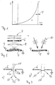
- Figure 2 shows schematically how a converter 5 with an inhomogeneous Light distributions can be applied. This is one way the illumination of a mask 6 with homogeneous light 7 and the subsequent one Image of mask 6 on transducer 5 ( Figure a). In this case the image of the mask 6 is projected onto the converter 5 by means of a lens 8. At the Converter 5 is at a voltage 9. Instead of the single light beam 7 with In a well-defined direction, light rays can come from different Simultaneously hit directions on converter 5.
- two or more coherent waves 10 can be located in the area of the converter 5 be overlaid. Due to the interference, one is formed Intensity pattern ( Figure b).
- Figure 3 shows an embodiment for the practical application of the method.
- a photorefractive material 11 e.g. a photorefractive oxidic Crystal, a photorefractive semiconductor crystal or a photorefractive polymer electrodes 12 can be applied.
- One is connected to one electrode 12a high voltage 6 is applied, the other 12b is connected to earth potential.
- the sample 11 is illuminated with two interfering light beams 13, which are overlay within sample 11.
- Figure 3a Differentiated transmission
- Figure 3b reflection geometry
- the Interference pattern is due to the photorefractive effect in a charge, field and thus refractive index pattern implemented.
Landscapes
- Physics & Mathematics (AREA)
- Nonlinear Science (AREA)
- Chemical & Material Sciences (AREA)
- Engineering & Computer Science (AREA)
- Ceramic Engineering (AREA)
- Crystallography & Structural Chemistry (AREA)
- General Physics & Mathematics (AREA)
- Optics & Photonics (AREA)
- Holo Graphy (AREA)
- Optical Modulation, Optical Deflection, Nonlinear Optics, Optical Demodulation, Optical Logic Elements (AREA)
Abstract
Description
- Figur 1
- die Zunahme der Sensitivität in Abhängigkeit von der Spannung,
- Figur 2
- die Beaufschlagung eines Wandlers mit einem Lichtmuster und
- Figur 3
- ein Anwendungsbeispiel.
Claims (14)
- Verfahren zum Beschreiben eines optischen Modulators mittels elektromagnetischer Schreibstrahlung, wobei der Modulator einen photorefraktiven Wandlerkörper aufweist, in dem die räumlich modulierte Schreibstrahlung Änderungen des Brechungsindex verursacht,
dadurch gekennzeichnet, daß an den Wandlerkörper eine externe Spannung angelegt wird, deren Höhe innerhalb eines Spannungsbereiches gewählt wird, in dem der Aufbau der Brechungsindexänderungen durch eine Erhöhung der Ladungsträgerbeweglichkeit oder Ladungsträgerdichte beschleunigt wird. - Verfahren nach Anspruch 1,
dadurch gekennzeichnet, daß der Wandlerkörper mit Schreibstrahlung inhomogener Intensität beschrieben wird, die ein flächiges oder räumliches Lichtmuster innerhalb des Wandlerkörpers ausbildet, wobei das Lichtmuster ein Brechungsindexmuster erzeugt. - Verfahren nach Anspruch 1 oder 2,
dadurch gekennzeichnet, daß an den Wandlerkörper eine Spannung angelegt wird, deren Höhe dicht unterhalb der Durchschlagspannung des Wandlerkörpers liegt. - Verfahren nach Anspruch 3,
dadurch gekennzeichnet, daßzurErzeugungder Spannung Feldstärken von mehr als 1 kV / cm, insbesondere bis zu 500 kV / cm, angelegt werden. - Verfahren nach einem der vorherigen Ansprüche,
dadurch gekennzeichnet, daß die Inhomogenität der Schreibstrahlung durch eine Maske erzeugt wird, die in den Strahlengang zwischen einer die Schreibstrahlung emittierenden Strahlenquelle und den Wandlerkörper eingebracht wird. - Verfahren nach Anspruch 5,
dadurch gekennzeichnet, daß die Maske die Inhomogenität durch Beugung, Brechung und/oder Reflexion der Schreibstrahlung erzeugt. - Verfahren nach einem der vorherigen Ansprüche,
dadurch gekennzeichnet, daß die Inhomogenität der Schreibstrahlung ein Hologramm in den Wandlerkörper schreibt, das durch Interferenz eines Schreibstrahles mit einem zweiten Strahl innerhalb des Wandlerkörpers erzeugt wird. - Verfahren nach Anspruch 7,
dadurch gekennzeichnet, daß der mit dem Hologramm beschriebene Wandlerkörper mit einem Lesestrahl beleuchtet wird, der durch das Muster insbesondere in seiner Phase, seiner Intensität und/oder seiner Polarisation räumlich moduliert wird. - Verfahren nach Anspruch 8,
dadurch gekennzeichnet, daß die räumliche Modulation des Lesestrahles insbesondere durch ein Interferometer oder einen Polarisator in eine Intensitätsmodulation konvertiert wird. - Verfahren nach Anspruch 7,
dadurch gekennzeichnet, daß das Hologramm mit einem Lesestrahl beleuchtet wird, der sich in seiner Wellenlänge von dem Schreibstrahl unterscheidet, wobei die Bragg-Bedingung erfüllt ist. - Verfahren nach einem der vorherigen Ansprüche,
dadurch gekennzeichnet, daß der Modulator mit zwei miteinander interferierenden Schreibstrahlen beleuchtet wird, die ein Lichtmuster und damit auch ein Brechungsmuster im Wandlerkörper erzeugen und dabei derart an dem Brechungsmuster gebeugt werden, daß einer der Schreibstrahlen auf Kosten des anderen Schreibstrahls verstärkt wird ("optischer Transistor"). - Verfahren nach Anspruch 11,
dadurch gekennzeichnet, daßeinederLichtwelleneine Intensitätsmodulation aufweist und dadurch Bildinformation trägt. - Verfahren nach einem der vorherigen Ansprüche,
dadurch gekennzeichnet, daß der Modulator einen photorefraktiven oxidischen Kristall, einen photorefraktiven Halbleiterkristall oder einen photorefraktives Polymer aufweist. - Vorrichtung zur Durchführung des Verfahrens nach einem der vorherigen Ansprüche.
Applications Claiming Priority (2)
| Application Number | Priority Date | Filing Date | Title |
|---|---|---|---|
| DE10137550A DE10137550A1 (de) | 2001-08-01 | 2001-08-01 | Nichtlineare Steigerung der Photosensitivität bei photorefraktiven Materialien |
| DE10137550 | 2001-08-01 |
Publications (2)
| Publication Number | Publication Date |
|---|---|
| EP1281999A2 true EP1281999A2 (de) | 2003-02-05 |
| EP1281999A3 EP1281999A3 (de) | 2004-09-22 |
Family
ID=34559121
Family Applications (1)
| Application Number | Title | Priority Date | Filing Date |
|---|---|---|---|
| EP02015839A Ceased EP1281999A3 (de) | 2001-08-01 | 2002-07-16 | Nichtlineare Steigerung der Photosensitivität bei photorefraktiven Materialien |
Country Status (4)
| Country | Link |
|---|---|
| US (1) | US6894820B2 (de) |
| EP (1) | EP1281999A3 (de) |
| JP (1) | JP2003121890A (de) |
| DE (1) | DE10137550A1 (de) |
Family Cites Families (9)
| Publication number | Priority date | Publication date | Assignee | Title |
|---|---|---|---|---|
| US4807970A (en) * | 1987-11-23 | 1989-02-28 | International Business Machines Corporation | Holograms in photorefractive materials |
| EP0598761A1 (de) * | 1991-07-26 | 1994-06-01 | Accuwave Corporation | Photorefraktive systeme und methoden |
| US5440669A (en) * | 1991-07-26 | 1995-08-08 | Accuwave Corporation | Photorefractive systems and methods |
| US5508829A (en) * | 1992-12-18 | 1996-04-16 | International Business Machines Corporation | LTG AlGaAs non-linear optical material and devices fabricated therefrom |
| US5422873A (en) * | 1993-03-25 | 1995-06-06 | California Institute Of Technology | Multiplexing and selective updatable fixing and erasing of volume holograms in photorefractive media and second harmonic generation in photorefractive media by optically induced periodic poling |
| US5684612A (en) * | 1993-06-11 | 1997-11-04 | Board Of Trustees Of The Leland Stanford Junior University | Method and system for maintaining and controlling the signal-to-noise ratio of hologams recorded in ferroelectric photorefractive materials |
| US5521743A (en) * | 1993-12-16 | 1996-05-28 | Rockwell International Corporation | Photon-counting spatial light modulator with APD structure |
| JP2001281796A (ja) * | 2000-03-31 | 2001-10-10 | Toshiba Corp | 有機光記録媒体および光記録再生装置 |
| US6549323B1 (en) * | 2001-10-01 | 2003-04-15 | The Boeing Company | Active optical system for phase-shifting desired portions of an incoming optical wavefront |
-
2001
- 2001-08-01 DE DE10137550A patent/DE10137550A1/de not_active Withdrawn
-
2002
- 2002-07-16 EP EP02015839A patent/EP1281999A3/de not_active Ceased
- 2002-07-31 JP JP2002222469A patent/JP2003121890A/ja active Pending
- 2002-08-01 US US10/211,768 patent/US6894820B2/en not_active Expired - Fee Related
Non-Patent Citations (1)
| Title |
|---|
| DAUTET H. ET AL: "Photon counting techniques with silicon avalanche photodiodes", APPLIED OPTICS, vol. 32, no. 21, 20 July 1993 (1993-07-20), pages 3894 - 3900, XP000382656 * |
Also Published As
| Publication number | Publication date |
|---|---|
| US6894820B2 (en) | 2005-05-17 |
| US20040021925A1 (en) | 2004-02-05 |
| JP2003121890A (ja) | 2003-04-23 |
| DE10137550A1 (de) | 2003-03-27 |
| EP1281999A3 (de) | 2004-09-22 |
Similar Documents
| Publication | Publication Date | Title |
|---|---|---|
| DE3786377T2 (de) | Optische Dünnschicht-Bauteile. | |
| DE69103310T2 (de) | Räumlicher Lichtmodulator mit Flüssigkristall und Gerät zur holographischen Aufzeichnung von Bildinformationen, das diesen benutzt. | |
| EP0021754B1 (de) | Elektrooptischer Modulator und seine Verwendung | |
| DE4092522C2 (de) | Vorrichtung zur rein optischen Bildverarbeitung und Mustererkennung unter Verwendung stimulierter Photonechos | |
| DE2812956C2 (de) | ||
| DE2218309A1 (de) | Optische Steuereinrichtung | |
| DE112008002830T5 (de) | Optische Maske und Lichtquellengerät | |
| DE69905622T2 (de) | Optische vorrichtung | |
| DE68908132T2 (de) | Optisches lichtventilsystem zur erzeugung eines phasenkonjugierten strahls steuerbarer intensität. | |
| DE69017643T2 (de) | Optische Verarbeitung mit einer mehrschichtigen Heterostruktur. | |
| DE60209561T2 (de) | Aktives optisches system zur phasenverschiebung gewünschter bereiche einer eintreffenden optischen wellenfront | |
| DE69023820T2 (de) | Holographisches optisches Gerät. | |
| DE69227221T2 (de) | Räumlicher Lichtmodulator mit Flüssigkristall | |
| DE2032108A1 (de) | Volumenholographische Vorrichtung | |
| DE2246030C2 (de) | Holographisches System zur Bildung eines Brechungsindexgitters im Innern einer durch Licht erregbaren ferroelektrischen Kristallplatte | |
| DE2256515A1 (de) | Holographisches system zur bildung eines indexnetzes im volumen eines polykristallinen plaettchens aus einem lichtempfindlichen, elektronenoptischen werkstoff | |
| DE2320521A1 (de) | Optisches beugungssystem | |
| DE2345351C2 (de) | Holographisches Aufzeichnungs- und Auslesesystem | |
| DE3929817A1 (de) | Geraet der informationstechnik unter verwendung von laserlicht | |
| DE60130706T2 (de) | Optische Abtastvorrichtung und optisches Informationsaufzeichnungs- /-wiedergabegerät | |
| DE1283963B (de) | Verfahren zur steuerbaren Richtungsablenkung optischer Strahlung, insbesondere von Laser-Strahlung, und Vorrichtung zur Durchfuehrung desselben | |
| DE2120006C3 (de) | Holographischer Speicher | |
| DE2515373A1 (de) | Holographische speichervorrichtung | |
| DE10137550A1 (de) | Nichtlineare Steigerung der Photosensitivität bei photorefraktiven Materialien | |
| DE69020697T2 (de) | Frequenzverdoppelnder optischer Wellenleiter mit aktiver Phasenanpassung und Frequenzverdoppelungssystem. |
Legal Events
| Date | Code | Title | Description |
|---|---|---|---|
| PUAI | Public reference made under article 153(3) epc to a published international application that has entered the european phase |
Free format text: ORIGINAL CODE: 0009012 |
|
| AK | Designated contracting states |
Designated state(s): AT BE BG CH CY CZ DE DK EE ES FI FR GB GR IE IT LI LU MC NL PT SE SK TR |
|
| AX | Request for extension of the european patent |
Extension state: AL LT LV MK RO SI |
|
| PUAL | Search report despatched |
Free format text: ORIGINAL CODE: 0009013 |
|
| AK | Designated contracting states |
Kind code of ref document: A3 Designated state(s): AT BE BG CH CY CZ DE DK EE ES FI FR GB GR IE IT LI LU MC NL PT SE SK TR |
|
| AX | Request for extension of the european patent |
Extension state: AL LT LV MK RO SI |
|
| 17P | Request for examination filed |
Effective date: 20050322 |
|
| AKX | Designation fees paid |
Designated state(s): AT BE BG CH CY CZ DE DK EE ES FI FR GB GR IE IT LI LU MC NL PT SE SK TR |
|
| 17Q | First examination report despatched |
Effective date: 20050517 |
|
| 17Q | First examination report despatched |
Effective date: 20050517 |
|
| STAA | Information on the status of an ep patent application or granted ep patent |
Free format text: STATUS: THE APPLICATION HAS BEEN REFUSED |
|
| 18R | Application refused |
Effective date: 20090213 |