EP1280384A2 - Dimm-Modul - Google Patents
Dimm-Modul Download PDFInfo
- Publication number
- EP1280384A2 EP1280384A2 EP02011283A EP02011283A EP1280384A2 EP 1280384 A2 EP1280384 A2 EP 1280384A2 EP 02011283 A EP02011283 A EP 02011283A EP 02011283 A EP02011283 A EP 02011283A EP 1280384 A2 EP1280384 A2 EP 1280384A2
- Authority
- EP
- European Patent Office
- Prior art keywords
- dimming
- dimming module
- load
- control signal
- source
- Prior art date
- Legal status (The legal status is an assumption and is not a legal conclusion. Google has not performed a legal analysis and makes no representation as to the accuracy of the status listed.)
- Granted
Links
Images

Classifications
-
- H—ELECTRICITY
- H05—ELECTRIC TECHNIQUES NOT OTHERWISE PROVIDED FOR
- H05B—ELECTRIC HEATING; ELECTRIC LIGHT SOURCES NOT OTHERWISE PROVIDED FOR; CIRCUIT ARRANGEMENTS FOR ELECTRIC LIGHT SOURCES, IN GENERAL
- H05B39/00—Circuit arrangements or apparatus for operating incandescent light sources
- H05B39/04—Controlling
- H05B39/041—Controlling the light-intensity of the source
- H05B39/044—Controlling the light-intensity of the source continuously
- H05B39/047—Controlling the light-intensity of the source continuously with pulse width modulation from a DC power source
-
- Y—GENERAL TAGGING OF NEW TECHNOLOGICAL DEVELOPMENTS; GENERAL TAGGING OF CROSS-SECTIONAL TECHNOLOGIES SPANNING OVER SEVERAL SECTIONS OF THE IPC; TECHNICAL SUBJECTS COVERED BY FORMER USPC CROSS-REFERENCE ART COLLECTIONS [XRACs] AND DIGESTS
- Y02—TECHNOLOGIES OR APPLICATIONS FOR MITIGATION OR ADAPTATION AGAINST CLIMATE CHANGE
- Y02B—CLIMATE CHANGE MITIGATION TECHNOLOGIES RELATED TO BUILDINGS, e.g. HOUSING, HOUSE APPLIANCES OR RELATED END-USER APPLICATIONS
- Y02B20/00—Energy efficient lighting technologies, e.g. halogen lamps or gas discharge lamps
Definitions
- the invention is based on a dimming module according to the preamble of claim 1. It is in particular a dimming module that provides a variable additional load for a direct current or direct voltage source.
- a direct current or direct voltage source is not only to be understood as ideal sources, but also sources that have a finite source resistance.
- electrical consumers are to be understood, such as. B. are incandescent lamps or light emitting diodes. Dimming is understood to mean the power delivered to the load, based on the maximum power that can be output. The dimming setting is usually expressed in%.
- the dimming module contains a resistor that permanently provides power sourced from the direct current or direct voltage source.
- the term resistance is to be understood broadly in this context: The desired effect can be achieved by any electrical component that has an impedance with a real part. The value of the resistance is dimensioned such that the DC or DC voltage source operates stably even in the event that the load no longer consumes power.
- the power absorbed by the resistor is chosen to be indirectly proportional to the dimming position. This can apply to an entire dimming range from 0% to 100%. With a dimming setting of 0%, the resistance takes up the minimum power required for stable operation of the direct current or direct voltage source. When the dimming position is increased, the power consumed by the resistor is reduced. At 100% dimming, the resistor does not take up any power.
- the linear relationship between dimming and resistance consumed power can also be limited to a range for the dimmer setting. In this case, below a given dimming position, the resistance constantly consumes the minimum power that is required for stable operation of the direct current or direct voltage source. Above a given further dimming position, the power consumed by the resistor is constantly zero.
- the load is preferably operated in pulsed mode.
- the power consumed by the load there is an on-state in which the maximum power that can be delivered to the load by the direct current or voltage source is delivered to the load and an off-state in which the power delivered to the load is zero .
- the ratio of the length of the time intervals in which a state is assumed determines the average power that is delivered to the load.
- power is delivered to the resistor only in the off state. According to the invention, if more average power is delivered to the load, the time in which power is delivered to the resistor is shortened, and thus also the average power that is delivered to the resistor. Because the DC or DC source supplies power to either the load or the resistor, the source never has to provide the sum of both powers.
- the direct current or direct voltage source can thus be designed to be weaker and uses less power loss.
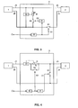
- the dimming module 3 has two source connections J1 and J2 at which a direct current or direct voltage source 1 feeds power into the dimming module.
- the dimming module 3 has two load connections J3 and J4 to which a load 2 is connected. Connections J1 and J3 are connected in dimming module 3.
- the pulsed operation of the load is realized in that the connections J2 and J4 are connected to one another via a switch S 1.
- the switch S1 is thus in series with a load connection.
- the switch S 1 is controlled by a control signal A1.
- the course of the control signal A1 over time t is shown as an example.
- control signal A1 assumes the value H1
- the switch S1 is closed and the dimming module is in the on state. If the control signal assumes the value 0, the switch S 1 is open and the dimming module is in the off state. In the example in FIG. 2, a dimming setting of approx. 66% is set.
- the series circuit comprising a resistor R and a switch S2 is connected in parallel with the source connections J1 and J2 in FIG. 1.
- the switch S2 is controlled by a control signal A2.
- this profile is inverse to the profile of the control signal A1. Whenever switch S1 is closed and power is delivered to the load, switch S2 is open and resistor R does not take up any power. In the opposite case, switch S 1 is open and switch S2 is closed. Then only power is delivered to the resistor R.
- control signal A1 not only controls the switch S1, but it is also fed into an inverter 31.
- the inverter 31 outputs the control signal A1 inverted at its output as the control signal A2 to the switch S2.
- the control signal A1 is generated by an evaluation device 32.
- the evaluation device 32 has a control input C, with the aid of which the information about the desired dimming position is fed to the dimming module 3.
- the evaluation device 32 evaluates this information and generates a control signal A1 which realizes the desired dimming position.
- a pulse width modulator is preferably used for the evaluation device 32.
- the control input C does not necessarily have to obtain its information from outside the dimming module 3. It is also possible that, for example, a potentiometer setting or a position of a selector switch within the dimming module 3 defines the dimming position.
- FIG. 3 shows a block diagram of a further exemplary embodiment of a dimming module according to the invention. It essentially corresponds to the exemplary embodiment in FIG. 1. The same or equivalent elements have the same designation in both figures.
- a voltage measuring device 33 is added in FIG. 3. It is connected in parallel to the source connections J1 and J2. Their purpose is described in the following: If the dimming module 3 is intended for operation on different direct current or direct voltage sources 1, it may be necessary for the value of the resistance R to be dependent on the source voltage which is present at the source connections J1 and J2, is made.
- the voltage measuring device 33 evaluates the source voltage and sets the value provided for the resistor R. The evaluation of the source voltage can be done in different ways. B.
- an average value of the source voltage is formed and this is then compared with a predetermined threshold. This is advantageous if the value of the source voltage is subject to strong fluctuations.
- the evaluation of the source voltage can also be time-dependent: for example, the evaluation can only take place in periods in which the switch S2 is closed; this variant should be chosen if the setting of the value of the resistance R should be independent of the load.
- the setting itself can be done with the help of a relay that connects different resistors.
- the resistor R is designed as an electronically controllable resistor (eg MOSFET) which is controlled by the voltage measuring device 33.
- the information about which value is required for the resistor R so that the direct voltage or direct current source works stably in the lowest dimming position can also be supplied to the dimming module by the direct voltage or direct current source in a separate way. In this case there is no need to evaluate the source voltage. However, additional effort for the above Transmission of information necessary. This can be done in the form of an additional electrical line from the DC voltage or DC source to the dimming module. If an additional line is not desired e.g. B. a coding plug can be used, which makes the requirements of the DC voltage or DC source with respect to the value of the resistance R accessible to the dimming module. The advantage of a coding plug can be seen in the fact that no intervention is necessary in the direct voltage or direct current source itself, and any direct voltage or direct current source can thus be selected.
- FIG. 4 shows a block diagram of a further exemplary embodiment of a dimming module according to the invention.
- a dual circuit is shown in FIG. 4.
- the same or equivalent elements have the same designation in both figures.
- the comments on the mode of operation and design of the elements from FIGS. 1 and 3 can be transferred to FIG. 4.
- the exemplary embodiments in FIGS. 1 and 3 are preferably to be used for sources 1 which have the character of a voltage source. This applies in cases in which the source resistance of a source 1 is less than the effective resistance of a load 2.
- an embodiment according to FIG. 4 is to be selected if a source 1 has the character of a current source. This is the case if the source resistance of source 1 is greater than the effective resistance of a load 2.
- the switch S1 is connected in parallel to the load connections J3 and J4. In contrast to the exemplary embodiments in FIGS. 1 and 3, power is therefore only fed into load 2 when switch S1 is open.
- the resistor R is connected in series to a source connection J1 in FIG. 4 and the switch S2 is connected in parallel. Power is then fed into the resistor R when the switch S2 is open.
- An evaluation device 32 supplies the same signal as in the exemplary embodiments in FIGS. 1 and 3. Since the switches S1 and S2 now have the opposite effect in comparison to the exemplary embodiments in FIGS. 1 and 3, the evaluation device 32 controls in FIG 4 directly the switch S2, while the switch S1 is controlled by an inverter 31.
- a current measuring device 33 is connected in series with the resistor R. It sets the value of resistance R to match source 1.
- suitable means that the value of the resistor R is selected so that the source 1 works stably in the lowest dimming position. If the dimming module 3 is only intended for one type of source 1, the current measuring device 33 can be omitted.
Landscapes
- Circuit Arrangement For Electric Light Sources In General (AREA)
Abstract
Description
- Die Erfindung geht aus von einem Dimm-Modul gemäß dem Oberbegriff des Anspruchs 1. Es handelt sich dabei insbesondere um ein Dimm-Modul, das für eine Gleichstrom- oder Gleichspannungsquelle eine variable Zusatzlast bereit stellt.
- Oft besteht der Wunsch, dass die Leistung, die eine Gleichstrom- oder Gleichspannungsquelle an eine Last abgibt, abhängig von einer gewünschten Dimmstellung einstellbar ist. Dazu wird die Last nicht direkt an die Gleichstrom- oder Gleichspannungsquelle angeschlossen, sondern es wird ein Dimm-Modul zwischen die Gleichstrom- oder Gleichspannungsquelle und die Last geschaltet. Unter Gleichstrom- oder Gleichspannungsquelle sind nicht ausschließlich ideale Quellen zu verstehen, sondern auch Quellen, die einen endlichen Quellwiderstand aufweisen. Unter Last sind elektrische Verbraucher zu verstehen, wie es z. B. Glühlampen oder Leuchtdioden sind. Unter Dimmstellung wird die an die Last abgegebene Leistung, bezogen auf die maximal abgebbare Leistung verstanden. Meist wird die Dimmstellung in % ausgedrückt.
- Ein Problem entsteht dadurch, dass viele Gleichstrom- oder Gleichspannungsquellen, insbesondere solche, die getaktete Wandler enthalten, eine Minimallast erfordern. Bei niedriger Dimmstellung arbeitet die Gleichstrom- oder Gleichspannungsquelle nicht mehr stabil. Entsprechend dem Stand der Technik wird dieses Problem dadurch gelöst, dass das Dimm-Modul einen Widerstand enthält, der permanent eine Leistung von der Gleichstrom- oder Gleichspannungsquelle bezieht. Der Begriff Widerstand ist in diesem Zusammenhang weit zu fassen: Die gewünschte Wirkung kann jedes elektrische Bauelement erfüllen, das eine Impedanz mit einem Realteil aufweist. Der Wert des Widerstandes ist so bemessen, dass auch für den Fall, dass die Last keine Leistung mehr aufnimmt, die Gleichstrom- oder Gleichspannungsquelle stabil arbeitet. Nachteil dieser Lösung ist, dass auch bei einer hohen Dimmstellung, bei der der Widerstand zur Stabilisierung nicht mehr nötig ist, der Widerstand Leistung aufnimmt. Dadurch wird unnötig Leistung verbraucht. Dies nicht nur im Widerstand, sondern auch in der Gleichstrom- oder Gleichspannungsquelle, die bedingt durch den Widerstand eine höhere Ausgangsleistung liefern muss. Zudem muss die Gleichstrom- oder Gleichspannungsquelle für eine Leistung ausgelegt sein, die der Summe der Leistungen entspricht, die von der Last und vom Widerstand aufgenommen werden.
- Es ist Aufgabe der vorliegenden Erfindung, ein Dimm-Modul gemäß dem Oberbegriff des Anspruchs 1 bereitzustellen, das einen Widerstand enthält, der nur bei niedriger Dimmstellung die zur Stabilisierung der Gleichstrom- oder Gleichspannungsquelle nötige Leistung aufnimmt.
- Diese Aufgabe wird durch ein Dimm-Modul mit den Merkmalen des Oberbegriffs des Anspruchs 1 durch die Merkmale des kennzeichnenden Teils des Anspruchs 1 gelöst. Besonders vorteilhafte Ausgestaltungen finden sich in den abhängigen Ansprüchen.
- Erfindungsgemäß wird die Leistung, die der Widerstand aufnimmt, indirekt proportional zur Dimmstellung gewählt. Dies kann für einen gesamten Dimmbereich von 0% bis 100% gelten. Bei einer Dimmstellung von 0% nimmt der Widerstand die Minimalleistung auf, für einen stabilen Betrieb der Gleichstrom- oder Gleichspannungsquelle nötig ist. Bei Erhöhung der Dimmstellung wird die vom Widerstand aufgenommene Leistung reduziert. Bei 100% Dimmstellung nimmt der Widerstand keine Leistung auf. Der lineare Zusammenhang zwischen Dimmstellung und der vom Widerstand aufgenommenen Leistung kann auch auf einen Bereich für die Dimmstellung eingeschränkt sein. Unterhalb einer gegebenen Dimmstellung nimmt in diesem Fall der Widerstand konstant die Minimalleistung auf, die für einen stabilen Betrieb der Gleichstrom- oder Gleichspannungsquelle nötig ist. Oberhalb einer gegebenen weiteren Dimmstellung ist die vom Widerstand aufgenommene Leistung konstant Null.
- Zur Einstellung der von der Last aufgenommenen Leistung wird die Last bevorzugt gepulst betreiben. Für die von der Last aufgenommene Leistung gibt es einen Ein-Zustand, in dem die maximal von der Gleichstrom- oder Gleichspannungsquelle an die Last abgebbare Leistung an die Last abgegeben wird und einen Aus-Zustand, in dem die an die Last abgegebene Leistung Null ist. Das Verhältnis der Länge der Zeitintervalle in denen jeweils ein Zustand angenommen wird, bestimmt die mittlere Leistung, die an die Last abgegeben wird. Erfindungsgemäß wird an den Widerstand nur im Aus-Zustand Leistung abgegeben. Wird mehr mittlere Leistung an die Last abgegeben, verkürzt sich erfindungsgemäß die Zeit, in der Leistung an den Widerstand abgegeben wird und damit auch die mittlere Leistung, die an den Widerstand abgegeben wird. Da die Gleichstrom- oder Gleichspannungsquelle entweder an die Last oder an den Widerstand Leistung abgibt, muss die Quelle nie die Summe beider Leistungen liefern. Die Gleichstrom- oder Gleichspannungsquelle kann somit schwächer ausgelegt werden und verbraucht weniger Verlustleistung.
- Im folgenden soll die Erfindung anhand von Ausführungsbeispielen näher erläutert werden. Es zeigen:
- Figur 1
- ein Blockschaltbild eines Ausführungsbeispiels eines erfindungsgemäßen Dimm-Moduls,
- Figur 2
- den zeitlichen Verlauf von erfindungsgemäßen Steuersignalen,
- Figur 3
- ein Blockschaltbild eines weiteren Ausführungsbeispiels eines erfindungsgemäßen Dimm-Moduls,
- Figur 4
- ein Blockschaltbild eines zu Fig. 3 dualen Ausführungsbeispiels eines erfindungsgemäßen Dimm-Moduls
- In Fig. 1 ist ein Blockschaltbild eines Ausführungsbeispiels eines erfindungsgemäßen Dimm-Moduls dargestellt. Das Dimm-Modul 3 besitzt zwei Quellanschlüsse J1 und J2 an denen eine Gleichstrom- oder Gleichspannungsquelle 1 Leistung in das Dimm-Modul einspeist. Das Dimm-Modul 3 besitzt zwei Lastanschlüsse J3 und J4 an denen eine Last 2 angeschlossen ist. Im Dimm-Modul 3 sind die Anschlüsse J1 und J3 verbunden. Der gepulste Betrieb der Last wird dadurch realisiert, dass die Anschlüsse J2 und J4 über einen Schalter S 1 miteinander verbunden sind. Der Schalter S1 liegt somit in Serie zu einem Lastanschluss. Der Schalter S 1 wird von einem Steuersignal A1 gesteuert. Im oberen Abschnitt von Fig.2 ist beispielhaft der Verlauf des Steuersignals A1 über der Zeit t dargestellt. Nimmt das Steuersignal A1 den Wert H1 an, ist der Schalter S1 geschlossen und das Dimm-Modul befindet sich im Ein-Zustand. Nimmt das Steuersignal den Wert 0 an ist der Schalter S 1 offen und das Dimm-Modul befindet sich im Aus-Zustand. Im Beispiel in Fig. 2 ist eine Dimmstellung von ca. 66% eingestellt.
- Parallel zu den Quellanschlüssen J1 und J2 in Fig. 1 ist die Serienschaltung aus einem Widerstand R und einem Schalter S2 geschaltet. Der Schalter S2 wird von einem Steuersignal A2 gesteuert. Im unteren Abschnitt von Fig.2 ist beispielhaft der Verlauf des Steuersignals A2 über der Zeit t dargestellt. Erfindungsgemäß ist dieser Verlauf invers zum Verlauf des Steuersignals A1. Immer wenn der Schalter S1 geschlossen ist und Leistung an die Last abgegeben wird, ist der Schalter S2 geöffnet und der Widerstand R nimmt keine Leistung auf. Im umgekehrten Fall ist der Schalter S 1 geöffnet und der Schalter S2 geschlossen. Dann wird nur Leistung an den Widerstand R abgegeben.
- Gemäß Fig. 1 steuert das Steuersignal A1 nicht nur den Schalter S1, vielmehr wird es zusätzlich in einen Inverter 31 eingespeist. Der Inverter 31 gibt das Steuersignal A1 an seinem Ausgang invertiert als Steuersignal A2 an den Schalter S2 aus.
- Erzeugt wird das Steuersignal A1 von einer Auswerteeinrichtung 32. Die Auswerteeinrichtung 32 besitzt einen Kontrolleingang C, mit dessen Hilfe die Information über die gewünschte Dimmstellung dem Dimm-Modul 3 zugeführt wird. Die Auswerteeinrichtung 32 wertet diese Information aus und erzeugt ein Steuersignal A1, das die gewünschte Dimmstellung realisiert. Bevorzugt wird für die Auswerteeinrichtung 32 ein Pulsweitenmodulator eingesetzt.
- Der Kontrolleingang C muss nicht zwangsläufig seine Information von außerhalb des Dimm-Moduls 3 beziehen. Es ist auch möglich, dass beispielsweise eine Potentiometereinstellung oder eine Stellung eines Wahlschalters innerhalb des Dimm-Moduls 3 die Dimmstellung festlegt.
- In Fig. 3 ist ein Blockschaltbild eines weiteren Ausführungsbeispiels eines erfindungsgemäßen Dimm-Moduls dargestellt. Im wesentlichen entspricht es dem Ausführungsbeispiel in Fig.1. Gleiche bzw. gleich wirkende Elemente tragen in beiden Figuren die gleiche Bezeichnung. Bezüglich Fig. 1 ist in Fig. 3 eine Spannungsmesseinrichtung 33 hinzugefügt. Sie ist parallel zu den Quellanschlüssen J1 und J2 geschaltet. Ihr Zweck wird im folgenden beschrieben: Ist das Dimm-Modul 3 zum Betrieb an unterschiedlichen Gleichstrom- oder Gleichspannungsquellen 1 vorgesehen, so kann es nötig sein, dass der Wert des Widerstands R abhängig von der Quellspannung, die an den Quellanschlüssen J1 und J2 anliegt, gemacht wird. Die Spannungsmesseinrichtung 33 wertet die Quellspannung aus und stellt den dazu vorgesehenen Wert für den Widerstand R ein. Die Auswertung der Quellspannung kann auf unterschiedliche Weise geschehen: Es kann z. B. erst ein Mittelwert der Quellspannung gebildet werden und dieser dann mit einer vorgegebenen Schwelle verglichen werden. Dies ist vorteilhaft, wenn der Wert der Quellspannung starken Schwankungen unterliegt. Die Auswertung der Quellspannung kann auch zeitabhängig sein: Z. B. kann die Auswertung nur in Zeitabschnitten erfolgen, in denen der Schalter S2 geschlossen ist; diese Variante ist zu wählen, falls die Einstellung des Werts des Widerstandes R unabhängig von der Last sein soll. Die Einstellung selbst kann mit Hilfe eines Relais geschehen, das unterschiedliche Widerstände zuschaltet. Es ist aber auch denkbar, dass der Widerstand R als elektronisch steuerbarer Widerstand (z.B. MOSFET) ausgeführt ist, der von der Spannungsmesseinrichtung 33 gesteuert wird.
- Die Information darüber, welcher Wert für den Widerstand R erforderlich ist, damit die Gleichspannungs- oder Gleichstromquelle in der niedrigsten Dimmstellung stabil arbeitet, kann von der Gleichspannungs- oder Gleichstromquelle dem Dimm-Modul auch auf separatem Wege zugeführt werden. In diesem Fall kann auf die Auswertung der Quellspannung verzichtet werden. Allerdings ist zusätzlicher Aufwand für die o.g. Informationsübermittlung nötig. Dies kann in Form einer zusätzlichen elektrischen Leitung von der Gleichspannungs- oder Gleichstromquelle zum Dimm-Modul geschehen. Falls eine zusätzliche Leitung nicht gewünscht wird kann z. B. ein Kodierstecker verwendet werden, der die Erfordernisse der Gleichspannungs- oder Gleichstromquelle bezüglich des Werts des Widerstandes R dem Dimm-Modul zugänglich macht. Der Vorteil eines Kodiersteckers ist darin zu sehen, dass in der Gleichspannungs- oder Gleichstromquelle selbst kein Eingriff nötig ist und damit eine beliebige Gleichspannungs- oder Gleichstromquelle gewählt werden kann.
- In Fig. 4 ist ein Blockschaltbild eines weiteren Ausführungsbeispiels eines erfindungsgemäßen Dimm-Moduls dargestellt. Bezüglich den Ausführungsbeispielen in Fig. 1 und 3 ist in Fig. 4 eine dazu duale Schaltung dargestellt. Gleiche bzw. gleich wirkende Elemente tragen in beiden Figuren die gleiche Bezeichnung. Die Bemerkungen zur Wirkungsweise und Ausführung der Elemente aus Fig. 1 und 3 können auf Fig. 4 übertragen werden. Die Ausführungsbeispiele in den Fig. 1 und 3 sind bevorzugt bei Quellen 1 zu verwenden, die den Charakter eine Spannungsquelle haben. Das gilt in den Fällen, in denen der Quellwiderstand einer Quelle 1 kleiner ist als der wirksame Widerstand einer Last 2. Umgekehrt ist eine Ausführung gemäß Fig. 4 zu wählen falls eine Quelle 1 den Charakter einer Stromquelle hat. Dies ist dann der Fall, wenn der Quellwiderstand der Quelle 1 größer ist als der wirksame Widerstand einer Last 2.
- Der Schalter S1 ist in Fig. 4 parallel zu den Lastanschlüssen J3 und J4 geschaltet. Damit wird im Gegensatz zu den Ausführungsbeispielen in Fig. 1 und 3 nur Leistung in die Last 2 eingespeist, wenn der Schalter S1 geöffnet ist. Der Widerstand R ist in Fig. 4 seriell zu einem Quellanschluss J1 geschaltet und der Schalter S2 parallel dazu geschaltet. In den Widerstand R wird dann Leistung eingespeist, wenn der Schalter S2 geöffnet ist. Eine Auswerteeinrichtung 32 liefert das gleiche Signal wie in den Ausführungsbeispielen in Fig. 1 und Fig. 3. Da die Schalter S1 und S2 im Vergleich zu den Ausführungsbeispielen in Fig. 1 und Fig. 3 nun umgekehrte Wirkung haben, steuert die Auswerteeinrichtung 32 in Fig. 4 direkt den Schalter S2, während der Schalter S1 über einen Inverter 31 gesteuert wird.
- Eine Strommesseinrichtung 33 ist seriell zum Widerstand R geschaltet. Sie stellt den Wert des Widerstandes R passend zur Quelle 1 ein. Passend bedeutet in diesem Zusammenhang, dass der Wert des Widerstandes R so gewählt wird, dass die Quelle 1 in der niedrigsten Dimmstellung stabil arbeitet. Ist das Dimm-Modul 3 nur für einen Typ von Quellen 1 vorgesehen, kann die Strommesseinrichtung 33 entfallen.
Claims (12)
- Dimm-Modul (3), mit Quell- und Lastanschlüssen (J1, J2, J3, J4), das zwischen eine Gleichstrom- oder Gleichspannungsquelle (1) und eine Last (2) geschaltet ist und das eine Einstellung der mittleren, von der Last (2) aufgenommenen Leistung ermöglicht,
dadurch gekennzeichnet, dass das Dimm-Modul (3) einen Widerstand (R) enthält, der innerhalb eines Dimmbereichs eine mittlere Leistung aufnimmt, die indirekt proportional zur von der Last (2) aufgenommenen mittleren Leistung ist. - Dimm-Modul (3) gemäß Anspruch 1, dadurch gekennzeichnet, dass sich der Dimmbereich von einer Dimmstellung 0% bis zu einer Dimmstellung 100% erstreckt.
- Dimm-Modul (3) gemäß Anspruch 1 oder 2, gekennzeichnet durch folgende Merkmale:• die von der Last (2) aufgenommene Leistung ist gepulst,• der Widerstand (R) nimmt nur in Zeitintervallen Leistung auf, in denen die Last (2) keine Leistung aufnimmt.
- Dimm-Modul (3) gemäß Anspruch 1 oder 2, gekennzeichnet durch folgende Merkmale:• seriell zu einem Lastanschluss (J3, J4) ist ein erster Schalter (S1) geschaltet, der von einem ersten Steuersignal (A1) gesteuert wird,• seriell zum Widerstand (R) ist ein zweiter Schalter (S2) geschaltet, der von einem zweiten Steuersignal (A2) gesteuert wird,• erstes und zweites Steuersignal (Al, A2) sind invers zueinander.
- Dimm-Modul (3) gemäß Anspruch 4, dadurch gekennzeichnet, dass das Dimm-Modul (3) einen Inverter (31) enthält, der das zweite Steuersignal (A2) aus dem ersten (A1) generiert.
- Dimm-Modul (3) gemäß Anspruch 1 oder 2, gekennzeichnet durch folgende Merkmale:• parallel zu den Lastanschlüssen (J3, J4) ist ein erster Schalter (S1) geschaltet, der von einem ersten Steuersignal (A1) gesteuert wird,• parallel zum Widerstand (R) ist ein zweiter Schalter (S2) geschaltet, der von einem zweiten Steuersignal (A2) gesteuert wird,• erstes und zweites Steuersignal (A1, A2) sind invers zueinander.
- Dimm-Modul (3) gemäß Anspruch 6, dadurch gekennzeichnet, dass das Dimm-Modul (3) einen Inverter (31) enthält, der das erste Steuersignal (A1) aus dem zweiten (A2) generiert.
- Dimm-Modul (3) gemäß Anspruch 5, dadurch gekennzeichnet, dass das Dimm-Modul (3) einen Kontroll-Eingang (C) und eine Auswerteeinrichtung (32) besitzt, wobei dem Kontroll-Eingang (C) ein Signal zugeführt wird, das eine Information über die gewünschte Dimmstellung enthält und die Auswerteeinrichtung (32) diese Information benützt, um das erste Steuersignal (A1) zu erzeugen.
- Dimm-Modul(3) gemäß Anspruch 7, dadurch gekennzeichnet, dass das Dimm-Modul (3) einen Kontroll-Eingang (C) und eine Auswerteeinrichtung (32) besitzt, wobei dem Kontroll-Eingang (C) ein Signal zugeführt wird, das eine Information über die gewünschte Dimmstellung enthält und die Auswerteeinrichtung (32) diese Information benützt, um das zweite Steuersignal (A2) zu erzeugen.
- Dimm-Modul (3) gemäß Anspruch 1 oder 2, dadurch gekennzeichnet, dass es sich bei der Last (2) um eine Leuchtdiode handelt.
- Dimm-Modul (3) gemäß Anspruch 1 oder 2, dadurch gekennzeichnet, dass das Dimm-Modul (3) eine Spannungs- oder Strommess-Einrichtung (33) enthält, die eine Veränderung des Werts des Widerstandes (R) abhängig vom Wert der oder des von der Gleichspannungs- oder Gleichstromquelle (1) gelieferten Spannung oder Stroms bewirkt.
- Dimm-Modul (3) gemäß Anspruch 1 oder 2, dadurch gekennzeichnet, dass die Information über den Wert des Widerstands (R), von der Gleichspannungs- oder Gleichstromquelle (1) dem Dimm-Modul (3) auf separatem Wege zugeführt wird.
Applications Claiming Priority (2)
| Application Number | Priority Date | Filing Date | Title |
|---|---|---|---|
| DE10136658 | 2001-07-27 | ||
| DE10136658A DE10136658A1 (de) | 2001-07-27 | 2001-07-27 | Dimm-Modul |
Publications (3)
| Publication Number | Publication Date |
|---|---|
| EP1280384A2 true EP1280384A2 (de) | 2003-01-29 |
| EP1280384A3 EP1280384A3 (de) | 2005-01-12 |
| EP1280384B1 EP1280384B1 (de) | 2008-07-16 |
Family
ID=7693321
Family Applications (1)
| Application Number | Title | Priority Date | Filing Date |
|---|---|---|---|
| EP02011283A Expired - Lifetime EP1280384B1 (de) | 2001-07-27 | 2002-05-22 | Dimm-Modul |
Country Status (3)
| Country | Link |
|---|---|
| EP (1) | EP1280384B1 (de) |
| AT (1) | ATE401762T1 (de) |
| DE (2) | DE10136658A1 (de) |
Cited By (1)
| Publication number | Priority date | Publication date | Assignee | Title |
|---|---|---|---|---|
| US7385495B2 (en) | 2004-10-18 | 2008-06-10 | Volkswagen Ag | Illumination device for vehicles and method for controlling an illumination device for vehicles |
Families Citing this family (1)
| Publication number | Priority date | Publication date | Assignee | Title |
|---|---|---|---|---|
| DE102007044339B4 (de) * | 2007-09-17 | 2020-08-20 | Tridonic Gmbh & Co Kg | Leuchtdioden-Modul und Verfahren zur Steuerung eines Leuchtdioden-Moduls |
Citations (6)
| Publication number | Priority date | Publication date | Assignee | Title |
|---|---|---|---|---|
| US4668906A (en) * | 1985-07-11 | 1987-05-26 | Ekstrand John P | Switched resistor regulator |
| US4719404A (en) * | 1985-07-11 | 1988-01-12 | Spectra-Physics, Inc. | Switched resistor regulator with linear dissipative regulator |
| EP0716485A1 (de) * | 1994-12-05 | 1996-06-12 | Hughes Aircraft Company | Stromquelle für Dioden-Ansteuerung |
| US5631523A (en) * | 1995-09-19 | 1997-05-20 | Beacon Light Products, Inc. | Method of regulating lamp current through a fluorescent lamp by pulse energizing a driving supply |
| US5811940A (en) * | 1994-06-22 | 1998-09-22 | Physiomed-Medizintechnik Gmbh | Phase-shift lamp control |
| DE19943256A1 (de) * | 1999-09-10 | 2001-03-15 | Hella Kg Hueck & Co | Vorrichtung und Verfahren zur Ansteuerung einer Lichteinheit für Fahrzeuge |
-
2001
- 2001-07-27 DE DE10136658A patent/DE10136658A1/de not_active Withdrawn
-
2002
- 2002-05-22 AT AT02011283T patent/ATE401762T1/de not_active IP Right Cessation
- 2002-05-22 EP EP02011283A patent/EP1280384B1/de not_active Expired - Lifetime
- 2002-05-22 DE DE50212496T patent/DE50212496D1/de not_active Expired - Lifetime
Patent Citations (6)
| Publication number | Priority date | Publication date | Assignee | Title |
|---|---|---|---|---|
| US4668906A (en) * | 1985-07-11 | 1987-05-26 | Ekstrand John P | Switched resistor regulator |
| US4719404A (en) * | 1985-07-11 | 1988-01-12 | Spectra-Physics, Inc. | Switched resistor regulator with linear dissipative regulator |
| US5811940A (en) * | 1994-06-22 | 1998-09-22 | Physiomed-Medizintechnik Gmbh | Phase-shift lamp control |
| EP0716485A1 (de) * | 1994-12-05 | 1996-06-12 | Hughes Aircraft Company | Stromquelle für Dioden-Ansteuerung |
| US5631523A (en) * | 1995-09-19 | 1997-05-20 | Beacon Light Products, Inc. | Method of regulating lamp current through a fluorescent lamp by pulse energizing a driving supply |
| DE19943256A1 (de) * | 1999-09-10 | 2001-03-15 | Hella Kg Hueck & Co | Vorrichtung und Verfahren zur Ansteuerung einer Lichteinheit für Fahrzeuge |
Cited By (1)
| Publication number | Priority date | Publication date | Assignee | Title |
|---|---|---|---|---|
| US7385495B2 (en) | 2004-10-18 | 2008-06-10 | Volkswagen Ag | Illumination device for vehicles and method for controlling an illumination device for vehicles |
Also Published As
| Publication number | Publication date |
|---|---|
| DE50212496D1 (de) | 2008-08-28 |
| EP1280384B1 (de) | 2008-07-16 |
| EP1280384A3 (de) | 2005-01-12 |
| ATE401762T1 (de) | 2008-08-15 |
| DE10136658A1 (de) | 2003-02-13 |
Similar Documents
| Publication | Publication Date | Title |
|---|---|---|
| DE19732828C2 (de) | Schaltungsanordnung zur Ansteuerung eines Leuchtdioden-Arrays | |
| DE19841490B4 (de) | Schaltungsanordnung zum Schutz einer Serienschaltung aus mindestens zwei Leuchdioden vor dem Ausfall | |
| DE102013113053B4 (de) | Treiberschaltung mit einer Halbleiterlichtquelle sowie Verfahren zum Betrieb einer Treiberschaltung | |
| DE102007006438A1 (de) | Schaltung zur gleichzeitigen Ansteuerung einer Anordnung gleichartiger Verbraucher | |
| DE102008036113B4 (de) | Stromregler und Verfahren zur Stromregelung | |
| DE69206335T2 (de) | Unter niedriger Spannung betriebener Stromspiegel. | |
| EP3973745B1 (de) | Verfahren und vorrichtungen zur regelung der ausgangsspannung eines spannungsreglers | |
| DE102010006865A1 (de) | Stromquelle, Stromquellenanordnung und deren Verwendung | |
| EP2190094B1 (de) | Verfahren zum Bereitstellen von Strom für Verbraucher in einem Busgerät sowie Vorschalteinrichtung | |
| EP2897444B1 (de) | Schaltung zur LED-Stromversorgung | |
| EP2959492B1 (de) | Verfahren zum betrieb eines laststufenschalters mit halbleiterelementen | |
| DE2506196A1 (de) | Gleichstrom-schaltvorrichtung | |
| EP1280384A2 (de) | Dimm-Modul | |
| DE102014104548A1 (de) | Schaltung zur Ansteuerung von einer oder mehreren LEDs mit gesteuertem Kompensationsglied | |
| DE102014200433A1 (de) | Schaltungsanordnung für LED-Betriebsstränge | |
| AT17198U1 (de) | Anordnung und Verfahren zum Betreiben von LEDs | |
| DE102009043553B4 (de) | Schaltungsanordnung zum phasengenauen Schalten einer Wechselspannung | |
| EP3393210B1 (de) | Schaltungsanordnung zum betreiben von leuchtmitteln | |
| DE102009030176B4 (de) | Anordnung zur Ansteuerung von Licht emittierenden Dioden | |
| WO2015132332A1 (de) | Schaltungsanordnung zur regelung eines elektrischen stroms | |
| EP3764747A1 (de) | Linearlichteinheit, lichtquellenmodul für eine solche linearlichteinheit sowie verfahren zum betreiben einer solchen linearlichteinheit | |
| EP3518625B1 (de) | Treiberschaltung zur stromversorgung einer oder mehrerer leds | |
| WO1998043266A1 (de) | Elektromagnetischer stellantrieb | |
| DE112012005777T5 (de) | Verfahren und Vorrichtung zum Antrieb von LED basierten Beleuchtungseinheiten | |
| EP0600384A2 (de) | Netzteil |
Legal Events
| Date | Code | Title | Description |
|---|---|---|---|
| PUAI | Public reference made under article 153(3) epc to a published international application that has entered the european phase |
Free format text: ORIGINAL CODE: 0009012 |
|
| AK | Designated contracting states |
Designated state(s): AT BE CH CY DE DK ES FI FR GB GR IE IT LI LU MC NL PT SE TR |
|
| AX | Request for extension of the european patent |
Extension state: AL LT LV MK RO SI |
|
| PUAL | Search report despatched |
Free format text: ORIGINAL CODE: 0009013 |
|
| AK | Designated contracting states |
Kind code of ref document: A3 Designated state(s): AT BE CH CY DE DK ES FI FR GB GR IE IT LI LU MC NL PT SE TR |
|
| AX | Request for extension of the european patent |
Extension state: AL LT LV MK RO SI |
|
| RIC1 | Information provided on ipc code assigned before grant |
Ipc: 7H 05B 39/04 A Ipc: 7G 05F 1/652 B |
|
| 17P | Request for examination filed |
Effective date: 20050207 |
|
| AKX | Designation fees paid |
Designated state(s): AT BE CH CY DE DK ES FI FR GB GR IE IT LI LU MC NL PT SE TR |
|
| GRAP | Despatch of communication of intention to grant a patent |
Free format text: ORIGINAL CODE: EPIDOSNIGR1 |
|
| GRAS | Grant fee paid |
Free format text: ORIGINAL CODE: EPIDOSNIGR3 |
|
| GRAA | (expected) grant |
Free format text: ORIGINAL CODE: 0009210 |
|
| AK | Designated contracting states |
Kind code of ref document: B1 Designated state(s): AT BE CH CY DE DK ES FI FR GB GR IE IT LI LU MC NL PT SE TR |
|
| REG | Reference to a national code |
Ref country code: GB Ref legal event code: FG4D Free format text: NOT ENGLISH |
|
| REG | Reference to a national code |
Ref country code: CH Ref legal event code: NV Representative=s name: SIEMENS SCHWEIZ AG Ref country code: CH Ref legal event code: EP |
|
| REF | Corresponds to: |
Ref document number: 50212496 Country of ref document: DE Date of ref document: 20080828 Kind code of ref document: P |
|
| REG | Reference to a national code |
Ref country code: IE Ref legal event code: FG4D Free format text: LANGUAGE OF EP DOCUMENT: GERMAN |
|
| REG | Reference to a national code |
Ref country code: SE Ref legal event code: TRGR |
|
| PG25 | Lapsed in a contracting state [announced via postgrant information from national office to epo] |
Ref country code: ES Free format text: LAPSE BECAUSE OF FAILURE TO SUBMIT A TRANSLATION OF THE DESCRIPTION OR TO PAY THE FEE WITHIN THE PRESCRIBED TIME-LIMIT Effective date: 20081027 Ref country code: PT Free format text: LAPSE BECAUSE OF FAILURE TO SUBMIT A TRANSLATION OF THE DESCRIPTION OR TO PAY THE FEE WITHIN THE PRESCRIBED TIME-LIMIT Effective date: 20081216 |
|
| PG25 | Lapsed in a contracting state [announced via postgrant information from national office to epo] |
Ref country code: FI Free format text: LAPSE BECAUSE OF FAILURE TO SUBMIT A TRANSLATION OF THE DESCRIPTION OR TO PAY THE FEE WITHIN THE PRESCRIBED TIME-LIMIT Effective date: 20080716 |
|
| REG | Reference to a national code |
Ref country code: IE Ref legal event code: FD4D |
|
| REG | Reference to a national code |
Ref country code: CH Ref legal event code: PCAR Free format text: SIEMENS SCHWEIZ AG;INTELLECTUAL PROPERTY FREILAGERSTRASSE 40;8047 ZUERICH (CH) |
|
| PG25 | Lapsed in a contracting state [announced via postgrant information from national office to epo] |
Ref country code: DK Free format text: LAPSE BECAUSE OF FAILURE TO SUBMIT A TRANSLATION OF THE DESCRIPTION OR TO PAY THE FEE WITHIN THE PRESCRIBED TIME-LIMIT Effective date: 20080716 Ref country code: IE Free format text: LAPSE BECAUSE OF FAILURE TO SUBMIT A TRANSLATION OF THE DESCRIPTION OR TO PAY THE FEE WITHIN THE PRESCRIBED TIME-LIMIT Effective date: 20080716 |
|
| PLBE | No opposition filed within time limit |
Free format text: ORIGINAL CODE: 0009261 |
|
| STAA | Information on the status of an ep patent application or granted ep patent |
Free format text: STATUS: NO OPPOSITION FILED WITHIN TIME LIMIT |
|
| 26N | No opposition filed |
Effective date: 20090417 |
|
| BERE | Be: lapsed |
Owner name: PATENT-TREUHAND-GESELLSCHAFT FUR ELEKTRISCHE GLUH Effective date: 20090531 |
|
| PG25 | Lapsed in a contracting state [announced via postgrant information from national office to epo] |
Ref country code: MC Free format text: LAPSE BECAUSE OF NON-PAYMENT OF DUE FEES Effective date: 20090531 |
|
| PG25 | Lapsed in a contracting state [announced via postgrant information from national office to epo] |
Ref country code: BE Free format text: LAPSE BECAUSE OF NON-PAYMENT OF DUE FEES Effective date: 20090531 |
|
| PG25 | Lapsed in a contracting state [announced via postgrant information from national office to epo] |
Ref country code: AT Free format text: LAPSE BECAUSE OF NON-PAYMENT OF DUE FEES Effective date: 20090522 |
|
| PG25 | Lapsed in a contracting state [announced via postgrant information from national office to epo] |
Ref country code: GR Free format text: LAPSE BECAUSE OF FAILURE TO SUBMIT A TRANSLATION OF THE DESCRIPTION OR TO PAY THE FEE WITHIN THE PRESCRIBED TIME-LIMIT Effective date: 20081017 |
|
| PG25 | Lapsed in a contracting state [announced via postgrant information from national office to epo] |
Ref country code: LU Free format text: LAPSE BECAUSE OF NON-PAYMENT OF DUE FEES Effective date: 20090522 |
|
| PGFP | Annual fee paid to national office [announced via postgrant information from national office to epo] |
Ref country code: SE Payment date: 20110510 Year of fee payment: 10 |
|
| PG25 | Lapsed in a contracting state [announced via postgrant information from national office to epo] |
Ref country code: TR Free format text: LAPSE BECAUSE OF FAILURE TO SUBMIT A TRANSLATION OF THE DESCRIPTION OR TO PAY THE FEE WITHIN THE PRESCRIBED TIME-LIMIT Effective date: 20080716 |
|
| PGFP | Annual fee paid to national office [announced via postgrant information from national office to epo] |
Ref country code: NL Payment date: 20110517 Year of fee payment: 10 |
|
| PG25 | Lapsed in a contracting state [announced via postgrant information from national office to epo] |
Ref country code: CY Free format text: LAPSE BECAUSE OF FAILURE TO SUBMIT A TRANSLATION OF THE DESCRIPTION OR TO PAY THE FEE WITHIN THE PRESCRIBED TIME-LIMIT Effective date: 20080716 |
|
| REG | Reference to a national code |
Ref country code: DE Ref legal event code: R081 Ref document number: 50212496 Country of ref document: DE Owner name: OSRAM GMBH, DE Free format text: FORMER OWNER: OSRAM GESELLSCHAFT MIT BESCHRAENKTER HAFTUNG, 81543 MUENCHEN, DE Effective date: 20111128 |
|
| REG | Reference to a national code |
Ref country code: NL Ref legal event code: V1 Effective date: 20121201 |
|
| REG | Reference to a national code |
Ref country code: SE Ref legal event code: EUG |
|
| PG25 | Lapsed in a contracting state [announced via postgrant information from national office to epo] |
Ref country code: SE Free format text: LAPSE BECAUSE OF NON-PAYMENT OF DUE FEES Effective date: 20120523 |
|
| REG | Reference to a national code |
Ref country code: DE Ref legal event code: R081 Ref document number: 50212496 Country of ref document: DE Owner name: OSRAM GMBH, DE Free format text: FORMER OWNER: OSRAM AG, 81543 MUENCHEN, DE Effective date: 20130205 |
|
| PG25 | Lapsed in a contracting state [announced via postgrant information from national office to epo] |
Ref country code: NL Free format text: LAPSE BECAUSE OF NON-PAYMENT OF DUE FEES Effective date: 20121201 |
|
| REG | Reference to a national code |
Ref country code: DE Ref legal event code: R081 Ref document number: 50212496 Country of ref document: DE Owner name: OSRAM GMBH, DE Free format text: FORMER OWNER: OSRAM GMBH, 81543 MUENCHEN, DE Effective date: 20130822 |
|
| REG | Reference to a national code |
Ref country code: FR Ref legal event code: PLFP Year of fee payment: 15 |
|
| REG | Reference to a national code |
Ref country code: FR Ref legal event code: PLFP Year of fee payment: 16 |
|
| PGFP | Annual fee paid to national office [announced via postgrant information from national office to epo] |
Ref country code: DE Payment date: 20170523 Year of fee payment: 16 Ref country code: CH Payment date: 20170519 Year of fee payment: 16 Ref country code: GB Payment date: 20170519 Year of fee payment: 16 Ref country code: FR Payment date: 20170523 Year of fee payment: 16 |
|
| PGFP | Annual fee paid to national office [announced via postgrant information from national office to epo] |
Ref country code: IT Payment date: 20170526 Year of fee payment: 16 |
|
| REG | Reference to a national code |
Ref country code: DE Ref legal event code: R119 Ref document number: 50212496 Country of ref document: DE |
|
| REG | Reference to a national code |
Ref country code: CH Ref legal event code: PL |
|
| GBPC | Gb: european patent ceased through non-payment of renewal fee |
Effective date: 20180522 |
|
| PG25 | Lapsed in a contracting state [announced via postgrant information from national office to epo] |
Ref country code: CH Free format text: LAPSE BECAUSE OF NON-PAYMENT OF DUE FEES Effective date: 20180531 Ref country code: LI Free format text: LAPSE BECAUSE OF NON-PAYMENT OF DUE FEES Effective date: 20180531 |
|
| PG25 | Lapsed in a contracting state [announced via postgrant information from national office to epo] |
Ref country code: GB Free format text: LAPSE BECAUSE OF NON-PAYMENT OF DUE FEES Effective date: 20180522 Ref country code: FR Free format text: LAPSE BECAUSE OF NON-PAYMENT OF DUE FEES Effective date: 20180531 Ref country code: IT Free format text: LAPSE BECAUSE OF NON-PAYMENT OF DUE FEES Effective date: 20180522 Ref country code: DE Free format text: LAPSE BECAUSE OF NON-PAYMENT OF DUE FEES Effective date: 20181201 |