EP1278200A2 - Semiconductor memory and method of driving semiconductor memory - Google Patents
Semiconductor memory and method of driving semiconductor memory Download PDFInfo
- Publication number
- EP1278200A2 EP1278200A2 EP02250788A EP02250788A EP1278200A2 EP 1278200 A2 EP1278200 A2 EP 1278200A2 EP 02250788 A EP02250788 A EP 02250788A EP 02250788 A EP02250788 A EP 02250788A EP 1278200 A2 EP1278200 A2 EP 1278200A2
- Authority
- EP
- European Patent Office
- Prior art keywords
- memory cell
- memory
- potential
- line
- data
- Prior art date
- Legal status (The legal status is an assumption and is not a legal conclusion. Google has not performed a legal analysis and makes no representation as to the accuracy of the status listed.)
- Withdrawn
Links
Images





Classifications
-
- G—PHYSICS
- G11—INFORMATION STORAGE
- G11C—STATIC STORES
- G11C16/00—Erasable programmable read-only memories
- G11C16/02—Erasable programmable read-only memories electrically programmable
- G11C16/06—Auxiliary circuits, e.g. for writing into memory
-
- G—PHYSICS
- G11—INFORMATION STORAGE
- G11C—STATIC STORES
- G11C16/00—Erasable programmable read-only memories
- G11C16/02—Erasable programmable read-only memories electrically programmable
- G11C16/06—Auxiliary circuits, e.g. for writing into memory
- G11C16/34—Determination of programming status, e.g. threshold voltage, overprogramming or underprogramming, retention
- G11C16/3436—Arrangements for verifying correct programming or erasure
- G11C16/344—Arrangements for verifying correct erasure or for detecting overerased cells
- G11C16/3445—Circuits or methods to verify correct erasure of nonvolatile memory cells
-
- G—PHYSICS
- G11—INFORMATION STORAGE
- G11C—STATIC STORES
- G11C16/00—Erasable programmable read-only memories
- G11C16/02—Erasable programmable read-only memories electrically programmable
- G11C16/04—Erasable programmable read-only memories electrically programmable using variable threshold transistors, e.g. FAMOS
- G11C16/0483—Erasable programmable read-only memories electrically programmable using variable threshold transistors, e.g. FAMOS comprising cells having several storage transistors connected in series
-
- G—PHYSICS
- G11—INFORMATION STORAGE
- G11C—STATIC STORES
- G11C16/00—Erasable programmable read-only memories
- G11C16/02—Erasable programmable read-only memories electrically programmable
- G11C16/06—Auxiliary circuits, e.g. for writing into memory
- G11C16/34—Determination of programming status, e.g. threshold voltage, overprogramming or underprogramming, retention
- G11C16/3436—Arrangements for verifying correct programming or erasure
-
- G—PHYSICS
- G11—INFORMATION STORAGE
- G11C—STATIC STORES
- G11C16/00—Erasable programmable read-only memories
- G11C16/02—Erasable programmable read-only memories electrically programmable
- G11C16/06—Auxiliary circuits, e.g. for writing into memory
- G11C16/34—Determination of programming status, e.g. threshold voltage, overprogramming or underprogramming, retention
- G11C16/3436—Arrangements for verifying correct programming or erasure
- G11C16/3454—Arrangements for verifying correct programming or for detecting overprogrammed cells
- G11C16/3459—Circuits or methods to verify correct programming of nonvolatile memory cells
Definitions
- the present invention relates to a semiconductor memory and a method of driving the semiconductor memory and, more particularly, to a semiconductor memory and a method of driving the semiconductor memory suitably applicable to a NAND flash memory.
- a memory cell threshold voltage V th is controlled, when data is written in or erased from a memory cell, by performing a verify operation for checking whether this memory cell threshold voltage V th has a sufficient read margin with respect to a read determination level (voltage).
- This verify operation of a NAND flash memory is performed for memory cells sharing the same word line and connected to a plurality of bit lines (approximately 4,000 lines) of the NAND flash memory at the same time. If no sufficient read margin is obtained in this verify operation, data write or erase to the memory cell is performed again, and the verify operation is performed repeatedly until it is determined that all the bit lines have a sufficient read margin.
- redundancy circuits comprising redundancy memory cells which are the same as memory cells of NAND flash memory sharing a word line is formed. If a defect such as a short circuit of adjacent bit lines occurs in the fabrication process of this NAND flash memory, several bit lines including the defective bit lines, as one unit, is replaced with the redundancy circuit.
- the verify operation is performed for memory cells sharing the same word line and connected to a plurality of bit lines at the same time. That is, this verify operation is performed for memory cells connected to bit lines of the redundancy circuit and to defective bit lines as well. Accordingly, if a defect occurs owing to a short circuit of adjacent bit lines, data write to memory cells connected to the defective bit lines is inhibited to prevent fluctuations in the potential of these defective bit lines, in order to make the state equal to the state in which the memory cell threshold voltage V th has a sufficient read margin, thereby completing the verify operation.
- a semiconductor memory of the present invention comprises a memory cell comprising a transistor having a control gate and a floating gate to store data, and a line for supplying a reference potential to the memory cell.
- the potential of the line for supplying the reference potential to the memory cell is set at a positive potential, during a period in which data write to the memory cell is performed.
- the present invention configured as above, even if a bit line for inputting and outputting data to and from the memory cell and the line (memory cell source line) for supplying the reference potential to this memory cell are short-circuited, the fluctuations in the potential of this bit line during data write to the memory cell is suppressed such that the data in a latch circuit connected to it can be held, thereby preventing the inversion of data in the latch circuit. Accordingly, a verify operation performed after the data write can be completed.
- Fig. 1A is a view showing the arrangement of a memory portion of a NAND flash memory to which a semiconductor memory according to the embodiment of the present invention is applied.
- reference numeral 101 denotes a bit line made of a metal and connected, by a contact 102, to a semiconductor substrate on which memory cell transistors are formed; and 103, a diffusion layer formed on the semiconductor substrate to connect the bit line 101.
- Fig. 1B is a sectional view taken along a line I - I in Fig. 1A.
- reference symbols G1 and G2 denote the gates of the first and second select gate transistors, respectively. Control voltages are supplied to these gates G1 and G2 through the control signal lines SG1 and SG2, respectively, shown in Fig. 1A.
- Reference numerals 105, 107, and 109 denote diffusion layers formed on the semiconductor substrate to serve as the drain and source of each memory cell transistor; and 106, 108, and 110, oxide films.
- Reference symbols CG1 and CG2 denote the control gates of each memory cell transistor, to which a voltage is supplied from the word line WLn shown in Fig. 1A; and FG1 and FG2, the floating gates of each memory cell transistor.
- Reference numeral 111 denotes a diffusion layer for forming the memory cell source line; and 112, an oxide film.
- the first select gate transistor is made up of the gate G1, the diffusion layer 103 as a drain, and the diffusion layer 105 as a source.
- one memory cell transistor is composed of the control gate CG1, the floating gate FG1, the diffusion layer 105 as a drain, and the diffusion layer 107 as a source.
- another memory cell transistor is composed of the control gate CG2, the floating gate FG2, the diffusion layer 107 as a drain, and the diffusion layer 109 as a source. That is, in this NAND flash memory, the source of the first select gate transistor, the drains and sources of the memory cell transistors, and the drain of the second select gate transistor share diffusion layers with adjacent transistors.
- a memory cell source line ARVSS made of a metal is formed to run parallel to a plurality of bit lines 101, as one unit, and connected to a diffusion layer on the semiconductor substrate by a contact, similar to the bit lines 101.
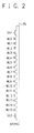
- Fig. 2 is a view showing an equivalent circuit of the memory portion of the NAND flash memory having the arrangement shown in Figs. 1A and 1B.
- the drain and gate of the first select gate transistor are connected to a bit line BL and the control signal line SG1, respectively.
- the gate and source of the second select gate transistor are connected to the control signal line SG2 and the memory cell source ARVSS, respectively.
- the structure in which the first select gate transistor, a plurality of memory cell transistors, and the second select gate transistor are connected in series as shown in Fig. 2 is called a string.
- a number of such strings are connected to one bit line.
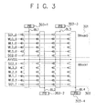
- Fig. 3 is a view showing the arrangement of a memory cell array of a NAND flash memory.
- Fig. 3 shows a NAND flash memory composed of strings each made up of a first select gate transistor, four memory cell transistors, and a second select gate transistor.
- reference numeral 301 denotes a first block composed of four strings connected to the memory cell source line ARVSS at one end and to first to fourth bit lines BL1 to BL4 at the other end.
- reference numeral 302 denotes a second block composed of four strings, different from those constructing the first block, connected to the memory cell source line ARVSS at one end and to the first to fourth bit lines BL1 to BL4 at the other end.
- Reference numerals 303-1, 303-2, 303-3, and 303-4 denote page buffers connected to the first, second, third, and fourth bit lines BL1, BL2, BL3, and BL4, respectively. These page buffers 303-1 to 303-4 control the potentials of the bit lines BL1 to BL4 in order to write data supplied to memory cell transistors, and output data to the outside on the basis of the potentials of the bit lines BL1 to BL4.
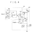
- Fig. 4 is a block diagram showing the arrangement of each of the page buffers 303-1 to 303-4 shown in Fig. 3.
- this page buffer includes a sense amplifier unit 401 and a latch buffer unit 411.
- the sense amplifier unit 401 comprises one P-channel MOS transistor (to be referred to as a "Pch-Tr” hereinafter) 402, and five N-channel MOS transistors (to be referred to as "Nch-Tr's" hereinafter) 403, 404, 405, 406, and 407.
- Pch-Tr P-channel MOS transistor
- Nch-Tr's N-channel MOS transistors
- a power supply voltage Vcc is supplied to the source of the Pch-Tr 402, and the gate and drain of this Pch-Tr 402 are connected to a signal line PBIAS and the drain of the Nch-Tr 403, respectively.
- the gate and source of the Nch-Tr 403 are connected to a signal line BLCTL and the drain of the Nch-Tr 404, respectively.
- the gate and source of this Nch-Tr 404 are connected to a signal line BLPRT and the bit line BL, respectively.
- the drain, gate, and source of the Nch-Tr 405 are connected to a node NB (to be described later), an interconnecting point SNS between the drains of the Pch-Tr 402 and the Nch-Tr 403, and the drain of the Nch-Tr 406, respectively.
- the gate and source of the Nch-Tr 406 are connected to a signal line SET and a ground potential (GND), respectively.
- the drain, gate, and source of the Nch-Tr 407 are connected to a node NA (to be described later), a signal line PGMON, and an interconnecting point between the drains of the Pch-Tr 402 and the Nch-Tr 403, respectively.
- the latch buffer unit 411 comprises two inverters 412 and 413, two Pch-Tr's 414 and 415, and four Nch-Tr's 416, 417, 418, and 419.
- the node NA is connected to the input terminal of the inverter 412, and the node NB is connected to the output terminal of the inverter 412.
- This node NB is also connected to the input terminal of the inverter 413, and the node NA is connected to the output terminal of the inverter 413. That is, these inverters 412 and 413 construct a latch circuit.
- the power supply voltage Vcc is supplied to the source of the Pch-Tr 414, and the gate and drain of this Pch-Tr 414 are connected to the node NA and the source of the Pch-Tr 415, respectively.
- the gate and drain of the Pch-Tr 415 are connected to a signal line LD and the drain of the Nch-Tr 416, respectively.
- the gate and source of this Nch-Tr 416 are connected to a signal line RD and the drain of the Nch-Tr 417, respectively.
- the gate and source of the Nch-Tr 417 are connected to the node NA and the ground potential (GND), respectively.
- the source, gate, and drain of the Nch-Tr 418 are connected to a signal line PBOUT, a signal line YD, and an interconnecting point between the drains of the Pch-Tr 415 and the Nch-Tr 416, respectively.
- the source, gate, and drain of the Nch-Tr 419 are connected to an interconnecting point between the drains of the Pch-Tr 415 and the Nch-Tr 416, the signal line LD, and the node NA, respectively.
- This Nch-Tr 418 is controlled on the basis of a signal corresponding to an address from which data supplied via the signal line YD is to be read out, and outputs the signal formed by inverting the signal at the node NA via the signal line PBOUT. In this manner, it is possible to prevent the inversion, due to the external wiring capacitance (signal line PBOUT) or the like, of data in the latch circuit composed of the inverters 412 and 413, before this data in the latch circuit is determined. Note that the operation between the bit line BL and the node NA in the latch buffer unit 411 during data read will be described later.
- Fig. 5A is a schematic view showing the state of the memory cell transistor when "1" is stored as a data value.
- this memory cell transistor is an Nch-Tr having a control gate 501, a floating gate 502, an oxide film (tunnel oxide film) 503, and a diffusion layer 504.
- a threshold voltage V th of this memory cell transistor is negative, so the memory cell transistor functions as a depletion type (normally ON type) transistor.
- Fig. 5B is a schematic view showing the state of the memory cell transistor when "0" is stored as a data value.
- a read operation, program (data write) operation, program verify operation, and erase verify operation of the NAND flash memory will be explained in turn.
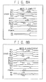
- Figs. 6A and 6B are timing charts of the read operation of the NAND flash memory.
- this word line WL0 is set at 0 V, and word lines other than the word line WL0 are set at about 4 V.
- the control signals SG1 and SG2 of a string having the memory cell from which the data value is to be read out are set at about 4 V, thereby selecting the string having this memory cell from which the data value is to be read out.
- the memory cell source line ARVSS is set at 0 V. Consequently, in the string having the memory cell from which the data value is to be read out, memory cells except for the memory cell to be selected by the word line WL0 and the first and second select gate transistors are turned on. Note that the signals SET and PGMON are set at 0 V.
- the signals BLCTL and BLPRT are set at HIGH level (to be referred to as "H” hereinafter) to turn on the Nch-Tr's 403 and 404 in the sense amplifier unit 401, thereby making the latch buffer unit 411 and the bit line BL electrically connectable.
- the signal PBIAS is set at LOW level (to be referred to as "L” hereinafter) to turn on the Pch-Tr 402, supplying an electric current to the bit line BL. This electric current is the reference for checking whether the data value of the memory cell is "1" or "0".
- the nodes NA and NB in the latch buffer unit 411 are set at "L” and "H", respectively.
- the signal SET is pulsed to "H". Since the potential at the interconnecting point SNS is "L”, the Nch-Tr 405 is OFF. Hence, even when the signal SET is pulsed to "H", the node NB in the latch buffer unit 411 maintains "H”. When the signal SET returns to "L”, therefore, the nodes NA and NB in the latch buffer unit 411 are "L” and “H”, respectively, so the state in which the data value is "1" is held in the latch circuit (Fig. 6A).
- the threshold voltage V th of this memory cell is positive.
- the word line WL0 is at 0 V, the memory cell from which the data value is to be read out is turned off, so no electric current flows. This raises (charges to "H") the potential at the interconnecting point SNS electrically connected to the bit line BL.
- the signals BLCTL and BLPRT are set at 0 V and PBIAS is set at Vcc to disconnect the electrical connection between the page buffer and the bit line BL. Additionally, all the word lines WLn and the control signals SG1 and SG2 are set at 0 V to select no string, thereby completing the read operation.
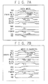
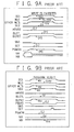
- Figs. 7A and 7B are timing charts of the program operation of the NAND flash memory.
- a string having a memory cell to be subjected to this program operation is selected by setting the control signals SG1 and SG2 of this string at the power supply voltage Vcc and 0 V, respectively.
- the memory cell source line ARVSS is set at the power supply voltage Vcc.
- the signal SET is set at 0 V.
- control is performed as described above with reference to Fig. 4 to set the nodes NA and NB in the latch buffer unit 411 at “L” and “H”, respectively.
- control is performed as described above with reference to Fig. 4 to set the nodes NA and NB in the latch buffer unit 411 at "H” and "L”, respectively.
- the signals BLCTL, BLPRT, and PGMON are changed to "H" to turn on the Nch-Tr's 403, 404, and 407 in the sense amplifier unit 401, thereby making the latch buffer unit 411 and the bit line BL electrically connectable.
- the word line WL0 is set at a voltage of 15 to 20 V (e.g., 18 V), and word lines other than this word line WL0 are set at about 10 V.
- the potential at the interconnecting point SNS i.e., the potential of the bit line BL is set at 0 V ("L") by that voltage level set at the node NA in the latch buffer unit 411, which is supplied via the Nch-Tr 407. Consequently, the control gate of the memory cell into which the data is to be written is set at 15 to 20 V, and the diffusion layer is set at 0 V. This potential difference of 15 to 20 V between the control gate and the diffusion layer injects electrons into the floating gate from the memory cell channel portion, writing a data value "0" in the memory cell (Fig. 7A).
- the potential at the interconnecting point SNS i.e., the potential of the bit line BL is set at "H" by that voltage level set at the node NA in the latch buffer unit 411, which is supplied via the Nch-Tr 407. Consequently, a voltage of 15 to 20 V is applied to the control gate of the memory cell selected by the word line WL0. Since, however, the diffusion layer is "H", no electrons are injected into the floating gate from the memory cell channel portion, so no data is written in the memory cell (Fig. 7B).
- the signals BLCTL, BLPRT, and PGMON are set at 0 V to disconnect the electrical connection between the bit line BL and the page buffer. Additionally, all the word lines WLn and the control signals SG1 and SG2 are set at 0 V to select no string. Furthermore, the memory cell source line ARVSS is set at 0 V to complete the program operation.
- the memory cell source line is set at the power supply voltage Vcc.
- a voltage lower than this power supply voltage Vcc can also be used if it can prohibit that the voltage levels at the nodes NA and NB of the latch buffer unit 411 can be inverted.
- This voltage is preferably substantially 1/2 the power supply voltage Vcc or more, and less than the power supply voltage Vcc.
- Figs. 8A and 8B are timing charts of the program verify operation of the NAND flash memory.
- the basic operation of this program verify operation is the same as the read operation described above, except that in the program verify operation the word line WL0 to be selected is set at a certain positive potential. For example, when the word line WL0 is set at 0.8 V, a read margin of 0.8 V can be obtained with respect to the minimum threshold voltage V th of a memory cell from which the data value "0" is to be read out in the read operation.
- the voltage levels at the nodes NA and NB in the latch buffer unit 411 are those of these nodes NA and NB at the end of the program operation. That is, the voltage levels at the nodes NA and NB in the latch buffer unit 411 are "L” and “H”, respectively, when data is written in a memory cell, and "H” and “L”, respectively, when data write to a memory cell is inhibited.
- the condition by which it is determined by the program verify operation that the program operation is normally performed is that the nodes NA and NB in the latch buffer unit 411 are "H” and "L", respectively. Additionally, in the NAND flash memory the program verify operation is performed for all memory cells sharing the same word line at the same time. Therefore, when the nodes NA and NB in the latch buffer unit 411 of each of all page buffers are "H" and "L", respectively, it is determined that the program operation is normally done in the NAND flash memory.
- the word line WL0 is set at 0.8 V, and word lines other than this word line WL0 are set at about 4 V.
- the control signals SG1 and SG2 of a string having a memory cell to be subjected to program verify are set at about 4 V, thereby selecting this string having the memory cell to be subjected to program verify.
- the memory cell source line ARVSS is set at 0 V. Consequently, in the string having the memory cell to be subjected to program verify, memory cells except for this memory cell to be selected by the word line WL0 and the first and second select gate transistors are turned on. Note that the signals SET and PGMON are set at 0 V.
- the signals BLCTL and BLPRT are changed to "H” and the signal PBIAS is changed to "L” to turn on the Pch-Tr 402 and the Nch-Tr's 403 and 404 in the sense amplifier unit 401, thereby making the latch buffer unit 411 and the bit line BL electrically connectable and supplying an electric current to the bit line BL.
- This electric current is the reference for checking whether data (the data value "0") is well written in the memory cell (whether the memory cell has a sufficient read margin).
- the threshold value V th of this memory cell is higher than 0.8 V of the word line WL0. Therefore, the memory cell is turned off, so no electric current flows. This raises (charges to "H") the potential at the interconnecting point SNS electrically connected to the bit line BL and turns on the Nch-Tr 405.
- the memory cell threshold value V th is lower than 0.8 V of the word line WL0. Therefore, the memory cell is turned on, and an electric current flows. This lowers (to "L") the potential at the interconnecting point SNS electrically connected to the bit line BL.
- the signal SET is pulsed to "H". Since the potential at the interconnecting point SNS is "L”, the Nch-Tr 405 is OFF. Hence, even if the signal SET is pulsed to "H", the node NB in the latch buffer unit 411 maintains "H". When the signal SET returns to "L”, therefore, the nodes NA and NB in the latch buffer unit 411 are still "L” and “H", respectively, so it is determined that the data is not well written in the memory cell, i.e., the program operation failed (Fig. 8B).
- the signals BLCTL and BLPRT are set at 0 V and PBIAS is set at Vcc to disconnect the electrical connection between the page buffer and the bit line BL. Additionally, all the word lines WLn and the control signals SG1 and SG2 are set at 0 V to select no string, thereby completing the program verify operation.
- this program verify operation is terminated. After that, the program operation and the program verify operation are repeatedly performed for the memory cell until it is determined that the data is well written in the memory cell.
- the threshold voltage V th of a memory cell to which no data write is permitted is lower than 0.8 V of the word line WL0, so this memory cell is turned on to allow an electric current to flow. Since this lowers the potential at the interconnecting point SNS, i.e., the potential of the bit line BL, the Nch-Tr 405 is turned off. Therefore, even when the signal SET is pulsed to "H” and then returned to "L", the nodes NA and NB in the latch buffer unit 411 maintain "H” and "L”, respectively. Accordingly, it is determined that the program operation is normally performed, so the program verify operation is completed.
- the program operation is performed by setting the nodes NA and NB in the latch buffer unit 411 at "H” and "L", respectively.
- a string having a memory cell to be subjected to a program operation is selected, and the memory cell source line ARVSS is set at the power supply voltage Vcc. Note that the signal SET is set at 0 V.
- the signals BLCTL, BLPRT, and PGMON are changed to "H” to make the latch buffer unit 411 and the bit line BL electrically connectable. Since the nodes NA and NB in the latch buffer unit 411 are "H” and “L", respectively, and the memory cell source line ARVSS short-circuited to the bit line BL is "H" (the power supply voltage Vcc), the potential at the interconnecting point SNS, i.e., the potential of the bit line BL changes to "H".
- the memory cell source line ARVSS is set at the power supply voltage Vcc in the period during which the program operation is performed. Therefore, the potential of the bit line BL is kept "H” if this bit line BL and the memory cell source line ARVSS are short-circuited. Consequently, a program verify operation performed after the program operation determines that the program operation is normally done, so this program verify operation can be terminated.
- Figs. 10A and 10B are timing charts of the erase verify operation of the NAND flash memory.
- the basic operation of this erase verify operation is the same as the read operation described earlier, except that this erase verify operation is performed in a selected block (erase unit). That is, all the word lines WLn in this block are set at 0 V, and the memory cell source line ARVSS is set at a certain positive potential. In this way, the potential of the control gate with respect to the source of a memory cell is equivalently set at a negative potential, thereby ensuring the threshold voltage V th of this memory cell.
- a read margin of 0.6 V can be obtained with respect to the minimum threshold voltage V th (absolute value) of a memory cell from which the data value "1" is to be read out in the read operation.
- the condition by which it is determined that data in a memory cell is normally erased is that the nodes NA and NB in the latch buffer circuit 411 are "L” and "H", respectively.
- all the word lines WLn in a selected block are set at 0 V, and the control signals SG1 and SG2 of a string included in the block are set at about 4 V.
- the memory cell source line ARVSS is set at 0.6 V. Note that the signals SET and PGMON are set at 0 V.
- the signals BLCTL and BLPRT are changed to "H” and the signal PBIAS is changed to "L” to turn on the Pch-Tr 402 and the Nch-Tr's 403 and 404 in the sense amplifier 401, thereby making the latch buffer unit 411 and the bit line BL electrically connectable and supplying an electrical current to the bit line BL.
- This electric current is the reference for checking whether data in a memory cell is well erased.
- the signal BLCTL is set at about 1 V. In this erase verify operation, however, the signal BLCTL is set at about 1.6 V (when the memory cell source line ARVSS is 0.6 V). This is to supply a sufficient drain-source voltage to each of a plurality of memory cells in the string.
- the nodes NA and NB in the latch buffer circuit 411 are set at "L” and "H", respectively.
- the threshold voltage V th of this memory cell is lower than a potential difference of -0.6 V of the word line WLn from the memory cell source line ARVSS. Therefore, the memory cell is turned on, and an electric current flows. This lowers (to "L") the potential at the interconnecting point SNS electrically connected to the bit line BL.
- the signals BLCTL and BLPRT are set at 0 V and PBIAS is set at Vcc to disconnect the electrical connection between the page buffer and the bit line BL, and the control signals SG1 and SG2 are set at 0 V to select no string.
- the memory cell source line ARVSS is set at 0 V to complete this erase verify operation.
- the threshold voltage V th of this memory cell is higher than the potential difference of -0.6 V of the word line WLn from the memory cell source line ARVSS. Therefore, the memory cell is turned off, and no electric current flows. This raises (charges to "H") the potential at the interconnecting point SNS electrically connected to the bit line BL, and turns on the Nch-Tr 405.
- erase operation and erase verify operations are executed again. Note that the erase operation is performed by setting all the word lines WLn in a selected block at 0 V, supplying about 20 V to a well in which a memory cell is formed, and extracting electrons into this well from the floating gate of the memory cell.
- Fig. 11 shows examples of voltages supplied via the control signal lines SG1 and SG2, the word lines WL (a selected word line and non-selected word lines), and the memory cell source line ARVSS, and the corresponding voltages of the bit line BL, in the read operation, program operation, program verify operation, and erase verify operation described above.
- a positive voltage (a voltage which is in the range of approximately 1/2 of the power supply voltage Vcc to the power supply voltage Vcc) is supplied to the memory cell source line ARVSS at least during the period in which the signal PGMON for electrically connecting the node NA in the latch buffer unit 411 and the bit line BL is set at "H".
- the potential of a line for supplying a reference potenti al to a memory cell for storing data is set at a positive potential during a period in which data write to the memory cell is performed.
Landscapes
- Engineering & Computer Science (AREA)
- Microelectronics & Electronic Packaging (AREA)
- Read Only Memory (AREA)
- For Increasing The Reliability Of Semiconductor Memories (AREA)
- Non-Volatile Memory (AREA)
- Semiconductor Memories (AREA)
Abstract
Description
Claims (15)
- A semiconductor memory comprising:wherein during a period in which a data write operation to said memory cell is performed, a potential of said line for supplying the reference potential to said memory cell is set at a positive potential.a memory cell comprising a transistor having a control gate and a floating gate to store data;a line for supplying a reference potential to said memory cell; andmeans for supplying said reference potential to said line,
- The memory according to claim 1, wherein the positive potential is not more than a power supply voltage of said semiconductor memory and not less than 1/2 the power supply voltage.
- The memory according to claim 1 or 2, wherein during a period in which a program verify operation for checking data written by the data write operation is performed, the potential of said line for supplying the reference potential to said memory cell is set at 0 V.
- The memory according to claim 1, 2 or 3, wherein the positive potential is the power supply voltage of said semiconductor memory.
- The memory according to claim 1, 2 or 3, wherein the positive potential is substantially 1/2 the power supply voltage of said semiconductor memory.
- The memory according to any of the preceding claims, wherein a plurality of said memory cells are connected in series, one end of the series-connected memory cells is connected to a bit line for inputting and outputting data to and from said memory cells, and the other end of the series-connected memory cells is connected to said line for supplying the reference potential to said memory cells.
- The memory according to claim 6, wherein during a period in which a potential of said bit line is set at a potential corresponding to write data to said memory cells, the potential of said line for supplying the reference potential to said memory cells is set at a positive potential.
- The memory according to claim 7, wherein the positive potential is not more than a power supply voltage of said semiconductor memory and not less than 1/2 the power supply voltage.
- The memory according to claim 7 or 8, wherein during a period in which a program verify operation for checking data written by the data write operation is performed, the potential of said line for supplying the reference potential to said memory cells is set at 0 V.
- A method of driving a semiconductor memory which stores data in a memory cell comprising a transistor having a control gate and a floating gate,
the method comprising supplying a positive potential to a line for supplying a reference potential to the memory cell during a period in which a data write operation to the memory cell is performed. - The method according to claim 10, wherein the positive potential is not more than a power supply voltage of the semiconductor memory and not less than 1/2 the power supply voltage.
- The method according to claim 10 or 11, wherein during a period in which a program verify operation for checking data written by the data write operation is performed, 0 V is supplied to the line for supplying the reference potential to the memory cell.
- A method of driving a semiconductor memory which stores data in a memory cell comprising a transistor having a control gate and a floating gate, and in which a plurality of the memory cells are connected in series, one end of the series-connected memory cells is connected to a bit line for inputting and outputting data to and from the memory cells, and the other end of the series-connected memory cells is connected to a line for supplying a reference potential to the memory cells,
the method comprising supplying a positive potential to said line for supplying the reference potential to the memory cells during a period in which a potential of the bit line is set at a potential corresponding to write data to the memory cells. - The method according to claim 13, wherein the positive potential is not more than a power supply voltage of the semiconductor memory and not less than 1/2 the power supply voltage.
- The method according to claim 13 or 14, wherein during a period in which a program verify operation for checking data written by the data write operation is performed, 0 V is supplied to the line for supplying the reference potential to the memory cells.
Applications Claiming Priority (2)
| Application Number | Priority Date | Filing Date | Title |
|---|---|---|---|
| JP2001217660 | 2001-07-18 | ||
| JP2001217660A JP2003030994A (en) | 2001-07-18 | 2001-07-18 | Semiconductor storage device and method of driving semiconductor storage device |
Publications (2)
| Publication Number | Publication Date |
|---|---|
| EP1278200A2 true EP1278200A2 (en) | 2003-01-22 |
| EP1278200A3 EP1278200A3 (en) | 2005-06-01 |
Family
ID=19051942
Family Applications (1)
| Application Number | Title | Priority Date | Filing Date |
|---|---|---|---|
| EP02250788A Withdrawn EP1278200A3 (en) | 2001-07-18 | 2002-02-06 | Semiconductor memory and method of driving semiconductor memory |
Country Status (6)
| Country | Link |
|---|---|
| US (1) | US20030016560A1 (en) |
| EP (1) | EP1278200A3 (en) |
| JP (1) | JP2003030994A (en) |
| KR (1) | KR20030010474A (en) |
| CN (1) | CN1397951A (en) |
| TW (1) | TW546653B (en) |
Families Citing this family (13)
| Publication number | Priority date | Publication date | Assignee | Title |
|---|---|---|---|---|
| BRPI0400108B1 (en) | 2004-01-22 | 2017-03-28 | Empresa Brasileira De Compressores S A - Embraco | linear compressor and control method of a linear compressor |
| JP2007164231A (en) | 2005-12-09 | 2007-06-28 | Nec Electronics Corp | Semiconductor design support device |
| JP5050364B2 (en) * | 2006-02-13 | 2012-10-17 | サンケン電気株式会社 | Field effect semiconductor device and manufacturing method thereof |
| US7701770B2 (en) * | 2006-09-29 | 2010-04-20 | Hynix Semiconductor Inc. | Flash memory device and program method thereof |
| KR100851856B1 (en) * | 2006-12-11 | 2008-08-13 | 삼성전자주식회사 | Semiconductor memory device and repair method thereof |
| US9486109B2 (en) | 2011-07-14 | 2016-11-08 | Tsi Technologies Llc | Induction heating system employing induction-heated switched-circuit vessels |
| CN104979009B (en) * | 2014-04-02 | 2019-01-22 | 中芯国际集成电路制造(上海)有限公司 | Memory and its reading circuit |
| KR102124209B1 (en) * | 2014-04-14 | 2020-06-18 | 삼성전자주식회사 | Semiconductor memory device |
| US9830219B2 (en) * | 2014-09-15 | 2017-11-28 | Western Digital Technologies, Inc. | Encoding scheme for 3D vertical flash memory |
| KR102620813B1 (en) * | 2017-01-03 | 2024-01-04 | 에스케이하이닉스 주식회사 | Semiconductor device, operating method thereof and memory system |
| KR102679560B1 (en) * | 2018-10-25 | 2024-07-01 | 에스케이하이닉스 주식회사 | Storage device and operating method thereof |
| US10942799B1 (en) | 2019-09-06 | 2021-03-09 | Intel Corporation | Defective bit line management in connection with a memory access |
| CN110853694B (en) * | 2019-10-31 | 2022-02-11 | 西安紫光国芯半导体有限公司 | Repair method for NAND flash memory defects |
Family Cites Families (6)
| Publication number | Priority date | Publication date | Assignee | Title |
|---|---|---|---|---|
| US6108238A (en) * | 1997-09-11 | 2000-08-22 | Kabushiki Kaisha Toshiba | Programmable semiconductor memory device having program voltages and verify voltages |
| JPH11186419A (en) * | 1997-12-25 | 1999-07-09 | Toshiba Corp | Nonvolatile semiconductor memory device |
| US5978266A (en) * | 1998-02-17 | 1999-11-02 | Advanced Micro Devices, Inc. | Array VSS biasing for NAND array programming reliability |
| JP3866460B2 (en) * | 1998-11-26 | 2007-01-10 | 株式会社東芝 | Nonvolatile semiconductor memory device |
| JP3540640B2 (en) * | 1998-12-22 | 2004-07-07 | 株式会社東芝 | Nonvolatile semiconductor memory device |
| JP3888808B2 (en) * | 1999-08-16 | 2007-03-07 | 富士通株式会社 | NAND nonvolatile memory |
-
2001
- 2001-07-18 JP JP2001217660A patent/JP2003030994A/en not_active Withdrawn
-
2002
- 2002-01-30 TW TW091101593A patent/TW546653B/en active
- 2002-01-31 US US10/059,354 patent/US20030016560A1/en not_active Abandoned
- 2002-02-06 EP EP02250788A patent/EP1278200A3/en not_active Withdrawn
- 2002-02-20 KR KR1020020008904A patent/KR20030010474A/en not_active Withdrawn
- 2002-03-14 CN CN02107312A patent/CN1397951A/en active Pending
Also Published As
| Publication number | Publication date |
|---|---|
| US20030016560A1 (en) | 2003-01-23 |
| JP2003030994A (en) | 2003-01-31 |
| EP1278200A3 (en) | 2005-06-01 |
| CN1397951A (en) | 2003-02-19 |
| KR20030010474A (en) | 2003-02-05 |
| TW546653B (en) | 2003-08-11 |
Similar Documents
| Publication | Publication Date | Title |
|---|---|---|
| US7483301B2 (en) | Nonvolatile memory devices that support virtual page storage using odd-state memory cells and methods of programming same | |
| US6788601B2 (en) | Semiconductor memory device and current mirror circuit | |
| JP4908149B2 (en) | NAND flash memory | |
| EP1039388B1 (en) | Block erasable semiconductor memory device with defective block replacement | |
| US8400837B2 (en) | Semiconductor memory device with memory cells having charge accumulation layer | |
| US7898889B2 (en) | Nonvolatile semiconductor memory device | |
| JP2019160382A (en) | Nonvolatile semiconductor memory | |
| US5847995A (en) | Nonvolatile semiconductor memory device having a plurality of blocks provided on a plurality of electrically isolated wells | |
| EP1278200A2 (en) | Semiconductor memory and method of driving semiconductor memory | |
| US10510421B2 (en) | Semiconductor storage device and readout method thereof | |
| US8897068B2 (en) | Semiconductor memory device | |
| US7212443B2 (en) | Non-volatile memory and write method of the same | |
| US5684747A (en) | Method for erasing nonvolatile semiconductor memory device incorporating redundancy memory cells | |
| JP5631436B2 (en) | Semiconductor memory device | |
| JP2017079088A (en) | Nonvolatile semiconductor memory device | |
| US7782676B2 (en) | Method of operating a nonvolatile memory device | |
| JP3176011B2 (en) | Semiconductor storage device | |
| JP4012144B2 (en) | Semiconductor memory device | |
| US20100124128A1 (en) | Nand flash memory | |
| US8374041B2 (en) | Transfer circuit, nonvolatile semiconductor device using the same, and transfer method of the same | |
| US9275739B2 (en) | Semiconductor memory device, reading method, and programming method | |
| JP2002150797A (en) | Nonvolatile semiconductor memory device | |
| US20180144807A1 (en) | Semiconductor device | |
| JP2002245789A (en) | Non-volatile memory | |
| JP2006286033A (en) | Nonvolatile semiconductor memory device |
Legal Events
| Date | Code | Title | Description |
|---|---|---|---|
| PUAI | Public reference made under article 153(3) epc to a published international application that has entered the european phase |
Free format text: ORIGINAL CODE: 0009012 |
|
| AK | Designated contracting states |
Kind code of ref document: A2 Designated state(s): AT BE CH CY DE DK ES FI FR GB GR IE IT LI LU MC NL PT SE TR |
|
| AX | Request for extension of the european patent |
Free format text: AL;LT;LV;MK;RO;SI |
|
| PUAL | Search report despatched |
Free format text: ORIGINAL CODE: 0009013 |
|
| AK | Designated contracting states |
Kind code of ref document: A3 Designated state(s): AT BE CH CY DE DK ES FI FR GB GR IE IT LI LU MC NL PT SE TR |
|
| AX | Request for extension of the european patent |
Extension state: AL LT LV MK RO SI |
|
| STAA | Information on the status of an ep patent application or granted ep patent |
Free format text: STATUS: THE APPLICATION IS DEEMED TO BE WITHDRAWN |
|
| AKX | Designation fees paid | ||
| 18D | Application deemed to be withdrawn |
Effective date: 20050901 |
|
| REG | Reference to a national code |
Ref country code: DE Ref legal event code: 8566 |