JP3866460B2 - Nonvolatile semiconductor memory device - Google Patents
Nonvolatile semiconductor memory device Download PDFInfo
- Publication number
- JP3866460B2 JP3866460B2 JP26617699A JP26617699A JP3866460B2 JP 3866460 B2 JP3866460 B2 JP 3866460B2 JP 26617699 A JP26617699 A JP 26617699A JP 26617699 A JP26617699 A JP 26617699A JP 3866460 B2 JP3866460 B2 JP 3866460B2
- Authority
- JP
- Japan
- Prior art keywords
- memory cell
- block
- nand
- signal line
- data
- Prior art date
- Legal status (The legal status is an assumption and is not a legal conclusion. Google has not performed a legal analysis and makes no representation as to the accuracy of the status listed.)
- Expired - Lifetime
Links
Images


Classifications
-
- H—ELECTRICITY
- H10—SEMICONDUCTOR DEVICES; ELECTRIC SOLID-STATE DEVICES NOT OTHERWISE PROVIDED FOR
- H10B—ELECTRONIC MEMORY DEVICES
- H10B69/00—Erasable-and-programmable ROM [EPROM] devices not provided for in groups H10B41/00 - H10B63/00, e.g. ultraviolet erasable-and-programmable ROM [UVEPROM] devices
-
- G—PHYSICS
- G11—INFORMATION STORAGE
- G11C—STATIC STORES
- G11C16/00—Erasable programmable read-only memories
- G11C16/02—Erasable programmable read-only memories electrically programmable
- G11C16/04—Erasable programmable read-only memories electrically programmable using variable threshold transistors, e.g. FAMOS
- G11C16/0483—Erasable programmable read-only memories electrically programmable using variable threshold transistors, e.g. FAMOS comprising cells having several storage transistors connected in series
-
- G—PHYSICS
- G11—INFORMATION STORAGE
- G11C—STATIC STORES
- G11C16/00—Erasable programmable read-only memories
- G11C16/02—Erasable programmable read-only memories electrically programmable
- G11C16/06—Auxiliary circuits, e.g. for writing into memory
- G11C16/10—Programming or data input circuits
- G11C16/14—Circuits for erasing electrically, e.g. erase voltage switching circuits
- G11C16/16—Circuits for erasing electrically, e.g. erase voltage switching circuits for erasing blocks, e.g. arrays, words, groups
-
- G—PHYSICS
- G11—INFORMATION STORAGE
- G11C—STATIC STORES
- G11C8/00—Arrangements for selecting an address in a digital store
- G11C8/14—Word line organisation; Word line lay-out
Description
【0001】
【発明の属する技術分野】
この発明は、電気的書き換え可能な複数のメモリセルを直列接続してNANDセル(メモリセルストリング)を構成してなる不揮発性半導体記憶装置(EEPROM)に関する。
【0002】
【従来の技術】
電気的書き換えを可能としたEEPROMとして、従来より、NANDセル型EEPROMが知られている。NANDセル型EEPROMの1つのメモリセルは、半導体基板上に絶縁膜を介して浮遊ゲート(電荷蓄積層)と制御ゲートが積層されたスタック構造のトランジスタを有する。複数個のメモリセルは、隣接するもの同士でソース・ドレインを共有する形で直列接続されてNANDセルを構成する。このようなNANDセルがマトリクス配列されてメモリセルアレイが構成される。
【0003】
メモリセルアレイの列方向に並ぶNANDセルの一端側のドレインは、選択トランジスタを介してビット線に共通接続され、他端側ソースはやはり選択トランジスタを介して共通ソース線に接続される。メモリセルトランジスタのワード線及び選択トランジスタのゲート電極は、メモリセルアレイの行方向にそれぞれワード線(制御ゲート線)、選択ゲート線として共通接続される。
【0004】
このようなNANDセル型EEPROMは、例えば次のような文献▲1▼,▲2▼により知られている。
【0005】
▲1▼ K. -D. Suh et al., "A 3.3V 32Mb NAND Flash Memory with Incremental Step Pulse Programming Scheme," IEEE J. Solid-State Circuits, Vol.30, pp.1149-1156, Nov.1995
▲2▼ Y. Iwata et al., "A 35ns Cycle Time 3.3V Only 32Mb NAND Flash EEPROM," IEEE J. Solid-State Circuits, Vol.30, pp.1157-1164, Nov.1995.
図18は、NANDセル型EEPROMのメモリセルアレイのひとつのNANDセルブロックの構成を示している。複数個のメモリセルMは、それらのソース、ドレインを隣接するもの同士で共有する形で直列接続されてNANDセルが構成される。NANDセルの一端は選択トランジスタS1を介してビット線BLに、他端はやはり選択トランジスタS2を介して共通接地線に接続される。図18の横方向に並ぶメモリセルMの制御ゲートは、共通にワード線WLに接続される。選択トランジスタS1,S2のゲートも同様に選択ゲート線SSL,GSLに共通接続される。一つのワード線により駆動されるNANDセルの範囲がNANDセルブロックを構成している。
【0006】
通常、この様なNANDセルブロックがビット線方向に複数個配置されてメモリセルアレイが構成される。各NANDセルブロックはデータ消去の単位となっていわゆる一括消去が行われる。またNANDセルブロック内のひとつの選択されたワード線に沿うメモリセル列は1ページと呼ばれ、1ページがデータ読み出し及び書き込みの単位となる。
【0007】
メモリセルMは、例えばnチャネルの場合、浮遊ゲートに電子が注入されたしきい値が正の状態(Eタイプ状態)と、浮遊ゲートの電子が放出されたしきい値が負の状態(Dタイプ状態)とを二値に対応させることにより、データ記憶を行う。例えば、Dタイプ状態が“1”データの保持状態(消去状態)、Eタイプ状態が“0”データ保持状態(書き込み状態)というように定義される。また、“1”データを保持しているメモリセルのしきい値を正方向にシフトさせて“0”データを保持した状態に移行させる動作が「書き込み動作」、“0”データを保持しているメモリセルのしきい値を負方向にシフトさせて“1”データを保持した状態に移行させる動作が「消去動作」というように定義される。この明細書では、以下の説明をこの定義に従って行う。
【0008】
図19は、メモリセルアレイの選択されたNANDセルブロックでのデータ消去、読み出し及び書き込み動作の各部電位関係を示している。消去動作では、選択されたNANDセルブロックの全ワード線を0V、選択ゲート線SSL,GSL及びビット線BLをフローティング(F)とし、メモリセルのP型ウェルに高い正の消去電圧Vera(例えば、3ms、21Vの消去パルス)を与える。その結果、選択ブロックでは、ウェルとワード線の間に消去電圧がかかり、浮遊ゲートの電子がFN(Fowler-Nordheim )トンネル電流によりウェルに放出される。これにより、そのNANDセルブロック内のメモリセルは“1”の消去状態になる。
【0009】
このとき、非選択のNANDセルブロックでは、フローティング状態のワード線とウェルとの容量カップリングにより、消去パルスの影響を受けない。カップリング比は、フローティング状態のワード線に接続される容量から計算される。実際には、ポリシリコンのワード線とセル領域のPウェルとの容量が全容量に対して支配的であり、実測結果から求めたカップリング比は約0.9と大きく、これがFNトンネル電流が流れるのを妨げる。消去ベリファイ(検証)は選択ブロック内の全てのメモリセルのしきい値電圧が例えば−1V以下になったかどうかによって判定される。
【0010】
データ読み出し動作は、選択ワード線に0V、非選択ワード線及び選択ゲート線に一定の読み出し電圧Vread(しきい値によらず、チャネルを導通させるに必要な電圧)を与え、選択されたメモリセルの導通の有無によるビット線BLの電位変化を読むことにより行われる。
【0011】
データ書き込み動作は、選択ワード線に正の高い書き込み電圧Vpgm、非選択ワード線にはパス電圧Vpass、ビット線側の選択ゲート線SSLにVcc、共通ソース線側の選択ゲート線GSLにVss=0Vを与え、“0”を書き込むべきビット線BLにVss、書き込み禁止(即ち“1”の消去状態に保つべき)ビット線BLにVccを与えることにより行われる。このとき、Vssが与えられたビット線につながる選択メモリセルでは、チャネル電位がVssに保持され、制御ゲートとチャネル間の大きな電界がかかって、チャネルから浮遊ゲートにトンネル電流による電子注入が生じる。同じビット線につながるVpassが与えられた他の非選択メモリセルでは、書き込みに十分に電界がかからず、書き込みは行われない。
【0012】
Vccが与えられたビット線に沿うメモリセルでは、NANDセルのチャネルはVcc又はVcc−Vth(Vthは選択トランジスタのしきい値電圧)に予備充電されて選択トランジスタがカットオフする。そして制御ゲートに書き込み電圧Vpgm及びパス電圧Vpassが与えられると、フローティングとなっているNANDセルのチャネルと、Vpgm又はVpassが与えられた制御ゲートとの容量結合によりチャネル電位は上昇して、電子注入が起こらない。
【0013】
以上のようにして、Vssが与えられたビット線とVpgmが与えられた選択ワード線の交差部のメモリセルでのみ、電子注入が行われて“0”書き込みがなされる。選択ブロック内の書き込み禁止のメモリセルにおいては、上述のようにチャネル電位がワード線とチャネルとの容量結合によって決定されるから、書き込み禁止電位を十分に高くするためには、チャネルの初期充電を十分に行うことおよびワード線とチャネル間の容量カップリング比を大きくすることが重要となる。
【0014】
ワード線とチャネル間のカップリング比Bは、B=Cox/(Cox+Cj)により算出される。ここで、Coxはワード線とチャネルとの間のゲート容量の総和、Cjはメモリセルトランジスタのソースおよびドレインの接合容量の総和である。また、NANDセルのチャネル容量とは、これらゲート容量の総和Coxと接合容量の総和Cjの合計となる。さらに、その他の容量である選択ゲート線とソースのオーバラップ容量や、ビット線とソースおよびドレインとの容量等は全チャネル容量に比べて非常に小さいため、ここでは無視している。
【0015】
【発明が解決しようとする課題】
以上に説明したNAND型EEPROMにおいては、従来より平面方向(デザイン・ルール)のスケーリングは行われているが、これに対応した深さ方向(酸化膜厚)のスケーリングは行われていない。具体的に、トンネル酸化膜の膜厚は、16M、32M、64M、256MビットNAND型EEPROMで10nmとほぼ一定である。そしてトンネル酸化膜の膜厚が一定であれば、トンネル酸化膜にかかる電界を一定にするために、メモリセルの書き換え電圧も一定電圧を維持しなければならず、低電圧化できない。トンネル酸化膜の膜厚について、プロセス技術者によりさらに薄膜化することが試みられてはいるが、例えば、5nmの酸化膜は実現していない。また、書き換え電圧を低電圧化させるには、制御ゲートと浮遊ゲート間の容量を増大させ、カップリング比を大きくすれば良い。しかし、これも、制御ゲートと浮遊ゲート間の酸化膜を薄膜化させる必要があったり、制御ゲートと浮遊ゲートの間のキャパシタ面積を増やすなどの工夫が必要であり、容易には成し遂げ得ない。
【0016】
結局、NAND型EEPROMでは、16Mから256Mビットまで書き換え電圧として20V程度の高電圧が必要となっている。このため、その高電圧をワード線に駆動するロウデコーダのトランジスタを高耐圧トランジスタで設計しなくてはならない。高耐圧トランジスタは、周辺回路の通常のトランジスタよりもデザイン・ルールを緩くして、トランジスタ内の各部の寸法を長くすることにより、加わる電界を弱める工夫が成されている。例えば、0.25μmルールで設計した256MビットNAND型EEPROMの場合、この高耐圧トランジスタは、周辺回路の通常のトランジスタよりもデザイン・ルールを数倍大きくしている。そして、256MビットNAND型EEPROMの16個のメモリセルと2個の選択トランジスタから成る1つのNANDストリングのピッチ(長さ)は、8.5μmであり、そのピッチに2個以上の高耐圧トランジスタは配置できず、1個の高耐圧トランジスタを配置するのが限界となっている。
【0017】
例えば、次世代1GビットNAND型EEPROMでは、0.15μmのデザイン・ルールが適用された場合、この1つのNANDストリングのピッチは、約5um程度になる。また、縦方向のスケーリングがやはり困難であったとすると、上述した理由により書き換え電圧を低くすることができない。従って、現在の16個のメモリセルトランジスタと2個の選択トランジスタから成る1つのNANDストリングのピッチには、サイズの大きいワード線駆動用の高耐圧トランジスタを配置できない。このため、例えば、1つのNANDストリングの直列接続のメモリセルトランジスタの数を増やし、例えば、32個のメモリセル構成とか、64個のメモリセル構成とかして、1つのNANDストリングのピッチを大きくしなければならなくなる。
【0018】
しかし、単に1つのNANDストリング内のメモリセルトランジスタの個数を増やすと、同時に消去ブロックサイズが増えてしまう。それは、従来のNAND型EEPROMでは、NANDストリング(NANDセル)を1ブロックとし、ブロック単位での消去しか許されなかったためである。NANDセルブロック単位での消去しか許されない理由は、次の通りである。例えば、16個のメモリセルからなるNANDストリングを8個ずつのメモリセルを書き換えの単位である1ブロックとし、下部ブロックを何度も選択して書き換えたとする。そうすると、上部ブロックのワード線にはパス電圧Vpassのストレスが加わり、書き換えが多数回に及ぶと、非選択ブロックのしきい値電圧も変化してしまう。
【0019】
この消去ブロックのサイズは、16MビットNAND型EEPROMでは、4Kバイト、32MビットNAND型EEPROMでは、8Kバイト、256MビットNAND型EEPROMでは、16Kバイトと大容量化に伴い、徐々に大きくはなっている。しかし、例えば、デジタルカメラのフィルム媒体にNAND型EEPROMを使用した場合、コンパティビリティを保つために急激なブロックサイズの増大はしたくないという要請もある。したがって、大容量の1GビットNAND型EEPROMでも、256MビットNAND型EEPROMと同様に消去ブロックサイズを16Kバイトとする必要が出てくる。
【0020】
この発明は、上記事情を考慮してなされたもので、1つのNANDセルブロック内に複数の消去単位を設定可能としたNAND型EEPROMを提供することを目的としている。
【0021】
【課題を解決するための手段】
この発明による不揮発性半導体記憶装置の第1の態様は、第1の信号線と、第2の信号線と、これら第1の信号線と第2の信号線の間に電気的書き換え可能なメモリセルを複数個直列接続して構成されたNANDセルと、このNANDセルを複数ブロックに分割するためにNANDセル内の所定の隣接メモリセルの間に介在させたブロック分離選択トランジスタと、を有することを特徴とする。
【0022】
なお、この発明においては、複数ブロック間の少なくとも2つ以上のブロック分離選択トランジスタのゲートが共通接続されていても良い。
【0023】
また、この発明による不揮発性半導体記憶装置の第2の態様は、ワード線により選択される電気的書き換え可能なメモリセルが第1の信号線と第2の信号線の間にそれぞれ選択トランジスタを介して複数個直列接続されてNANDセルを構成して、複数のNANDセルが配列されたメモリセルアレイと、アドレスにより前記メモリセルアレイのメモリセル選択を行うアドレスデコーダと、前記メモリセルアレイからの読み出しデータをセンスし、前記メモリセルアレイへの書き込みデータをラッチする機能を有するセンスアンプ回路と、前記メモリセルアレイへのデータ書き込み、消去及び読み出しの制御を行う制御回路とを備え、前記メモリセルアレイは、各NANDセル内の所定の隣接メモリセルの間に介在させたブロック分離選択トランジスタにより複数のメモリセルユニットに分割されていることを特徴とする。
【0024】
なお、この発明において、具体的には、前記メモリセルアレイのデータ書き換え時、前記複数のメモリセルユニットの一つを消去単位として選択してデータ消去がなされ、1本のワード線に沿った複数のメモリセルの所定範囲を1ページとしてデータ書き込みがなされる。
【0025】
なおこの発明において、データ消去は、選択されたメモリセルユニットの全ワード線に接地電位を与え、非選択のメモリセルユニットの全ワード線、前記第1の信号線側及び第2の信号線側の選択トランジスタ及び前記ブロック分離選択トランジスタのゲートにそれぞれつながる選択ゲート線をフローティングとし、且つ前記メモリセルアレイが形成された基板領域に消去電圧を与えることにより行われる。
【0026】
なおこの発明において、データ書き込みは、書き込むべきデータ“0”,“1”に応じて第1の信号線に接地電位、電源電位を与え、選択されたメモリセルユニット内の非選択ワード線にメモリセルを導通させるパス電圧を与え、非選択のメモリセルユニットの全ワード線、及び非選択のメモリセルユニットと前記選択されたメモリセルユニットの間の前記ブロック分離選択トランジスタのゲートにつながる選択ゲート線にメモリセルを導通させる前記パス電圧より低い読み出し電圧を与え、前記選択されたメモリセルユニットの選択ワード線に前記パス電圧より高い書き込み電圧を与えることにより行われる。
【0027】
なおこの発明において、具体的には、前記メモリセルアレイは、各NANDセル内の所定の隣接メモリセルの間に介在させた2n −1(n:正の整数)個のブロック分離選択トランジスタにより、2n 個のメモリセルユニットに分割される。この場合、各メモリセルユニットが同数のメモリセルを含むようにしてもよいし、或いは異なる数のメモリセルを含むようにしてもよい。
【0028】
なおこの発明において好ましくは、前記アドレスデコーダのなかのワード線駆動回路は、前記メモリセルアレイのワード線方向の両端部に、1乃至2メモリセルユニット毎に振り分けて配置される。
【0029】
また、この発明による不揮発性半導体記憶装置の第3の態様は、それぞれ異なるワード線により選択される電気的書き換え可能な複数のメモリセルがビット線に直列接続されてNANDセルを構成し、ワード線方向に並ぶ複数のNANDセルがNANDセルブロックを構成し、且つ各NANDセルの所定の隣接メモリセルの間に介在させたブロック分離選択トランジスタにより前記NANDセルブロックが複数のメモリセルユニットに分割されたメモリセルアレイと、アドレスにより前記メモリセルアレイのメモリセル選択を行うアドレスデコーダと、前記メモリセルアレイからの読み出しデータをセンスし、前記メモリセルアレイへの書き込みデータをラッチする機能を有するセンスアンプ回路と、前記複数のメモリセルユニットの一つを消去単位として選択してそのメモリセルユニット内のデータを一括消去し、1本のワード線に沿った複数のメモリセルの所定範囲を1ページとしてデータ書き込みを行うデータ書き換え手段と、を備えたことを特徴とする。
【0030】
この発明によると、NANDセル内のブロック分離選択トランジスタを介在させることによって、1NANDセルブロック内に複数の消去ブロックを設定することが可能であり、消去ブロックサイズを増やすことなく、1NANDストリング内のメモリセルの個数を増やすことを可能となる。
【0031】
また、この発明による不揮発性半導体記憶装置の第4の態様は、第1および第2の信号線と、第1および第2の選択トランジスタと、各々が、電気的に書き換え可能なメモリセルを複数個直列接続して構成された第1乃至第n(n≦3)のNANDセルブロックと、第1乃至第(n−1)のブロック分離選択トランジスタと、を備え、前記第1の信号線に前記第1の選択トランジスタが接続され、前記第1の選択トランジスタに前記第1のNANDセルブロックが接続され、第i(1≦i≦n−1)のNANDセルブロックに第iのブロック分離選択トランジスタが接続され、第i(1≦i≦n−1)のブロック分離選択トランジスタに第(i+1)のNANDセルブロックが接続され、第nのNANDセルブロックに第2の選択トランジスタが接続され、第2の選択トランジスタに第2の信号線が接続され、前記第1乃至第nのブロック分離選択トランジスタのうち、少なくとも2つのブロック分離選択トランジスタのゲートが共通接続されていることを特徴とする。
【0032】
また、この発明による不揮発性半導体記憶装置の第5の態様は第1および第2の信号線と、第1および第2の選択トランジスタと、各々が電気的に書き換え可能な第1乃至第nのメモリセルと、第1乃至第(n−1)のブロック分離選択トランジスタと、を備え、前記第1の信号線に前記第1の選択トランジスタが接続され、前記第1の選択トランジスタに前記第1のメモリセルが接続され、第i(1≦i≦n−1)のメモリセルに第iのブロック分離選択トランジスタが接続され、第i(1≦i≦n−1)のブロック分離選択トランジスタに第(i+1)のメモリセルが接続され、第nのメモリセルに第2の選択トランジスタが接続され、第2の選択トランジスタに第2の信号線が接続され、前記第1乃至第nのブロック分離選択トランジスタのうち、少なくとも2つのブロック分離選択トランジスタのゲートが共通接続されていることを特徴とする。
【0033】
なお、第4および第5の態様において前記第1および第2の選択トランジスタのゲートは、多結晶シリコン、多結晶シリコンとシリサイドとの積層体、若しくは金属電極から構成され、前記第1乃至第(n−1)のブロック分離選択トランジスタのゲートは多結晶シリコン、多結晶シリコンとシリサイドとの積層体、若しくは金属電極から構成されていても良い。
【0034】
なお、第4および第5の態様において、前記第1および第2の選択トランジスタのゲートは、多結晶シリコン、多結晶シリコンとシリサイドとの積層体、若しくは、金属電極から構成され、前記第1乃至第(n−1)のブロック分離選択トランジスタのゲートは、多結晶シリコン、多結晶シリコンとシリサイドとの積層体、若しくは、金属電極から構成されるように構成しても良い。
【0035】
なお、データ書き込み時に、前記第1の選択トランジスタおよび前記第1乃至第(n−1)のブロック分離選択トランジスタのゲートには、電源電圧Vcc若しくはそれ以上の読み出し電圧Vreadが印加され、前記第2の選択トランジスタのゲートには、接地電圧Vssが印加されるように構成しても良い。
【0036】
なお、前記第1の信号線はビット線で、前記第2の信号線はセルソース線であることが好ましい。
【0037】
なお、前記メモリセルは浮遊ゲートと、前記浮遊ゲート上に絶縁膜を介して形成された制御ゲートと、を有する二層のスタック構造からなる電気的書き換え可能なメモリセルであることが好ましい。
【0038】
【発明の実施の形態】
第1の実施の形態
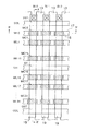
図1は、この発明の第1の実施の形態によるNAND型EEPROMのメモリセルアレイの1つのNANDセルブロック1のメモリセルアレイの等価回路を示している。この例では、ビット線BLの本数として528バイト((512+16)×8=4224本)を例にとり、示している。この実施の形態では、1つのNANDセルは32個のメモリセルトランジスタMC0〜MC31により構成されている。メモリセルトランジスタMC0〜MC31はビット線BLとソース線SLの間に直列接続される。ビット線BLとメモリトランジスタMC0の間には選択トランジスタSSTが設けられ、ソース線SLとメモリセルトランジスタMC31の間にも同様に選択トランジスタGSTが設けられている。
【0039】
この実施の形態においては、上述した二つの選択トランジスタSST,GSTの他に、1つのNANDセルを2分割する形でブロック分離のための選択トランジスタSTが設けられている。即ち、隣接するメモリセルトランジスタMC15とMC16の間にブロック分離選択トランジスタSTを介在させることにより、NANDブロック1が二つのメモリユニットMU0,MU1に分割されている。この2分割されたメモリユニットMU0,MU1がそれぞれデータ消去の単位ブロックサイズとなる。
【0040】
図2は、NANDセルブロック1のレイアウトであり、図3及び図4はそれぞれ、図2のA−A′、B−B′断面を示している。p型シリコン基板10のメモリセルアレイ領域にはn型ウェル11が形成され、このn型ウェル11内にはp型ウェル12が形成され、このp型ウェル12には素子分離絶縁膜13により素子領域が区画されている。素子領域にトンネル酸化膜14を介して浮遊ゲート15が各メモリセルトランジスタ毎に形成され、この上に層間ゲート絶縁膜16を介して制御ゲート17が形成されている。
【0041】
制御ゲート17は、図2に示すように行方向に連続的に配設されて、これがワード線WLとなる。制御ゲート17をマスクとしてイオン注入を行うことにより、ソース、ドレイン拡散層21が形成されている。図3では、選択トランジスタSST,STは、メモリセルトランジスタMCと同様の構造として示しているが、図4の断面に対応する断面では、浮遊ゲート15に対応する層と制御ゲート17に対応する層とが、所定箇所で共通接続されて連続的に配設されて、選択ゲート線SSL,STLとなる。ソース側の選択トランジスタGSTも同様であり、そのゲートは連続的に配設されて、選択ゲート線GSLとなる。ここで、選択トランジスタSST,STとメモリセルトランジスタMCとはゲート酸化膜厚を異ならせてもよい。
【0042】
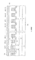
ページ書き込み/読み出し機能を持つNAND型EEPROMとしての全体ブロック構成は、図5のようになる。図示のように、メモリセルアレイ51と、外部から入力されたアドレスに基いてメモリセルアレイ51のワード線を選択駆動するロウデコーダ52と、メモリセルアレイ51のビット線BLに接続される、入出力データのラッチ機能を持つセンスアンプ回路53とを有する。センスアンプ回路53にはカラムゲート55が接続され、カラムデコーダ54により外部から入力されたアドレスに基いてカラムゲート55を制御することで、対応するビット線およびセンスアンプ回路が選択される。
【0043】
センスアンプ回路53は、カラムゲート55を介してデータ入出力(I/O)バッファ58に接続される。書き込み動作や消去動作に必要な高電圧を供給するために昇圧回路56が設けられ、またメモリセルアレイ51へのデータ書き込み、消去及び読み出しの制御信号を生成してチップ内部を制御するとともに外部とのインターフェースをとるための制御回路57が設けられている。
【0044】
ロウデコーダ52は、データの書き込み時、消去時およびデータの読み出し時にそれぞれアドレス信号に基づいて複数のワード線WLを選択駆動するものであり、そのワード線ドライバには、所要の電圧が供給される。センスアンプ回路53は、読み出し時にビット線データをセンスする機能、書き込み時に外部からロードされるデータを保持するデータラッチ機能、書き込み及び消去の際にビット線BLに対して所要の電圧をそれぞれ選択的に供給する機能を有する。
【0045】
制御回路57には、NANDセルに対する消去/消去ベリファイ、書き込み/書き込みベリファイ、及び読み出し動作を制御するためのシーケンス制御手段(例えばプログラマブルロジックアレイ)が含まれている。
【0046】
図6は、センスアンプ回路53のなかの一つのセンスアンプの構成を示している。センスアンプは、入出力が交差接続されたインバータI1,I2により構成されたデータラッチ回路61を主体とする。このラッチ回路61の一方のノードQbはセンス用NMOSトランジスタM12と活性化用NMOSトランジスタM13を介して接地される。センス用NMOSトランジスタM12のゲートがセンスノードNsenseである。センスノードNsenseは、トランスファゲートNMOSトランジスタM1を介してビット線BLiに接続されている。
【0047】
ラッチ回路61の他方のノードQは、リセット用NMOSトランジスタM4を介してセンスノードNsenseに接続され、またカラム選択NMOSトランジスタM11を介して入出力バッファに接続されている。センスノードNsenseにはまた、センスノードNsenseをプリチャージするためのNMOSトランジスタM2、及びディスチャージするためのNMOSトランジスタM3が設けられている。
【0048】
次に、この実施の形態によるNAND型EEPROMのデータ消去、書き込み、及び読み出しの動作を順次説明する。
【0049】
図7は、データ消去動作での各部のバイアス電位関係を示している。前述のように、従来のNAND型EEPROMでは1つのNANDセルブロックが消去単位となるのに対し、この実施の形態では、図1に示すメモリユニットMU0,MU1がそれぞれ消去単位となる。図7では、下部メモリユニットMU1を選択ブロック、上部メモリユニットMU0を非選択ブロックとしたデータ消去動作の例を示している。
【0050】
即ち、図1において、ワード線WL0〜WL15の範囲を非選択ブロック、WL16〜WL31の範囲を選択ブロックとする。消去動作が開始されると、消去する選択ブロックのワード線WL16〜WL31には、Vss(0V)が印加され、非選択ブロックのワード線WL0〜WL15および選択ゲート線SSL,GSL,STLはフローティング状態にされる。この状態で、メモリセルアレイのpウェル(p−well)に消去電圧Vera(20V)が印加される。
【0051】
このとき、非選択ブロックのワード線WL0〜WL15および選択ゲート線SSL、STL、GSLはpウェルとの容量結合により、α×Veraに昇圧される。αは約0.9であるから、18V程度まで上がる。また、ビット線BL0、BL1、およびソース線SLはpウェルとビット線コンタクト部のn+ 型拡散層およびソース線SL部のn+ 型拡散層とのPN接合が順バイアス状態となり、Vera−Vfまで上昇する。VfはPN接合のビルトイン・ポテンシャルであり、約0.7Vであるから、ビット線BL0、BL1及びソース線SLは約19.3V程度となる。従って、非選択ブロックのワード線WL0〜WL15に沿ったメモリセルトランジスタでは、消去動作は起こらない。
【0052】
選択ブロックのワード線WL16〜WL31に沿ったメモリセルトランジスタでは、基板領域にVera、制御ゲートにVssが印加されているため、浮遊ゲートの電子はトンネル電流により基板領域(pウェル)へと放出され、メモリセルトランジスタの記憶データは一括消去される。
【0053】
図8は、データ書き込み動作での各部のバイアス電位関係を示している。図8では、上の説明で一括消去された選択ブロック(即ちメモリユニットMU1)内のワード線WL17について書き込みを行う場合を示している。また、ビット線BL0では“0”データ書き込みを行い、ビット線BL1では“1”データ書き込み(即ち、“1”データの消去状態を保つ書き込み禁止)を行う場合を想定している。
【0054】
この場合、図9は、図1に示すビット線中二つのビット線BL0,BL1のみ取り出して、電位関係を示したものである。
【0055】
このデータ書き込みでは、まずビット線BL0,BL1にそれぞれ書き込み用の接地電位Vss、書き込み禁止用の電源電位Vccが与えられる。その後ソース線側の選択ゲート線GSLはVssに保ったまま、他のワード線及び選択ゲート線に、Vccよりわずかに高い読み出し電圧Vread(約3.5V程度)が与えられる。これにより、ビット線BL0につながるNANDセルチャネルには書き込みのための電位Vssが伝達される。ビット線BL1につながるNANDセルチャネルには、書き込み禁止のためのVccが伝達されるが、そのチャネル電位がVread−Vth(選択トランジスタ、若しくは、メモリセルトランジスタのしきい値電圧の内、高いしきい値電圧)だけ低下した値まで上昇すると、選択トランジスタSSTはオフになり、チャネルはフローティングになる。
【0056】
この状態で次に、選択ブロックのワード線の内、書き込みを行わない非選択ワード線WL16およびWL18〜WL31には、読み出し電圧Vreadより高いパス電圧Vpass(約8V)が、書き込みを行う選択ワード線WL17には更に高い書き込み電圧Vpgm(約16V)が、それぞれ印加される。非選択ブロックのワード線WL0〜WL15、ドレイン側選択ゲート線SSL、及びブロック分離選択ゲート線STLは、電位を値Vreadのまま保つ。
【0057】
この時、選択ブロック内のビット線BL1側のチャネル領域は、初期状態の電位Vcc−Vthから電位VpassおよびVpgmに上昇するワードとの容量結合により、β×(Vpass−Vread)+(Vcc−Vth)まで上昇する。電位Vpgmが与えられるワード線1本に対して、電位Vpassが与えられるワード線数は15本であるから、ほぼ値Vpassにより決まる上述のチャネル電位になる。ここで、βは、ワード線とチャネル領域の容量カップリング比であり、約0.5である。
【0058】
この時、書き込み禁止のビット線BL1側のブロック分離選択トランジスタST1は、ゲート電圧がVreadであり、チャネル電圧が上述のように昇圧される結果、ゲート・ソース間電圧が負になりカットオフする。即ち、書き込み禁止のビット線BL1側では、メモリセルトランジスタMC171を含む選択ブロック内のチャネル領域は、非選択ブロックであるメモリセルユニットMU0側のチャネル領域とは切り離されたフローティング状態で昇圧される。
【0059】
一方、電位Vssが与えられたビット線BL0側では、ビット線BL0から伝達される電位Vssによりブロック分離選択トランジスタST0がオン状態を保つ。従って、選択されたメモリセルトランジスタMC170のチャネルまで電位Vssが伝わっている。この結果、書き込み電圧Vpgmが与えられた選択ワード線WL17で駆動されるメモリセルトランジスタMC170では、トンネル注入による書き込み動作が起こる。同じビット線BL0に沿った他のメモリセルでは、大きな電界がかからず、書き込みは生じない。
【0060】
なお、実際のデータ書き込み動作は、図5に示す制御回路57によるシーケンス制御により、書き込み電圧パルス印加と書き込み後のしきい値をチェックするベリファイ(検証)動作を繰り返して、1ページ分のデータを所定しきい値範囲に追い込むという制御が行われる。1ページは例えば、1ワード線の範囲のビット線数であるが、ページバッファ等との関係で1ワード線の範囲を2ページとする場合もある。
【0061】
この様なページ単位のデータ書き込みサイクルを説明すると、まず、図5のセンスアンプ回路53のデータラッチに連続的に書き込みデータがロードされる。このとき、“0”が書き込み動作を行うセルデータであり、“1”は書き込み禁止のセルデータである。書き込みサイクルは、次のステップで構成される。
(1)ビット線のレベルを、センスアンプにラッチされているデータに従って、Vss又はVccに設定する。
(2)選択ワード線に書き込み電圧パルスを印加する。
(3)選択ワード線を放電する。
(4)書き込みベリファイ読み出しを行う。
【0062】
ベリファイ動作では、十分な書き込みが行われたセルに対応するデータラッチのデータが“0”から“1”に変わり、それ以上の書き込み動作が行われないようにする。ベリファイ動作のバイアス条件は、基本的に通常のデータ読み出しの場合と同様であるが、しきい値の判定を行うために、選択ワード線に与えられる電圧は通常の読み出しの場合の0Vより高く設定される。このベリファイ動作で書き込みが不十分と判定されたセルについてのみ、次のサイクルで再度書き込み動作を繰り返される。
【0063】
図10は、データ読み出し動作での各部の電位関係を示している。読み出しが開始されると、ビット線は初期状態の電位Vb1(約1.5V)に予備充電される。そして、選択ブロックの選択ワード線(図10では、WL19)の電位をVssにする以外は、選択NANDセル内の全ての選択ゲート線およびワード線の電位を読み出し電圧Vreadとする。これにより、“0”データ(書き込み状態のメモリセル)を読み出すビット線の電位はVb1を保ち、“1”データ(消去状態のメモリセル)を読み出すビット線の電位はVBb1からVssになる。このビット線電位の変化を、従来と同様にセンスアンプにより“0”,“1”として判別する。
【0064】
以上のようにこの実施の形態によると、NANDセルブロック内をブロック分離選択トランジスタにより二つのメモリセルユニットに分けて、一つのメモリセルユニットを消去単位とするデータ書き換えを可能としている。これにより次のような効果が得られる。即ち、現在より微細なデザイン・ルールでNAND型EEPROMを作った場合に、メモリセルアレイを駆動する高耐圧トランジスタを配置するためには一つのNANDセル内のメモリセル数をより多くすることが必要になる。従来の方式では、NANDセルブロックがそのまま消去ブロックサイズであるから、NANDセルのメモリセル数が増えると、消去ブロックサイズも大きくなってしまうが、この実施の形態によれば、消去ブロックサイズを大きくすることなく、NANDセルのメモリセル数を多くすることができる。これにより高耐圧トランジスタの配置が容易になる。また、EEPROM容量が増大した場合にも消去ブロックサイズの変更をしたくないという要請にも、応えることが可能となる。
【0065】
また、データ消去後の書き込み動作時、メモリセルユニットの間に挿入されたブロック分離選択トランジスタと非選択ブロック(メモリセルユニット)のワード線には、パス電圧Vpassより低い読み出し電圧Vreadを与えた状態で非選択ブロックのチャネル領域が選択ブロックのチャネル領域と分離されるようにしている。従って、従来の構成でNANDセルブロック内に消去単位を設定して繰り返しデータ書き換えを行った場合のように、非選択ブロックのワード線にパス電圧Vpassが与えられることがなく、ストレスが低減され、信頼性が向上する。
【0066】
第1の実施の形態では、一つのブロック分離選択トランジスタSTを挿入することにより、NANDセルブロックを二つのメモリユニットに分割したが、一般的には、2n −1(n:正の整数)個のブロック分離選択トランジスタを挿入することにより、2n 個のメモリセルユニットに分割することができる。またこの場合、各メモリセルユニットが2m (m:正の整数)個ずつ同数のメモリセルを含むようにすることもできるし、或いは各メモリセルユニットのメモリセル数2m が異なるように設定することもできる。
【0067】
第2の実施の形態
図11は、32個のメモリセルトランジスタからなる1NANDストリングを4個のメモリセルユニットMU0〜MU3に分割した第2の実施の形態の構成を示している。4個のメモリセルユニットMU0〜MU3はそれぞれビット線BL側の選択トランジスタSST、ブロック分離選択トランジスタST0〜ST2、および、ソース線SL側の選択トランジスタGSTを介してビット線BLとソース線SLとの間に直列接続されている。各メモリセルユニットは、等しく8個のメモリセルトランジスタを含む。
【0068】
図12は、この実施の形態において、メモリセルユニットMU2が選択されて消去される場合のバイアス状態を示している。このとき選択ブロック(即ちメモリセルユニットMU2)内のワード線WL16WL23には電位Vssが与えられ、その他の非選択ワード線及び選択ゲート線はフローティングとして、Pウェルに消去電圧Veraが与えられる。これにより、第1の実施の形態と同様に、選択ブロックの一括消去がなされる。
【0069】
図13はこの実施の形態において、ワード線WL19に関してデータ書き込みを行う場合のバイアス状態を示している。この場合も選択NANDセル内の非選択ブロックであるメモリセルユニットMU0,MU1,MU3のワード線の電位は全て読み出し電圧Vreadとする。選択されたメモリセルユニットMU2では、選択ワード線WL19に書き込み電圧Vpgmが、その他の非選択ワード線にはパス電圧Vpassが与えられる。これにより、ワード線WL19に沿って、ビット線BLに与えられたデータ電位に応じて、書き込み及び書き込み禁止のバイアス状態が得られる。
【0070】
この実施の形態によっても、消去ブロックサイズを大きくすることなく、NANDセルのメモリセル数を多くすることができ、これにより高耐圧トランジスタの配置が容易になる。また、EEPROM容量が増大した場合にも消去ブロックサイズの変更をしたくないという要請にも、応えることが可能となる。
【0071】
また、データ消去後の書き込み動作時、メモリセルユニットの間に挿入されたブロック分離選択トランジスタと非選択ブロック(メモリセルユニット)のワード線には、パス電圧Vpassより低い読み出し電圧Vreadを与えた状態で非選択ブロックのチャネル領域が選択ブロックのチャネル領域と分離されるようにしている。従って、非選択ブロックのワード線にパス電圧Vpassが与えられることがなく、ストレスが低減され、信頼性が向上する。
【0072】
更にこの実施の形態では、書き込み動作において、選択されたメモリセルユニットMU2の書き込み禁止のチャネル領域のリーク電流を低減化させるため、ソース線SLの電位はVccにしている。これにより、メモリセルユニットMU3のチャネル領域はVcc−Vthまで充電される。この様にすると、ブロック分離選択トランジスタST2にバックバイアス効果が働き、リーク電流が低減される。同時にブロック分離選択トランジスタST2に加わるドレイン・ソース間電圧も低減化でき、トランジスタST2のパンチスルーも抑えられる。
【0073】
第3の実施の形態
図14は、メモリセルユニット内のメモリセルトランジスタの個数を変えた第3の実施の形態の構成を示す図である。この実施の形態では、メモリセルユニットMU0とMU1はそれぞれ2個直列接続されたメモリセルトランジスタから構成され、MU2は4個、MU3は8個のメモリセルトランジスタで構成されている。
【0074】
この実施の形態によっても、消去ブロックサイズを大きくすることなく、NANDセルのメモリセル数を多くすることができ、その結果高耐圧トランジスタの配置が容易になる。また、EEPROM容量が増大した場合にも消去ブロックサイズの変更をしたくないという要請にも、応えることが可能となる。
【0075】
また、データ消去後の書き込み動作時、メモリセルユニットの間に挿入されたブロック分離選択トランジスタと非選択ブロック(メモリセルユニット)のワード線には、パス電圧Vpassより低い読み出し電圧Vreadを与えた状態で非選択ブロックのチャネル領域が選択ブロックのチャネル領域と分離されるようにしている。従って、非選択ブロックのワード線にパス電圧Vpassが与えられることがなく、ストレスが低減され、信頼性が向上する。
【0076】
更にこの実施の形態におけるようにメモリセル数の異なる複数種のメモリセルユニットを設けると、データ書き換えのサイズを適宜選択することができる。従って、多様な用途に好適である。
【0077】
第4の実施の形態
図15は更に、各メモリセルユニットをメモリセルトランジスタ1個により構成し、ブロック分離選択トランジスタとメモリセルトランジスタとを交互に直列接続した第4の実施の形態の構成を示す図である。
【0078】
この実施の形態によっても、消去ブロックサイズを大きくすることなく、NANDセルのメモリセル数を多くすることができ、その結果高耐圧トランジスタの配置が容易になる。また、EEPROM容量が増大した場合にも消去ブロックサイズの変更をしたくないという要請にも、応えることが可能となる。
【0079】
また、データ消去後の書き込み動作時、ブロック分離選択トランジスタと非選択ブロック(メモリセルユニット)のワード線に、パス電圧Vpassより低い読み出し電圧Vreadを与えた状態で非選択ブロックのチャネル領域が選択ブロックのチャネル領域と分離されるようにすることで、NANDセルブロック内に消去単位を設定して繰り返しデータ書き換えを行った場合のストレスが低減され、信頼性が向上する。
【0080】
更にこの実施の形態の場合、消去ブロックサイズが書き込みページのサイズと同じになるため、ページ単位でのデータ書き換えが可能となる。
【0081】
第5の実施の形態
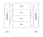
図16は、第1の実施の形態のメモリセルアレイ構成の場合に、ロウデコーダのなかのメモリセルユニットMU0に対するワード線駆動回路DRV0と、メモリセルユニットMU1に対するワード線駆動回路DRV1とを、メモリセルアレイのワード線方向の両端部に振り分けて配置した第5の実施の形態の構成を示す図である。メモリセルユニット数が4個以上と多い場合には、同様の手法で、隣接する二つのメモリセルユニットでそれらのワード線駆動回路を左右に振り分けるようにして、メモリセルアレイの両側にワード線駆動回路を配置する。
【0082】
NANDセルブロック毎にワード線駆動回路を左右に振り分ける手法は、既に特願平6−198840号明細書(平成6年8月23日出願)や、米国特許第5,517,457号明細書、米国特許第5,615,163号明細書等に開示されている。この発明では、NANDストリング内をメモリセルユニットとしてブロック化しているから、そのブロック毎に、図示のようにワード線駆動回路を振り分けて配置することにより、NANDストリング毎にワード線駆動回路を振り分けた場合に比べて、レイアウト上のフレキシビリティがより向上し、コンパクトな設計が可能となる。特にデザイン・ルールが小さくなり、一つのメモリセルユニットの幅内にワード線駆動回路の高耐圧トランジスタを配置できない場合に、有効である。
【0083】
第6の実施の形態
図17は更に、メモリセルユニットの2個ずつについて、ワード線駆動回路DRV0,DRV1を左右に振り分け配置した第6の実施の形態の構成を示す図である。図16に示す第5の実施の形態の場合に比べて更にデザイン・ルールが小さくなり、二つのメモリセルユニットの範囲内に高耐圧トランジスタを配置できない場合には、この様なワード線駆動回路の配置とすればよい。
【0084】
本発明の更に他の実施の形態を説明する前に、図15に示す第4の実施の形態において、ブロック分離選択トランジスタST0〜ST6をメモリセルMC0〜MC7と同様な構造にした場合の例を考え、そのレイアウトを図20に示し、この図20のA−A′断面を図21に示す。
【0085】
この場合のメモリセルサイズのブロック分離選択トランジスタ間のメモリセル数依存性を図22に示す。ここでFはFeature size、すなわちデザイン・ルールを示してい。また、この例においては、メモリサイズは1つのメモリセルユニットが16個のメモリセルで構成されている場合を示している。
【0086】
この例においては、ブロック分離選択トランジスタを利用して、ブロック分割することにより、従来のNANDセルのストリングにおいて、選択トランジスタ間のメモリセル数を少なくしていく場合に比べて、はるかに小さな面積のメモリセルが実現できる。例えば、選択トランジスタ若しくはブロック分離選択トランジスタ間のメモリセル数を1個の場合、従来のNANDセルのストリングの約半分のセルサイズが実現できる。
【0087】
しかし、選択トランジスタ間のメモリセル数が16個の場合のセルサイズを100とすると、ブロック分離選択トランジスタ間のメモリセル数が1個となると、セルサイズが219と約2倍に増大してしまう(図22参照)。
【0088】
図23(a),(b),(c)を用いてこの理由を説明する。従来型でしかも選択トランジスタ間のメモリセル数が多い場合、メモリセル1個のサイズは素子分離にSTI(Shallow Trench Isolation)を用いると、ビット線ピッチ2F×ワード線ピッチ2F=4F2 のセルサイズがほぼ実現できる(図23(a)参照)。しかし、本発明のNANDストリングはビット線ピッチ2F×ワード線ピッチ4F=8F2 にほぼ等しくなってしまう(図23(b)参照)。これは、図23(c)で示しAND型EEPROMのビット線ピッチ4F×ワード線ピッチ2F=8F2 とほぼ同じメモリサイズとなる。なおこのAND型EEPROMの断面図を図24に示す。
【0089】
そこで、ブロック分離選択トランジスタ間のメモリセル数を減らしてもメモリセルサイズが増加しない例を本発明の第7および第8実施の形態として以下に説明する。
【0090】
第7の実施の形態
この第7の実施の形態のNAND型EEPROMは、図11に示す第2の実施の形態のNAND型EEPROMにおいて、読み出し、消去、書き込みを図25、図26、図27に示すように制御するようにした構成となっている。読み出し、書き込みに関しては、ワード線WL19が選択された場合を考える。基本的な特徴は、常にブロック分離選択トランジスタのゲート電圧はそれぞれの場合、等しい電圧に制御することである。
【0091】
すなわち、読み出し時は、選択ゲート線STL0,STL1,STL2は全て、電圧Vreadにする(図25参照)。
【0092】
また、消去時は選択ゲート線STL0,STL1,STL2は全てα×Veraフローティングにする(図25)。さらに、書き込み時は選択ゲート線STL0,STL1,STL2は全て電圧Vreadとし、選択ゲート線GSLをVssとする。選択ゲート線STL2がVreadでも、非選択ブロックのワード線WL24〜WL31がVreadとなるため、書き込み禁止のNANDストリング内のブロック分離選択トランジスタST2はカットオフする。
【0093】
したがって、この第7の実施の形態のNAND型EEPROMは、図28に示すように、ブロック分離選択ゲート線STLを共通にできる。
【0094】
第8の実施の形態
本発明の第8の実施の形態は、図15に示す第4の実施の形態において、読み出し、消去、書き込みの電圧条件を図29、図30、図31に示すように構成したものである。読み出し、書き込みに関しては、ワード線WL3が選択された場合を示している。
【0095】
したがって、第7の実施と同様に、この第8の実施の形態の構成も図32に示すようにブロック分離選択ゲート線STLを共通にできる。また、ビット線側の選択ゲートSSLも共通にした場合、第7の実施の形態、第8の実施の形態は各々図33、図34に示すように構成しても有効である。ただし、セルソース線側の選択ゲートGSLは、書き込み時にVssにする必要があり、これは、共通化できない。
【0096】
なお第7および第8の実施の形態においては、ブロック分選択ゲート線を全て共通にしたが、少なくとも2つのブロック分離選択ゲート線を共通に接続しても良い。
【0097】
次に本発明のNAND型EEPROMの製造方法およびプロセスの構成を説明する。ブースタプレート技術が最近提案されているが、これと同様なプロセスを本発明の製造方法に利用すれば良い。
【0098】
まず、提案されたブースタプレートなる導電体を用いて非書き込みNAND列のチャネル電位を高くし、かつ、書き込み/消去/読み出しの電圧を低下させるNAND型EEPROMについて説明する。
【0099】
このNAND型EEPROMについては文献(J.D.Choi et al., "A Novel Booster Plate Technology in High Density NAND Flash Memories for Voltage Scaling-Down and Zero Program Disturbance," in Symp. VLSI Technology Dig. Tech. Papers, June 1996, pp.238-239)に記載されている。
【0100】
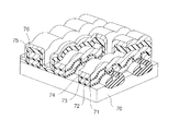
図35は、ブースタプレートを有するNAND型EEPROMの構成を示す斜視図であり、このNAND型EEPROMは次のように構成されている。図35に示すように、基板70はゲート絶縁膜71を介して浮遊ゲート72が形成され、この浮遊ゲート72上にONO膜73を介して制御ゲート74が形成されている。そして、さらに前記制御ゲート74上にはプレート酸化膜75を介してブースタプレート76が形成されている。
【0101】
すなわち、上記文献のNAND型EEPROMは、従来のNAND型EEPROMを作製した後に、プレート酸化膜75であるCVD酸化膜(SiO2 )とタングステン・ポリサイド(poly−SiとWSiX )を堆積し、その後、ポリサイド層をパターニングし、各ブロックの全メモリセル・トランジスタを覆うブースタプレート76を形成したものである。
【0102】
メモリセルの動作は、基本的には従来のNAND型EEPROMとほぼ同様であるが、ブースタプレート76には、書き込み時に書き込み電圧が、また消去時に0Vがそれぞれ印加される。
【0103】
ところで、前記ブースタプレートには2つの利点がある。一つは、書き込みの際の容量カップリングγが大きくなることである。ブースタプレートがない従来のNAND型EEPROMにおいて、容量カップリングγは、
γ=Ccf/(Cfs+Ccf)
と表わされる。ここで、Ccfは制御ゲート(ワード線)74と浮遊ゲート72間の容量であり、Cfsは浮遊ゲート72と基板70間の容量である。一方、ブースタプレート76を付加した場合の容量カップリング比γbは、
γb=(Ccf+Cbf)/(Cfs+Ccf+Cbf)
と表わされ、従来のブースタプレートがない場合のγよりも大きくなる。したがって、書き込み時の書き込み電圧を低下できる。ここで、Cbfはブースタプレート76と浮遊ゲート72間の容量である。
【0104】
また、消去時の容量カップリング比は、(1−γb)で表わされるため、基板70と浮遊ゲート72間の電位差を大きくでき、従来よりも高速な消去、あるいは、消去電圧を低下することが可能となる。また、γbが大きくなることによって、読み出し時におけるパス・トランジスタへの印加電圧も低下できる。
【0105】
もう一つの利点は、制御ゲート(ワード線)74とチャネル間の容量カップリング比が大きくなることである。ブースタプレート76がある場合の容量カップリング比Bbは、
Bb=(Cox+Cboot)/(Cox+Cboot+Cj)
と表わされる。ここで、Coxは制御ゲート(ワード線)74とチャネルとの間のゲート容量の総和、Cbootはブースタプレート76とチャネルとの間のゲート容量の総和、Cjはセルトランジスタのソースおよびドレインの接合容量の総和である。したがって、書き込み時にパス・トランジスタの電圧を過度に高めなくても、書き込み禁止のNAND列のチャネル電位を高くすることができ、誤書き込みに対するマージンが向上できる。
【0106】
このブースタプレートをブロック分離選択ゲート線に利用すれば良い。
【0107】
次に本発明のNAND型EEPROMの製造方法について説明する。図36〜図50は、本発明のNAND型EEPROMの製造工程を示す図である。図36,39,42,45,48は、本発明のNAND型EEPROMの製造工程における平面図であり、図37,40,43,46,49はそれぞれの製造工程における平面図中のX−X′に沿った断面図、図38,41,44,47,50はそれぞれの製造工程における平面図中のY−Y′に沿った断面図である。
【0108】
図36〜図38に示すように、p形シリコン基板81上にメモリセルnウェル82を形成し、このメモリセルnウェル82内にメモリセルpウェル83を形成する。このメモリセルpウェル83上に、フィールド酸化膜(素子分離絶縁膜)84を形成する。以下に上記フィールド酸化膜84で囲まれた領域への、NANDセル、ここでは4個のメモリセルトランジスタとそれを挟む2つの選択ゲートトランジスタからなるNANDセルの製造方法を示していく。
【0109】
前記メモリセルpウェル83上にフィールド酸化膜84を形成後、図39〜図41に示すように、膜厚が5nm〜20nmの熱酸化膜からなる第1のゲート絶縁膜85を成膜する。さらに、この第1のゲート絶縁膜85上に、膜厚が1000nm以上の第1の多結晶シリコン膜あるいはシリサイド膜と多結晶シリコン膜との積層膜あるいは金属膜からなるブースタプレート86を成膜する。
【0110】
続いて、図40に示すように、マスク材とするシリコン窒化膜(SiN)87をリソグラフィ法により形成し、さらにこのシリコン窒化膜87の側面に側壁88を形成する。そして、このシリコン窒化膜87および側壁88をマスクとして、図43に示すように、前記第1のゲート絶縁膜85およびブースタプレート86を制御ゲート線方向に沿った線状にエッチング加工する。
【0111】
次に、図42〜図44に示すように、膜厚が5nm〜10nmの熱酸化膜からなる第2のゲート絶縁膜89を成膜する。この第2のゲート絶縁膜89上に、膜厚が1000nm以上の第2の多結晶シリコン膜あるいはシリサイド膜と多結晶シリコン膜との積層膜あるいは金属膜からなる浮遊ゲート90を成膜する。さらに、図44に示すように、制御ゲート線方向の隣接するフィールド酸化膜84上で浮遊ゲート90間の分離溝91を形成する。
【0112】
その後、前記浮遊ゲート90上に、膜厚が15nm〜40nmの第3のゲート絶縁膜92を形成する。さらに、この第3のゲート絶縁膜92上に、膜厚が100nm〜400nmの第3の多結晶シリコンあるいはシリサイド膜と多結晶シリコン膜との積層体あるいは金属からなる膜93を堆積する。
【0113】
次に、図45〜図47に示すように、上記膜93と浮遊ゲート90を、互いに隣接するブースタプレート86間及びブースタプレート86の上面の一部上で残存するように、セルフアラインでエッチング加工する。これにより、ワード線(制御ゲート)93、選択ゲート線93a及び浮遊ゲート90を形成する。
【0114】
その後、NANDセルのドレイン部とソース部に、イオン注入によりN+ 層184を、セルフアラインで形成する。この際、NANDセルのメモリセルトランジスタ間のドレイン/ソース領域はブースタプレート86で覆われているため、N+ 層が形成されない。
【0115】
次に、図48〜図50に示すように、第4の絶縁膜95を全面に堆積し、この第4の絶縁膜95にコンタクト孔96を開ける。さらに、このコンタクト孔96にタングステンプラグ97を埋め込み、このタングステンプラグ97に接続されるアルミニウム(Al)からなるビット線98を配設する。そして、パシベーション膜99で全面を覆う。以上により、本発明のNAND型EEPROMは完成する。最後に、図46、図48のA,B,Cで示したブロック分離選択ゲート線をメモリアレイ端、若しくは、サブアレイ端で電気的に共通になるように、その他の配線若しくは、同一の配線で結線する。
【0116】
【発明の効果】
以上のようにこの発明によれば、1つのNANDセルブロック内に複数の消去ブロックを設定することが可能であり、消去ブロックサイズを増やすことなく、1つのNANDストリング内のメモリセルの個数を増やすことを可能としたNAND型EEPROMが得られる。
【図面の簡単な説明】
【図1】この発明の第1の実施の形態によるNAND型EEPROMのメモリセルアレイの等価回路。
【図2】第1の実施の形態にかかるメモリセルアレイのレイアウト。
【図3】図2に示す切断線A−A′に沿った断面図。
【図4】図2に示す切断線B−B′に沿った断面図。
【図5】第1の実施の形態のNAND型EEPROMのブロック構成を示す図。
【図6】第1の実施の形態のNAND型EEPROMのセンスアンプ構成を示す図。
【図7】第1の実施の形態のNAND型EEPROMのデータ消去動作のバイアス関係を示す図。
【図8】第1の実施の形態のNAND型EEPROMのデータ書き込み動作のバイアス関係を示す図。
【図9】図8のバイアス関係をメモリセルアレイ上で示す図。
【図10】第1の実施の形態のNAND型EEPROMのデータ読み出し動作のバイアス関係を示す図。
【図11】第2の実施の形態にかかるメモリセルアレイの構成を示す図。
【図12】第2の実施の形態でのデータ消去動作のバイアス関係を示す図。
【図13】第2の実施の形態でのデータ書き込み動作のバイアス関係を示す図。
【図14】第3の実施の形態にかかるメモリセルアレイの構成を示す図。
【図15】第4の実施の形態にかかるメモリセルアレイの構成を示す図。
【図16】第5の実施の形態にかかるワード線駆動回路の配置を示す図。
【図17】第6の実施の形態にかかるワード線駆動回路の配置を示す図。
【図18】従来のNAND型EEPROMのメモリセルアレイ構成を示す図。
【図19】従来のNAND型EEPROMのデータ消去、読み出し及び書き込みのバイアス関係を示す図。
【図20】第4の実施の形態によるメモリセルアレイのレイアウト図。
【図21】第4の実施の形態によるメモリセルアレイの断面図。
【図22】選択トランジス間のメモリセル数とセルサイズとの関係を示すグラフ。
【図23】各メモリセルのサイズを説明する図。
【図24】AND型EEPROMの断面図。
【図25】第7の実施の形態のデータ読出し動作のバイアス関係を示す図。
【図26】第7の実施の形態のデータ消去動作のバイアス関係を示す図。
【図27】第7の実施の形態のデータ書込み動作のバイアス関係を示す図。
【図28】第7の実施の形態にかかるメモリセルアレイの構成を示す図。
【図29】第8の実施の形態のデータ読出し動作のバイアス関係を示す図。
【図30】第8の実施の形態のデータ消去動作のバイアス関係を示す図。
【図31】第8の実施の形態のデータ書込み動作のバイアス関係を示す図。
【図32】第8の実施の形態にかかるメモリセルアレイの構成を示す図。
【図33】第7の実施の形態の変形例にかかるメモリセルアレイの構成を示す図。
【図34】第8の実施の形態の変形例にかかるメモリセルアレイの構成を示す図。
【図35】ブースタプレートを有するNAND型EEPROMの構成を示す斜視図。
【図36】本発明によるNAND型EEPROMの製造工程における平面図。
【図37】図36に示す切断線X−X’に沿った断面図。
【図38】図36に示す切断線Y−Y’に沿った断面図。
【図39】本発明によるNAND型EEPROMの製造工程における平面図。
【図40】図39に示す切断線X−X’に沿った断面図。
【図41】図39に示す切断線Y−Y’に沿った断面図。
【図42】本発明によるNAND型EEPROMの製造工程における平面図。
【図43】図42に示す切断線X−X’に沿った断面図。
【図44】図42に示す切断線Y−Y’に沿った断面図。
【図45】本発明によるNAND型EEPROMの製造工程における平面図。
【図46】図45に示す切断線X−X’に沿った断面図。
【図47】図45に示す切断線Y−Y’に沿った断面図。
【図48】本発明によるNAND型EEPROMの製造工程における平面図。
【図49】図48に示す切断線X−X’に沿った断面図。
【図50】図48に示す切断線Y−Y’に沿った断面図。
【符号の説明】
1 NANDセルブロック
MC メモリセルトランジスタ
SST,GST 選択トランジスタ
ST ブロック分離選択トランジスタ
WL ワード線
BL ビット線
SL ソース線
SSL,GSL,STL 選択ゲート線
MU0〜MU3 メモリセルユニット
51 メモリセルアレイ
52 ロウデコーダ
53 センスアンプ回路
54 カラムデコーダ
55 カラムゲート
56 昇圧回路
57 制御回路
DRV0,DRV1 ワード線駆動回路[0001]
BACKGROUND OF THE INVENTION
The present invention relates to a nonvolatile semiconductor memory device (EEPROM) in which a plurality of electrically rewritable memory cells are connected in series to constitute a NAND cell (memory cell string).
[0002]
[Prior art]
Conventionally, a NAND cell type EEPROM is known as an EEPROM that can be electrically rewritten. One memory cell of a NAND cell type EEPROM has a transistor having a stack structure in which a floating gate (charge storage layer) and a control gate are stacked on a semiconductor substrate via an insulating film. A plurality of memory cells are connected in series so that adjacent ones share a source / drain to form a NAND cell. Such NAND cells are arranged in a matrix to form a memory cell array.
[0003]
The drains on one end side of the NAND cells arranged in the column direction of the memory cell array are commonly connected to the bit line via the selection transistor, and the source on the other end side is also connected to the common source line via the selection transistor. The word line of the memory cell transistor and the gate electrode of the selection transistor are commonly connected as a word line (control gate line) and a selection gate line in the row direction of the memory cell array, respectively.
[0004]
Such a NAND cell type EEPROM is known, for example, from the following documents (1) and (2).
[0005]
▲ 1 ▼ K. -D. Suh et al., "A 3.3V 32Mb NAND Flash Memory with Incremental Step Pulse Programming Scheme," IEEE J. Solid-State Circuits, Vol.30, pp.1149-1156, Nov.1995
(2) Y. Iwata et al., "A 35ns Cycle Time 3.3V Only 32Mb NAND Flash EEPROM," IEEE J. Solid-State Circuits, Vol.30, pp.1157-1164, Nov.1995.
FIG. 18 shows a configuration of one NAND cell block of the memory cell array of the NAND cell type EEPROM. The plurality of memory cells M are connected in series in such a manner that their sources and drains are shared by adjacent ones to form a NAND cell. One end of the NAND cell is connected to the bit line BL via the selection transistor S1, and the other end is also connected to the common ground line via the selection transistor S2. The control gates of the memory cells M arranged in the horizontal direction in FIG. 18 are commonly connected to the word line WL. Similarly, the gates of the selection transistors S1 and S2 are commonly connected to the selection gate lines SSL and GSL. A range of NAND cells driven by one word line constitutes a NAND cell block.
[0006]
Usually, a plurality of such NAND cell blocks are arranged in the bit line direction to constitute a memory cell array. Each NAND cell block is a unit of data erasing and so-called batch erasing is performed. A memory cell column along one selected word line in the NAND cell block is called one page, and one page is a unit for data reading and writing.
[0007]
In the memory cell M, for example, in the case of an n channel, the threshold value in which electrons are injected into the floating gate is positive (E type state), and the threshold value in which electrons are emitted from the floating gate is negative (D The data is stored by associating the “type state” with the binary value. For example, the D type state is defined as “1” data holding state (erasing state), and the E type state is defined as “0” data holding state (writing state). The operation of shifting the threshold value of the memory cell holding “1” data in the positive direction to shift to the state of holding “0” data is “write operation”, and holds “0” data. An operation of shifting the threshold value of the memory cell in the negative direction to shift to a state in which “1” data is held is defined as an “erase operation”. In this specification, the following description is made according to this definition.
[0008]
FIG. 19 shows the potential relationship between the data erasing, reading and writing operations in the selected NAND cell block of the memory cell array. In the erase operation, all the word lines of the selected NAND cell block are set to 0 V, the select gate lines SSL and GSL and the bit line BL are set to the floating (F), and a high positive erase voltage Vera (for example, the P-type well of the memory cell) 3 ms, 21 V erase pulse). As a result, in the selected block, an erasing voltage is applied between the well and the word line, and electrons in the floating gate are discharged to the well by an FN (Fowler-Nordheim) tunnel current. As a result, the memory cells in the NAND cell block are in the erased state of “1”.
[0009]
At this time, the unselected NAND cell block is not affected by the erase pulse due to capacitive coupling between the word line and the well in the floating state. The coupling ratio is calculated from the capacitance connected to the floating word line. Actually, the capacitance between the polysilicon word line and the P well in the cell region is dominant with respect to the total capacitance, and the coupling ratio obtained from the actual measurement result is as large as about 0.9. Block the flow. Erase verification (verification) is determined based on whether or not the threshold voltage of all the memory cells in the selected block is, for example, −1 V or less.
[0010]
In the data reading operation, 0 V is applied to the selected word line, and a constant read voltage Vread (voltage necessary for conducting the channel regardless of the threshold) is applied to the unselected word line and the selected gate line, and the selected memory cell is selected. This is done by reading the potential change of the bit line BL according to the presence or absence of conduction.
[0011]
In the data write operation, a positive high write voltage Vpgm is applied to the selected word line, a pass voltage Vpass is applied to the unselected word line, Vcc is applied to the select gate line SSL on the bit line side, and Vss = 0 V is applied to the select gate line GSL on the common source line side. And Vss is applied to the bit line BL to which “0” is to be written, and Vcc is applied to the bit line BL to which writing is inhibited (that is, to be kept in the erased state of “1”). At this time, in the selected memory cell connected to the bit line to which Vss is applied, the channel potential is held at Vss, a large electric field is applied between the control gate and the channel, and electron injection due to a tunnel current occurs from the channel to the floating gate. In other non-selected memory cells to which Vpass connected to the same bit line is applied, a sufficient electric field is not applied to writing, and writing is not performed.
[0012]
In the memory cell along the bit line to which Vcc is applied, the channel of the NAND cell is precharged to Vcc or Vcc-Vth (Vth is the threshold voltage of the selection transistor), and the selection transistor is cut off. When the write voltage Vpgm and the pass voltage Vpass are applied to the control gate, the channel potential increases due to capacitive coupling between the channel of the floating NAND cell and the control gate to which Vpgm or Vpass is applied. Does not happen.
[0013]
As described above, electron injection is performed and "0" is written only in the memory cell at the intersection of the bit line to which Vss is applied and the selected word line to which Vpgm is applied. In the write-inhibited memory cell in the selected block, the channel potential is determined by the capacitive coupling between the word line and the channel as described above. Therefore, in order to make the write-inhibit potential sufficiently high, the channel is initially charged. It is important to sufficiently carry out and increase the capacitance coupling ratio between the word line and the channel.
[0014]
The coupling ratio B between the word line and the channel is calculated by B = Cox / (Cox + Cj). Here, Cox is the total gate capacitance between the word line and the channel, and Cj is the total junction capacitance of the source and drain of the memory cell transistor. The channel capacity of the NAND cell is the sum of the total sum Cox of these gate capacities and the total sum Cj of junction capacitances. Further, other capacities such as an overlap capacity between the selection gate line and the source and a capacity between the bit line, the source and the drain are very small as compared with the total channel capacity, and are ignored here.
[0015]
[Problems to be solved by the invention]
In the NAND type EEPROM described above, scaling in the plane direction (design rule) has been performed conventionally, but scaling in the depth direction (oxide film thickness) corresponding to this has not been performed. Specifically, the thickness of the tunnel oxide film is almost constant at 10 nm in 16M, 32M, 64M, 256M bit NAND type EEPROM. If the thickness of the tunnel oxide film is constant, in order to make the electric field applied to the tunnel oxide film constant, the rewrite voltage of the memory cell must also be maintained at a constant voltage and cannot be lowered. Although attempts have been made to further reduce the thickness of the tunnel oxide film by a process engineer, for example, a 5 nm oxide film has not been realized. In order to reduce the rewrite voltage, the capacitance between the control gate and the floating gate may be increased to increase the coupling ratio. However, this also requires a device such as a thin oxide film between the control gate and the floating gate or an increase in the capacitor area between the control gate and the floating gate, which cannot be easily achieved.
[0016]
In the end, NAND-type EEPROM requires a high voltage of about 20 V as a rewrite voltage from 16 M to 256 Mbit. For this reason, the transistor of the row decoder that drives the high voltage to the word line must be designed with a high breakdown voltage transistor. The high withstand voltage transistor has been devised to weaken the applied electric field by loosening the design rule and increasing the size of each part in the transistor, as compared with the normal transistor of the peripheral circuit. For example, in the case of a 256 Mbit NAND type EEPROM designed with a 0.25 μm rule, the high breakdown voltage transistor has a design rule several times larger than that of a normal transistor in a peripheral circuit. The pitch (length) of one NAND string composed of 16 memory cells of 256 Mbit NAND EEPROM and two selection transistors is 8.5 μm, and two or more high voltage transistors are included in the pitch. It cannot be arranged, and the arrangement of one high voltage transistor is the limit.
[0017]
For example, in the
[0018]
However, simply increasing the number of memory cell transistors in one NAND string simultaneously increases the erase block size. This is because in the conventional NAND type EEPROM, the NAND string (NAND cell) is one block, and only erasing in units of blocks is allowed. The reason that only erasing in the NAND cell block unit is allowed is as follows. For example, it is assumed that a NAND string composed of 16 memory cells has eight memory cells as one block as a unit of rewriting, and the lower block is selected and rewritten many times. Then, a stress of the pass voltage Vpass is applied to the word line of the upper block, and the threshold voltage of the non-selected block also changes when rewriting is performed many times.
[0019]
The size of this erase block is gradually increased with the increase in capacity to 4 Kbytes for 16 Mbit NAND type EEPROM, 8 Kbytes for 32 Mbit NAND type EEPROM, and 16 Kbytes for 256 Mbit NAND type EEPROM. . However, for example, when a NAND type EEPROM is used as a film medium of a digital camera, there is a demand that a sudden increase in block size is not desired in order to maintain compatibility. Therefore, even in a large-
[0020]
The present invention has been made in view of the above circumstances, and an object thereof is to provide a NAND type EEPROM in which a plurality of erase units can be set in one NAND cell block.
[0021]
[Means for Solving the Problems]
A first aspect of a nonvolatile semiconductor memory device according to the present invention includes a first signal line, a second signal line, and an electrically rewritable memory between the first signal line and the second signal line. A NAND cell configured by connecting a plurality of cells in series, and a block isolation selection transistor interposed between predetermined adjacent memory cells in the NAND cell in order to divide the NAND cell into a plurality of blocks. It is characterized by.
[0022]
In the present invention, the gates of at least two or more block separation selection transistors between a plurality of blocks may be connected in common.
[0023]
According to a second aspect of the nonvolatile semiconductor memory device of the present invention, an electrically rewritable memory cell selected by a word line has a selection transistor interposed between the first signal line and the second signal line, respectively. Are connected in series to form a NAND cell, a memory cell array in which a plurality of NAND cells are arranged, an address decoder that selects a memory cell of the memory cell array by an address, and senses data read from the memory cell array A sense amplifier circuit having a function of latching write data to the memory cell array, and a control circuit for controlling writing, erasing and reading of data to the memory cell array. Block isolation selection transistor interposed between predetermined adjacent memory cells Characterized in that it is divided into a plurality of memory cell units by register.
[0024]
In the present invention, specifically, at the time of data rewriting of the memory cell array, one of the plurality of memory cell units is selected as an erasing unit, and data erasing is performed, and a plurality of data along one word line is selected. Data is written with a predetermined range of memory cells as one page.
[0025]
In the present invention, the data erasing is performed by applying a ground potential to all the word lines of the selected memory cell unit, and all the word lines of the non-selected memory cell units, the first signal line side and the second signal line side. The selection gate lines connected to the gates of the selection transistor and the block isolation selection transistor are set in a floating state, and an erase voltage is applied to the substrate region on which the memory cell array is formed.
[0026]
In the present invention, the data write is performed by applying a ground potential and a power supply potential to the first signal line in accordance with the data “0” and “1” to be written, and storing the memory on the non-selected word line in the selected memory cell unit. A selection gate line that applies a pass voltage for conducting the cell and connects to all word lines of the non-selected memory cell unit and a gate of the block isolation selection transistor between the non-selected memory cell unit and the selected memory cell unit Is applied by applying a read voltage lower than the pass voltage for conducting the memory cell, and applying a write voltage higher than the pass voltage to the selected word line of the selected memory cell unit.
[0027]
In the present invention, more specifically, the memory cell array is interposed between predetermined adjacent memory cells in each NAND cell. n −1 (n: positive integer) block separation selection transistors, 2 n Divided into memory cell units. In this case, each memory cell unit may include the same number of memory cells, or may include a different number of memory cells.
[0028]
In the present invention, it is preferable that the word line driving circuit in the address decoder is arranged at both ends in the word line direction of the memory cell array in units of one or two memory cell units.
[0029]
According to a third aspect of the nonvolatile semiconductor memory device of the present invention, a plurality of electrically rewritable memory cells selected by different word lines are connected in series to a bit line to form a NAND cell, and the word line A plurality of NAND cells arranged in a direction constitute a NAND cell block, and the NAND cell block is divided into a plurality of memory cell units by a block separation selection transistor interposed between predetermined adjacent memory cells of each NAND cell. A memory cell array; an address decoder that selects a memory cell of the memory cell array by an address; a sense amplifier circuit having a function of sensing read data from the memory cell array and latching write data to the memory cell array; One of the memory cell units Data rewriting means for selecting data as a last unit and erasing data in the memory cell unit at once, and writing data with a predetermined range of a plurality of memory cells along one word line as one page. It is characterized by.
[0030]
According to the present invention, a plurality of erase blocks can be set in one NAND cell block by interposing a block separation selection transistor in the NAND cell, and the memory in one NAND string can be set without increasing the erase block size. It becomes possible to increase the number of cells.
[0031]
According to a fourth aspect of the nonvolatile semiconductor memory device of the present invention, the first and second signal lines, the first and second select transistors, each include a plurality of electrically rewritable memory cells. 1st to n-th (n ≦ 3) NAND cell blocks configured in series, and first to (n−1) -th block isolation selection transistors, and the first signal line includes The first selection transistor is connected, the first NAND cell block is connected to the first selection transistor, and the i-th block separation selection is connected to the i-th (1 ≦ i ≦ n−1) NAND cell block. The transistor is connected, the (i + 1) th NAND cell block is connected to the ith (1 ≦ i ≦ n−1) block isolation selection transistor, and the second selected transistor is connected to the nth NAND cell block. Are connected, the second signal line is connected to the second selection transistor, and the gates of at least two of the first to nth block isolation selection transistors are commonly connected. Features.
[0032]
According to a fifth aspect of the nonvolatile semiconductor memory device of the present invention, the first and second signal lines, the first and second selection transistors, and the first to nth rewritable elements are electrically rewritable. A memory cell; and first to (n-1) th block separation selection transistors, wherein the first selection transistor is connected to the first signal line, and the first selection transistor is connected to the first selection transistor. Are connected to the i-th (1 ≦ i ≦ n−1) memory cell, and the i-th (1 ≦ i ≦ n−1) block separation selection transistor is connected to the i-th (1 ≦ i ≦ n−1) memory cell. The (i + 1) th memory cell is connected, a second selection transistor is connected to the nth memory cell, a second signal line is connected to the second selection transistor, and the first to nth block isolations Selection transition Of data, characterized in that the gate of the at least two blocks separating selection transistors are commonly connected.
[0033]
In the fourth and fifth embodiments, the gates of the first and second selection transistors are made of polycrystalline silicon, a stacked body of polycrystalline silicon and silicide, or a metal electrode, and the first to second ( The gate of the n-1) block separation selection transistor may be composed of polycrystalline silicon, a stacked body of polycrystalline silicon and silicide, or a metal electrode.
[0034]
In the fourth and fifth embodiments, the gates of the first and second selection transistors are made of polycrystalline silicon, a stacked body of polycrystalline silicon and silicide, or a metal electrode, and the first to second transistors The gate of the (n-1) -th block separation selection transistor may be constituted by polycrystalline silicon, a stacked body of polycrystalline silicon and silicide, or a metal electrode.
[0035]
At the time of data writing, a power supply voltage Vcc or a read voltage Vread higher than that is applied to the gates of the first selection transistor and the first to (n-1) th block separation selection transistors, and the second A ground voltage Vss may be applied to the gate of the selection transistor.
[0036]
Note that the first signal line is preferably a bit line and the second signal line is preferably a cell source line.
[0037]
The memory cell is preferably an electrically rewritable memory cell having a two-layer stack structure having a floating gate and a control gate formed on the floating gate via an insulating film.
[0038]
DETAILED DESCRIPTION OF THE INVENTION
First embodiment
FIG. 1 shows an equivalent circuit of a memory cell array of one
[0039]
In this embodiment, in addition to the above-described two selection transistors SST and GST, a selection transistor ST for block separation is provided by dividing one NAND cell into two. That is, the
[0040]
FIG. 2 shows a layout of the
[0041]
The
[0042]
The overall block configuration of a NAND-type EEPROM having a page write / read function is as shown in FIG. As shown in the figure, a
[0043]
The
[0044]
The
[0045]
The
[0046]
FIG. 6 shows the configuration of one sense amplifier in the
[0047]
The other node Q of the
[0048]
Next, data erase, write, and read operations of the NAND type EEPROM according to this embodiment will be described in order.
[0049]
FIG. 7 shows the bias potential relationship of each part in the data erasing operation. As described above, in the conventional NAND type EEPROM, one NAND cell block is an erasing unit, whereas in this embodiment, the memory units MU0 and MU1 shown in FIG. 1 are erasing units. FIG. 7 shows an example of a data erasing operation in which the lower memory unit MU1 is a selected block and the upper memory unit MU0 is a non-selected block.
[0050]
That is, in FIG. 1, the range of word lines WL0 to WL15 is a non-selected block, and the range of WL16 to WL31 is a selected block. When the erase operation is started, Vss (0 V) is applied to the word lines WL16 to WL31 of the selected block to be erased, and the word lines WL0 to WL15 and the selection gate lines SSL, GSL, and STL of the unselected block are in a floating state. To be. In this state, the erase voltage Vera (20 V) is applied to the p-well of the memory cell array.
[0051]
At this time, the word lines WL0 to WL15 and the selection gate lines SSL, STL, and GSL of the non-selected block are boosted to α × Vera by capacitive coupling with the p-well. Since α is about 0.9, it rises to about 18V. The bit lines BL0 and BL1 and the source line SL are connected to the p well and the bit line contact portion n. + N of the diffusion layer and the source line SL portion + The PN junction with the mold diffusion layer is in a forward bias state and rises to Vera-Vf. Since Vf is a built-in potential of the PN junction and is about 0.7V, the bit lines BL0 and BL1 and the source line SL are about 19.3V. Therefore, the erase operation does not occur in the memory cell transistors along the word lines WL0 to WL15 of the non-selected block.
[0052]
In the memory cell transistors along the word lines WL16 to WL31 in the selected block, Vera is applied to the substrate region and Vss is applied to the control gate. Therefore, electrons in the floating gate are emitted to the substrate region (p well) by tunnel current. The data stored in the memory cell transistors is erased at once.
[0053]
FIG. 8 shows the bias potential relationship of each part in the data write operation. FIG. 8 shows a case where writing is performed on the word line WL17 in the selected block (that is, the memory unit MU1) erased collectively in the above description. Further, it is assumed that “0” data is written on the bit line BL0 and “1” data is written on the bit line BL1 (that is, write prohibition that keeps the erased state of “1” data).
[0054]
In this case, FIG. 9 shows the potential relationship by extracting only two bit lines BL0 and BL1 from the bit lines shown in FIG.
[0055]
In this data write, first, the write ground potential Vss and the write inhibit power supply potential Vcc are respectively applied to the bit lines BL0 and BL1. Thereafter, while the selection gate line GSL on the source line side is kept at Vss, a read voltage Vread (about 3.5 V) slightly higher than Vcc is applied to the other word lines and selection gate lines. As a result, the potential Vss for writing is transmitted to the NAND cell channel connected to the bit line BL0. Vcc for write inhibition is transmitted to the NAND cell channel connected to the bit line BL1, but the channel potential is Vread−Vth (the threshold voltage that is higher than the threshold voltage of the selection transistor or the memory cell transistor). When the voltage rises to a value lowered by (value voltage), the select transistor SST is turned off and the channel is floated.
[0056]
In this state, among the word lines of the selected block, the non-selected word lines WL16 and WL18 to WL31 that are not to be written have a pass voltage Vpass (about 8V) higher than the read voltage Vread, which is the selected word line to which the write is to be performed. A higher write voltage Vpgm (about 16 V) is applied to WL17. The word lines WL0 to WL15, the drain side selection gate line SSL, and the block separation selection gate line STL in the unselected block keep the potential at the value Vread.
[0057]
At this time, the channel region on the bit line BL1 side in the selected block has β × (Vpass−Vread) + (Vcc−Vth) due to capacitive coupling with the word rising from the initial potential Vcc−Vth to the potentials Vpass and Vpgm. ). Since the number of word lines to which the potential Vpass is applied is 15 for one word line to which the potential Vpgm is applied, the above-described channel potential determined by the value Vpass is obtained. Here, β is a capacitance coupling ratio between the word line and the channel region, and is about 0.5.
[0058]
At this time, the block isolation select transistor ST1 on the write-inhibited bit line BL1 side has a gate voltage of Vread, and as a result of the channel voltage being boosted as described above, the gate-source voltage becomes negative and cut off. That is, on the write-inhibited bit line BL1 side, the channel region in the selected block including the memory cell transistor MC171 is boosted in a floating state separated from the channel region on the memory cell unit MU0 side which is a non-selected block.
[0059]
On the other hand, on the bit line BL0 side to which the potential Vss is applied, the block isolation selection transistor ST0 is kept on by the potential Vss transmitted from the bit line BL0. Therefore, the potential Vss is transmitted to the channel of the selected memory cell transistor MC170. As a result, in the memory cell transistor MC170 driven by the selected word line WL17 to which the write voltage Vpgm is applied, a write operation by tunnel injection occurs. In other memory cells along the same bit line BL0, a large electric field is not applied and writing does not occur.
[0060]
Note that the actual data write operation repeats a verify operation for applying a write voltage pulse and checking a threshold value after writing by sequence control by the
[0061]
Such a page-unit data write cycle will be described. First, write data is continuously loaded into the data latch of the
(1) The bit line level is set to Vss or Vcc according to the data latched in the sense amplifier.
(2) A write voltage pulse is applied to the selected word line.
(3) Discharge the selected word line.
(4) Write verify read is performed.
[0062]
In the verify operation, the data in the data latch corresponding to the cell to which sufficient writing has been performed changes from “0” to “1”, and no further writing operation is performed. The bias condition for the verify operation is basically the same as that in the case of normal data reading, but the voltage applied to the selected word line is set higher than 0 V in the case of normal reading in order to determine the threshold value. Is done. Only for cells that are determined to be insufficiently written by this verify operation, the write operation is repeated again in the next cycle.
[0063]
FIG. 10 shows the potential relationship of each part in the data read operation. When reading is started, the bit line is precharged to the initial potential Vb1 (about 1.5 V). Then, the potentials of all the selection gate lines and word lines in the selected NAND cell are set to the read voltage Vread except that the potential of the selected word line (WL19 in FIG. 10) of the selected block is set to Vss. Thus, the potential of the bit line for reading “0” data (written memory cell) is maintained at Vb1, and the potential of the bit line for reading “1” data (erased memory cell) is changed from VBb1 to Vss. This change in the bit line potential is discriminated as “0” or “1” by the sense amplifier as in the conventional case.
[0064]
As described above, according to this embodiment, the NAND cell block is divided into two memory cell units by the block separation selection transistor, and data rewriting using one memory cell unit as an erasing unit is enabled. As a result, the following effects can be obtained. In other words, when a NAND-type EEPROM is made with a finer design rule than at present, it is necessary to increase the number of memory cells in one NAND cell in order to arrange a high voltage transistor for driving the memory cell array. Become. In the conventional method, since the NAND cell block has the same erase block size, the erase block size increases as the number of NAND cell memory cells increases. However, according to this embodiment, the erase block size is increased. Without doing so, the number of memory cells of the NAND cell can be increased. This facilitates the placement of the high voltage transistor. In addition, even when the EEPROM capacity is increased, it is possible to meet the demand for not changing the erase block size.
[0065]
In a write operation after erasing data, a state in which a read voltage Vread lower than the pass voltage Vpass is applied to the word line of the block separation selection transistor and the non-selected block (memory cell unit) inserted between the memory cell units. Thus, the channel region of the non-selected block is separated from the channel region of the selected block. Therefore, unlike the case where the erase unit is set in the NAND cell block in the conventional configuration and the data rewrite is repeatedly performed, the pass voltage Vpass is not applied to the word line of the non-selected block, and the stress is reduced. Reliability is improved.
[0066]
In the first embodiment, the NAND cell block is divided into two memory units by inserting one block separation selection transistor ST. n By inserting −1 (n: positive integer) block separation selection transistors, 2 n The memory cell unit can be divided. In this case, each memory cell unit is 2 m The same number of memory cells can be included (m: positive integer), or the number of memory cells in each memory cell unit is 2 m Can be set differently.
[0067]
Second embodiment
FIG. 11 shows the configuration of the second embodiment in which one NAND string made up of 32 memory cell transistors is divided into four memory cell units MU0 to MU3. The four memory cell units MU0 to MU3 are connected to the bit line BL and the source line SL via the selection transistor SST on the bit line BL side, the block isolation selection transistors ST0 to ST2, and the selection transistor GST on the source line SL side, respectively. They are connected in series. Each memory cell unit equally includes eight memory cell transistors.
[0068]
FIG. 12 shows a bias state when the memory cell unit MU2 is selected and erased in this embodiment. At this time, the potential Vss is applied to the word line WL16WL23 in the selected block (that is, the memory cell unit MU2), the other non-selected word lines and the selected gate lines are floated, and the erase voltage Vera is applied to the P well. As a result, as in the first embodiment, the selected blocks are collectively erased.
[0069]
FIG. 13 shows a bias state when data is written with respect to the word line WL19 in this embodiment. Also in this case, the potentials of the word lines of the memory cell units MU0, MU1, and MU3 which are non-selected blocks in the selected NAND cell are all set to the read voltage Vread. In the selected memory cell unit MU2, the write voltage Vpgm is applied to the selected word line WL19, and the pass voltage Vpass is applied to the other unselected word lines. As a result, a write and write-inhibited bias state is obtained along the word line WL19 in accordance with the data potential applied to the bit line BL.
[0070]
Also according to this embodiment, the number of memory cells of the NAND cell can be increased without increasing the erase block size, thereby facilitating the arrangement of the high breakdown voltage transistors. In addition, even when the EEPROM capacity is increased, it is possible to meet the demand for not changing the erase block size.
[0071]
In a write operation after erasing data, a state in which a read voltage Vread lower than the pass voltage Vpass is applied to the word line of the block separation selection transistor and the non-selected block (memory cell unit) inserted between the memory cell units. Thus, the channel region of the non-selected block is separated from the channel region of the selected block. Therefore, the pass voltage Vpass is not applied to the word line of the non-selected block, the stress is reduced, and the reliability is improved.
[0072]
Furthermore, in this embodiment, in the write operation, the potential of the source line SL is set to Vcc in order to reduce the leakage current of the channel region where write is prohibited in the selected memory cell unit MU2. As a result, the channel region of the memory cell unit MU3 is charged to Vcc-Vth. In this way, the back bias effect works on the block separation selection transistor ST2, and the leakage current is reduced. At the same time, the drain-source voltage applied to the block separation selection transistor ST2 can be reduced, and punch-through of the transistor ST2 can be suppressed.
[0073]
Third embodiment
FIG. 14 is a diagram showing a configuration of the third embodiment in which the number of memory cell transistors in the memory cell unit is changed. In this embodiment, each of the memory cell units MU0 and MU1 is composed of two memory cell transistors connected in series, MU2 is composed of four, and MU3 is composed of eight memory cell transistors.
[0074]
Also according to this embodiment, the number of memory cells of the NAND cell can be increased without increasing the erase block size, and as a result, the arrangement of the high breakdown voltage transistors is facilitated. In addition, even when the EEPROM capacity is increased, it is possible to meet the demand for not changing the erase block size.
[0075]
In a write operation after erasing data, a state in which a read voltage Vread lower than the pass voltage Vpass is applied to the word line of the block separation selection transistor and the non-selected block (memory cell unit) inserted between the memory cell units. Thus, the channel region of the non-selected block is separated from the channel region of the selected block. Therefore, the pass voltage Vpass is not applied to the word line of the non-selected block, the stress is reduced, and the reliability is improved.
[0076]
Furthermore, when a plurality of types of memory cell units having different numbers of memory cells are provided as in this embodiment, the data rewrite size can be selected as appropriate. Therefore, it is suitable for various uses.
[0077]
Fourth embodiment
FIG. 15 is a diagram showing a configuration of the fourth embodiment in which each memory cell unit is configured by one memory cell transistor, and block separation selection transistors and memory cell transistors are alternately connected in series.
[0078]
Also according to this embodiment, the number of memory cells of the NAND cell can be increased without increasing the erase block size, and as a result, the arrangement of the high breakdown voltage transistors is facilitated. In addition, even when the EEPROM capacity is increased, it is possible to meet the demand for not changing the erase block size.
[0079]
In the write operation after erasing data, the channel region of the non-selected block is selected when the read voltage Vread lower than the pass voltage Vpass is applied to the word lines of the block isolation selection transistor and the non-selected block (memory cell unit). By being separated from the channel region, stress when data is rewritten repeatedly by setting an erase unit in the NAND cell block is reduced, and reliability is improved.
[0080]
Furthermore, in the case of this embodiment, the erase block size is the same as the write page size, so that data can be rewritten in units of pages.
[0081]
Fifth embodiment
FIG. 16 shows a memory cell array in which the word line driving circuit DRV0 for the memory cell unit MU0 and the word line driving circuit DRV1 for the memory cell unit MU1 in the row decoder are arranged in the memory cell array configuration of the first embodiment. It is a figure which shows the structure of 5th Embodiment distribute | arranged and arrange | positioned to the both ends of the word line direction. When the number of memory cell units is as large as four or more, the word line drive circuits are arranged on both sides of the memory cell array by distributing the word line drive circuits to the left and right by two adjacent memory cell units in the same manner. Place.
[0082]
Methods for distributing the word line drive circuits to the left and right for each NAND cell block have already been described in Japanese Patent Application No. 6-198840 (filed on August 23, 1994), US Pat. No. 5,517,457, It is disclosed in US Pat. No. 5,615,163. In the present invention, since the NAND string is divided into blocks as memory cell units, the word line driving circuits are allocated to each NAND string by distributing the word line driving circuits for each block as shown in the figure. Compared to the case, the layout flexibility is further improved, and a compact design is possible. This is particularly effective when the design rule becomes small and the high voltage transistor of the word line driving circuit cannot be arranged within the width of one memory cell unit.
[0083]
Sixth embodiment
FIG. 17 is a diagram showing the configuration of the sixth embodiment in which the word line drive circuits DRV0 and DRV1 are distributed to the left and right for each two memory cell units. When the design rule is further reduced as compared with the case of the fifth embodiment shown in FIG. 16 and the high breakdown voltage transistor cannot be arranged within the range of the two memory cell units, such a word line driving circuit is provided. What is necessary is just arrangement.
[0084]
Before describing still another embodiment of the present invention, an example in which the block isolation selection transistors ST0 to ST6 have the same structure as the memory cells MC0 to MC7 in the fourth embodiment shown in FIG. The layout is shown in FIG. 20, and the AA 'cross section of FIG. 20 is shown in FIG.
[0085]
FIG. 22 shows the dependence of the memory cell size on the number of memory cells between the block separation selection transistors in this case. Here, F indicates Feature size, that is, a design rule. In this example, the memory size indicates a case where one memory cell unit is composed of 16 memory cells.
[0086]
In this example, by using block isolation selection transistors to divide the blocks, the NAND cell string has a much smaller area than the case where the number of memory cells between the selection transistors is reduced. A memory cell can be realized. For example, when the number of memory cells between the selection transistors or the block separation selection transistors is one, a cell size about half that of a conventional NAND cell string can be realized.
[0087]
However, when the number of memory cells between the select transistors is 16 and the cell size is 100, when the number of memory cells between the block separation select transistors is 1, the cell size increases to about 219, which is about twice as large. (See FIG. 22).
[0088]
The reason will be described with reference to FIGS. 23 (a), (b), and (c). In the case of the conventional type and the number of memory cells between the select transistors is large, the size of one memory cell can be determined by using STI (Shallow Trench Isolation) for element isolation. 2 The cell size can be almost realized (see FIG. 23A). However, the NAND string of the present invention has a bit line pitch of 2F × a word line pitch of 4F = 8F. 2 (See FIG. 23B). This is shown in FIG. 23C, and the
[0089]
An example in which the memory cell size does not increase even if the number of memory cells between the block separation selection transistors is reduced will be described below as seventh and eighth embodiments of the present invention.
[0090]
Seventh embodiment
In the NAND type EEPROM of the seventh embodiment, the reading, erasing and writing are controlled as shown in FIGS. 25, 26 and 27 in the NAND type EEPROM of the second embodiment shown in FIG. It becomes the composition which was made. Regarding reading and writing, a case where the word line WL19 is selected will be considered. The basic feature is that the gate voltage of the block isolation selection transistor is always controlled to be equal in each case.
[0091]
That is, at the time of reading, all the selection gate lines STL0, STL1, and STL2 are set to the voltage Vread (see FIG. 25).
[0092]
At the time of erasing, all of the select gate lines STL0, STL1, and STL2 are set to α × Vera floating (FIG. 25). Further, at the time of writing, all of the selection gate lines STL0, STL1, and STL2 are set to the voltage Vread, and the selection gate line GSL is set to Vss. Even if the selection gate line STL2 is Vread, the word lines WL24 to WL31 of the non-selected block are Vread, so that the block isolation selection transistor ST2 in the write-inhibited NAND string is cut off.
[0093]
Therefore, the NAND type EEPROM of the seventh embodiment can share the block isolation selection gate line STL as shown in FIG.
[0094]
Eighth embodiment
In the eighth embodiment of the present invention, voltage conditions for reading, erasing and writing are configured as shown in FIGS. 29, 30 and 31 in the fourth embodiment shown in FIG. Regarding reading and writing, the case where the word line WL3 is selected is shown.
[0095]
Therefore, similarly to the seventh embodiment, the configuration of the eighth embodiment can also share a block isolation selection gate line STL as shown in FIG. Further, when the selection gate SSL on the bit line side is also shared, the seventh embodiment and the eighth embodiment are also effective when configured as shown in FIGS. 33 and 34, respectively. However, the selection gate GSL on the cell source line side needs to be set to Vss at the time of writing, and this cannot be made common.
[0096]
In the seventh and eighth embodiments, all the block selection gate lines are shared, but at least two block isolation selection gate lines may be connected in common.
[0097]
Next, the manufacturing method and process configuration of the NAND type EEPROM of the present invention will be described. A booster plate technique has recently been proposed, but a similar process may be used in the manufacturing method of the present invention.
[0098]
First, a NAND type EEPROM will be described in which the proposed booster plate conductor is used to increase the channel potential of a non-write NAND string and to reduce the write / erase / read voltage.
[0099]
This NAND type EEPROM is described in the literature (JDChoi et al., "A Novel Booster Plate Technology in High Density NAND Flash Memories for Voltage Scaling-Down and Zero Program Disturbance," in Symp. VLSI Technology Dig. Tech. Papers, June 1996, pp.238-239).
[0100]
FIG. 35 is a perspective view showing the configuration of a NAND type EEPROM having a booster plate. This NAND type EEPROM is configured as follows. As shown in FIG. 35, a floating
[0101]
That is, in the NAND type EEPROM of the above document, a CVD oxide film (SiO 2) which is a
[0102]
The operation of the memory cell is basically the same as that of the conventional NAND-type EEPROM, but a write voltage is applied to the
[0103]
By the way, the booster plate has two advantages. One is that the capacity coupling γ during writing increases. In a conventional NAND type EEPROM without a booster plate, the capacitive coupling γ is
γ = Ccf / (Cfs + Ccf)
It is expressed as Here, Ccf is a capacitance between the control gate (word line) 74 and the floating
γb = (Ccf + Cbf) / (Cfs + Ccf + Cbf)
It becomes larger than γ when there is no conventional booster plate. Therefore, the write voltage at the time of writing can be lowered. Here, Cbf is a capacitance between the
[0104]
Further, since the capacitance coupling ratio at the time of erasing is represented by (1-γb), the potential difference between the
[0105]
Another advantage is that the capacitance coupling ratio between the control gate (word line) 74 and the channel is increased. When there is a
Bb = (Cox + Cboot) / (Cox + Cboot + Cj)
It is expressed as Here, Cox is the total gate capacitance between the control gate (word line) 74 and the channel, Cboot is the total gate capacitance between the
[0106]
This booster plate may be used as a block separation selection gate line.
[0107]
Next, a method for manufacturing the NAND type EEPROM of the present invention will be described. 36 to 50 are views showing a manufacturing process of the NAND type EEPROM of the present invention. 36, 39, 42, 45, and 48 are plan views in the manufacturing process of the NAND type EEPROM of the present invention, and FIGS. 37, 40, 43, 46, and 49 are XX in the plan view in each manufacturing process. 38, 41, 44, 47, and 50 are cross-sectional views taken along line YY 'in the plan views in the respective manufacturing steps.
[0108]
As shown in FIGS. 36 to 38, a memory cell n-well 82 is formed on a p-
[0109]
After the
[0110]
Subsequently, as shown in FIG. 40, a silicon nitride film (SiN) 87 as a mask material is formed by lithography, and a side wall 88 is formed on the side surface of the
[0111]
Next, as shown in FIGS. 42 to 44, a second
[0112]
Thereafter, a third
[0113]
Next, as shown in FIGS. 45 to 47, the
[0114]
Thereafter, N ions are implanted into the drain and source portions of the NAND cell. + Layer 184 is formed by self-alignment. At this time, since the drain / source region between the memory cell transistors of the NAND cell is covered with the
[0115]
Next, as shown in FIGS. 48 to 50, a fourth insulating
[0116]
【The invention's effect】
As described above, according to the present invention, a plurality of erase blocks can be set in one NAND cell block, and the number of memory cells in one NAND string is increased without increasing the erase block size. A NAND-type EEPROM that makes this possible is obtained.
[Brief description of the drawings]
FIG. 1 is an equivalent circuit of a memory cell array of a NAND type EEPROM according to a first embodiment of the invention.
FIG. 2 is a layout of a memory cell array according to the first embodiment;
3 is a cross-sectional view taken along a cutting line AA ′ shown in FIG.
4 is a cross-sectional view taken along a cutting line BB ′ shown in FIG. 2. FIG.
FIG. 5 is a diagram showing a block configuration of a NAND type EEPROM according to the first embodiment;
6 is a diagram showing a sense amplifier configuration of the NAND type EEPROM according to the first embodiment; FIG.
7 is a diagram showing a bias relationship of data erasing operation of the NAND type EEPROM according to the first embodiment; FIG.
FIG. 8 is a view showing a bias relationship of data write operation of the NAND type EEPROM according to the first embodiment;
9 is a diagram showing the bias relationship of FIG. 8 on a memory cell array.
FIG. 10 is a diagram showing a bias relationship in a data read operation of the NAND-type EEPROM according to the first embodiment.
FIG. 11 is a diagram showing a configuration of a memory cell array according to a second embodiment.
FIG. 12 is a diagram showing a bias relationship of data erasing operation in the second embodiment.
FIG. 13 is a diagram showing a bias relationship of a data write operation in the second embodiment.
FIG. 14 is a diagram showing a configuration of a memory cell array according to a third embodiment.
FIG. 15 is a diagram showing a configuration of a memory cell array according to a fourth embodiment;
FIG. 16 is a diagram showing an arrangement of word line driving circuits according to a fifth embodiment.
FIG. 17 is a diagram showing an arrangement of word line driving circuits according to a sixth embodiment.
FIG. 18 is a diagram showing a memory cell array configuration of a conventional NAND type EEPROM;
FIG. 19 is a diagram showing a bias relationship of data erasing, reading and writing of a conventional NAND type EEPROM;
FIG. 20 is a layout diagram of a memory cell array according to the fourth embodiment;
FIG. 21 is a cross-sectional view of a memory cell array according to the fourth embodiment.
FIG. 22 is a graph showing the relationship between the number of memory cells and the cell size between selected transistors.
FIG. 23 is a diagram for explaining the size of each memory cell;
FIG. 24 is a cross-sectional view of an AND-type EEPROM.
FIG. 25 is a diagram showing a bias relationship of data read operation according to the seventh embodiment.
FIG. 26 is a diagram showing a bias relationship in the data erasing operation according to the seventh embodiment.
FIG. 27 is a diagram showing a bias relationship of data write operation according to the seventh embodiment.
FIG. 28 is a diagram showing a configuration of a memory cell array according to a seventh embodiment.
FIG. 29 is a diagram showing a bias relationship of data read operation according to the eighth embodiment.
FIG. 30 is a diagram showing a bias relationship of data erasing operation of the eighth embodiment.
FIG. 31 is a diagram showing a bias relationship of a data write operation according to the eighth embodiment.
FIG. 32 is a diagram showing a configuration of a memory cell array according to an eighth embodiment;
FIG. 33 is a diagram showing a configuration of a memory cell array according to a modification of the seventh embodiment.
FIG. 34 is a diagram showing a configuration of a memory cell array according to a modification of the eighth embodiment.
FIG. 35 is a perspective view showing a configuration of a NAND type EEPROM having a booster plate.
FIG. 36 is a plan view in the manufacturing process of the NAND type EEPROM according to the present invention;
37 is a cross-sectional view taken along a cutting line XX ′ shown in FIG. 36. FIG.
38 is a sectional view taken along a cutting line YY ′ shown in FIG. 36. FIG.
FIG. 39 is a plan view in the manufacturing process of the NAND type EEPROM according to the present invention;
40 is a sectional view taken along a cutting line XX ′ shown in FIG. 39. FIG.
41 is a sectional view taken along a cutting line YY ′ shown in FIG. 39;
FIG. 42 is a plan view in the manufacturing process of the NAND type EEPROM according to the present invention;
43 is a sectional view taken along a cutting line XX ′ shown in FIG. 42. FIG.
44 is a sectional view taken along a cutting line YY ′ shown in FIG. 42. FIG.
FIG. 45 is a plan view in the manufacturing process of the NAND type EEPROM according to the present invention;
46 is a sectional view taken along a cutting line XX ′ shown in FIG. 45. FIG.
47 is a sectional view taken along a cutting line YY ′ shown in FIG. 45. FIG.
FIG. 48 is a plan view in the manufacturing process of the NAND type EEPROM according to the present invention;
49 is a sectional view taken along a cutting line XX ′ shown in FIG. 48. FIG.
50 is a cross-sectional view taken along a cutting line YY ′ shown in FIG. 48. FIG.
[Explanation of symbols]
1 NAND cell block
MC memory cell transistor
SST, GST selection transistor
ST block isolation selection transistor
WL Word line
BL bit line
SL source line
SSL, GSL, STL selection gate line
MU0 to MU3 memory cell unit
51 Memory cell array
52 row decoder
53 sense amplifier circuit
54 Column decoder
55 Column gate
56 Booster circuit
57 Control circuit
DRV0, DRV1 Word line drive circuit
Claims (22)
第2の信号線と、
これら第1の信号線と第2の信号線の間に電気的書き換え可能なメモリセルを複数個直列接続して構成されたNANDセルと、
このNANDセルを複数ブロックに分割するためにNANDセル内の所定の隣接メモリセルの間に電流経路が直列に接続されたブロック分離選択トランジスタと、
を有することを特徴とする不揮発性半導体記憶装置。A first signal line;
A second signal line;
A NAND cell configured by connecting a plurality of electrically rewritable memory cells in series between the first signal line and the second signal line;
A block isolation selection transistor having a current path connected in series between predetermined adjacent memory cells in the NAND cell to divide the NAND cell into a plurality of blocks;
A non-volatile semiconductor memory device comprising:
アドレスにより前記メモリセルアレイのメモリセル選択を行うアドレスデコーダと、
前記メモリセルアレイからの読み出しデータをセンスし、前記メモリセルアレイへの書き込みデータをラッチする機能を有するセンスアンプ回路と、
前記メモリセルアレイへのデータ書き込み、消去及び読み出しの制御を行う制御回路とを備え、
前記メモリセルアレイは、各NANDセル内の所定の隣接メモリセルの間に電流経路が直列に接続されたブロック分離選択トランジスタにより複数のメモリセルユニットに分割されている
ことを特徴とする不揮発性半導体記憶装置。A plurality of electrically rewritable memory cells selected by a word line are connected in series via a selection transistor between the first signal line and the second signal line to form a NAND cell. A memory cell array in which cells are arranged;
An address decoder for selecting a memory cell of the memory cell array by an address;
A sense amplifier circuit having a function of sensing read data from the memory cell array and latching write data to the memory cell array;
A control circuit for controlling data writing, erasing and reading to the memory cell array,
The memory cell array is divided into a plurality of memory cell units by block isolation selection transistors in which current paths are connected in series between predetermined adjacent memory cells in each NAND cell. apparatus.
ことを特徴とする請求項2記載の不揮発性半導体記憶装置。When rewriting data in the memory cell array, data is erased by selecting one of the plurality of memory cell units as an erasing unit, and data is written with a predetermined range of the plurality of memory cells along one word line as one page. The nonvolatile semiconductor memory device according to claim 2, wherein:
選択されたメモリセルユニットの全ワード線に接地電位を与え、
非選択のメモリセルユニットの全ワード線、前記第1の信号線側及び第2の信号線側の選択トランジスタ及び前記ブロック分離選択トランジスタのゲートにそれぞれつながる選択ゲート線をフローティングとし、且つ
前記メモリセルアレイが形成された基板領域に消去電圧を与える、
ことにより行われる請求項3記載の不揮発性半導体記憶装置。The data erasure
Apply a ground potential to all the word lines of the selected memory cell unit,
A floating selection gate line connected to each word line of the non-selected memory cell unit, the selection transistor on the first signal line side and the second signal line side, and the gate of the block isolation selection transistor; and the memory cell array An erase voltage is applied to the substrate region where
4. The nonvolatile semiconductor memory device according to claim 3, wherein
書き込むべきデータ“0”,“1”に応じて第1の信号線に接地電位、電源電位を与え、
選択されたメモリセルユニット内の非選択ワード線にメモリセルを導通させるパス電圧を与え、
非選択のメモリセルユニットの全ワード線、及び非選択のメモリセルユニットと前記選択されたメモリセルユニットの間の前記ブロック分離選択トランジスタのゲートにつながる選択ゲート線にメモリセルを導通させる前記パス電圧より低い読み出し電圧を与え、
前記選択されたメモリセルユニットの選択ワード線に前記パス電圧より高い書き込み電圧を与える、
ことにより行われる請求項3記載の不揮発性半導体記憶装置。The data write is
A ground potential and a power supply potential are applied to the first signal line according to data “0” and “1” to be written,
Applying a pass voltage for conducting the memory cell to a non-selected word line in the selected memory cell unit;
The pass voltage that causes the memory cell to conduct to all the word lines of the non-selected memory cell unit and to the selected gate line connected to the gate of the block isolation selection transistor between the non-selected memory cell unit and the selected memory cell unit Give lower read voltage,
A write voltage higher than the pass voltage is applied to a selected word line of the selected memory cell unit.
4. The nonvolatile semiconductor memory device according to claim 3, wherein
ことを特徴とする請求項2記載の不揮発性半導体記憶装置。The memory cell array is divided into 2 n memory cell units by 2 n −1 (n: positive integer) block separation selection transistors interposed between predetermined adjacent memory cells in each NAND cell. The nonvolatile semiconductor memory device according to claim 2, wherein
ことを特徴とする請求項6記載の不揮発性半導体記憶装置。7. The nonvolatile semiconductor memory device according to claim 6, wherein each memory cell unit includes the same number of memory cells.
ことを特徴とする請求項6記載の不揮発性半導体記憶装置。7. The nonvolatile semiconductor memory device according to claim 6, wherein each memory cell unit includes a different number of memory cells.
ことを特徴とする請求項2記載の不揮発性半導体記憶装置。3. The nonvolatile memory according to claim 2, wherein the word line drive circuit in the address decoder is allocated to one or two memory cell units at both ends of the memory cell array in the word line direction. Semiconductor memory device.
アドレスにより前記メモリセルアレイのメモリセル選択を行うアドレスデコーダと、
前記メモリセルアレイからの読み出しデータをセンスし、前記メモリセルアレイへの書き込みデータをラッチする機能を有するセンスアンプ回路と、
前記複数のメモリセルユニットの一つを消去単位として選択してそのメモリセルユニット内のデータを一括消去し、1本のワード線に沿った複数のメモリセルの所定範囲を1ページとしてデータ書き込みを行うデータ書き換え手段と、
を備えたことを特徴とする不揮発性半導体記憶装置。A plurality of electrically rewritable memory cells selected by different word lines are connected in series to the bit line to constitute a NAND cell, a plurality of NAND cells arranged in the word line direction constitute a NAND cell block, and A memory cell array in which the NAND cell block is divided into a plurality of memory cell units by a block separation selection transistor interposed between predetermined adjacent memory cells of the NAND cell;
An address decoder for selecting a memory cell of the memory cell array by an address;
A sense amplifier circuit having a function of sensing read data from the memory cell array and latching write data to the memory cell array;
One of the plurality of memory cell units is selected as an erasing unit, data in the memory cell unit is erased at once, and data is written with a predetermined range of the plurality of memory cells along one word line as one page Data rewriting means to perform,
A nonvolatile semiconductor memory device comprising:
第1および第2の選択トランジスタと、
各々が、電気的に書き換え可能なメモリセルを複数個直列接続して構成された第1乃至第n(n≦3)のNANDセルブロックと、
第1乃至第(n−1)のブロック分離選択トランジスタと、
を備え、
前記第1の信号線に前記第1の選択トランジスタが接続され、
前記第1の選択トランジスタに前記第1のNANDセルブロックが接続され、
第i(1≦i≦n−1)のNANDセルブロックに第iのブロック分離選択トランジスタが接続され、
第i(1≦i≦n−1)のブロック分離選択トランジスタに第(i+1)のNANDセルブロックが接続され、
第nのNANDセルブロックに第2の選択トランジスタが接続され、
第2の選択トランジスタに第2の信号線が接続され、
前記第1乃至第nのブロック分離選択トランジスタのうち、少なくとも2つのブロック分離選択トランジスタのゲートが共通接続されていることを特徴とする不揮発性半導体記憶装置。First and second signal lines;
First and second select transistors;
First to nth (n ≦ 3) NAND cell blocks each formed by connecting a plurality of electrically rewritable memory cells in series;
First to (n-1) th block separation selection transistors;
With
The first selection transistor is connected to the first signal line;
The first NAND cell block is connected to the first select transistor;
The i-th block separation selection transistor is connected to the i-th (1 ≦ i ≦ n−1) NAND cell block,
The (i + 1) th NAND cell block is connected to the i (1 ≦ i ≦ n−1) block separation selection transistor,
A second select transistor is connected to the nth NAND cell block;
A second signal line is connected to the second select transistor;
A non-volatile semiconductor memory device, wherein gates of at least two block separation selection transistors among the first to nth block separation selection transistors are connected in common.
前記第1乃至第(n−1)のブロック分離選択トランジスタのゲートは多結晶シリコン、多結晶シリコンとシリサイドとの積層体、若しくは金属電極から構成されていることを特徴とする請求項12記載の不揮発性半導体記憶装置。The gates of the first and second selection transistors are composed of polycrystalline silicon, a stacked body of polycrystalline silicon and silicide, or a metal electrode,
13. The gates of the first to (n-1) th block separation selection transistors are made of polycrystalline silicon, a stacked body of polycrystalline silicon and silicide, or a metal electrode. Nonvolatile semiconductor memory device.
第1および第2の選択トランジスタと、
各々が電気的に書き換え可能な第1乃至第nのメモリセルと、
第1乃至第(n−1)のブロック分離選択トランジスタと、
を備え、
前記第1の信号線に前記第1の選択トランジスタが接続され、
前記第1の選択トランジスタに前記第1のメモリセルが接続され、第i(1≦i≦n−1)のメモリセルに第iのブロック分離選択トランジスタが接続され、
第i(1≦i≦n−1)のブロック分離選択トランジスタに第(i+1)のメモリセルが接続され、
第nのメモリセルに第2の選択トランジスタが接続され、
第2の選択トランジスタに第2の信号線が接続され、
前記第1乃至第nのブロック分離選択トランジスタのうち、少なくとも2つのブロック分離選択トランジスタのゲートが共通接続されていることを特徴とする不揮発性半導体記憶装置。First and second signal lines;
First and second select transistors;
First to nth memory cells, each of which is electrically rewritable;
First to (n-1) th block separation selection transistors;
With
The first selection transistor is connected to the first signal line;
The first memory cell is connected to the first selection transistor, and the i-th block isolation selection transistor is connected to the i-th (1 ≦ i ≦ n−1) memory cell;
The (i + 1) -th memory cell is connected to the i-th (1 ≦ i ≦ n−1) block separation selection transistor,
A second select transistor is connected to the nth memory cell;
A second signal line is connected to the second select transistor;
A non-volatile semiconductor memory device, wherein gates of at least two block separation selection transistors among the first to nth block separation selection transistors are connected in common.
前記第1乃至第(n−1)のブロック分離選択トランジスタのゲートは、多結晶シリコン、多結晶シリコンとシリサイドとの積層体、若しくは、金属電極から構成されていることを特徴とする請求項14記載の不揮発性半導体記憶装置。The gates of the first and second selection transistors are composed of polycrystalline silicon, a stacked body of polycrystalline silicon and silicide, or a metal electrode,
15. The gates of the first to (n−1) th block separation selection transistors are made of polycrystalline silicon, a stacked body of polycrystalline silicon and silicide, or a metal electrode. The nonvolatile semiconductor memory device described.
前記第1の選択トランジスタおよび前記第1乃至第(n−1)のブロック分離選択トランジスタのゲートには、電源電圧Vcc若しくはそれ以上の読み出し電圧Vreadが印加され、
前記第2の選択トランジスタのゲートには、接地電圧Vssが印加されることを特徴とする請求項16または17記載の不揮発性半導体記憶装置。When writing data,
A read voltage Vread of a power supply voltage Vcc or higher is applied to the gates of the first selection transistor and the first to (n-1) th block separation selection transistors,
18. The nonvolatile semiconductor memory device according to claim 16, wherein a ground voltage Vss is applied to a gate of the second selection transistor.
前記第2の信号線はセルソース線であることを特徴とする請求項11乃至18のいずれかに記載の不揮発性半導体記憶装置。The first signal line is a bit line,
The nonvolatile semiconductor memory device according to claim 11, wherein the second signal line is a cell source line.
前記浮遊ゲート上に絶縁膜を介して形成された制御ゲートと、
を有する二層のスタック構造からなる電気的書き換え可能なメモリセルであることを特徴とする請求項11乃至19のいずれかに記載の不揮発性半導体記憶装置。The memory cell includes a floating gate;
A control gate formed on the floating gate via an insulating film;
20. The nonvolatile semiconductor memory device according to claim 11, which is an electrically rewritable memory cell having a two-layer stack structure including:
第2の信号線と、
これら第1の信号線と第2の信号線の間に電気的書き換え可能なメモリセルを複数個直列接続して構成されたNANDセルと、
このNANDセルを複数ブロックに分割するためにNANDセル内の所定の隣接メモリセルの間に電流経路が直列に接続されたブロック分離選択トランジスタと、
を有し、
前記複数のブロックの少なくとも1つが前記ブロック分離選択トランジスタと前記第1の信号線との間に設けられ、少なくとも他の1つが前記ブロック分離選択トランジスタと前記第2の信号線との間に設けられていることを特徴とする不揮発性半導体記憶装置。A first signal line;
A second signal line;
A NAND cell configured by connecting a plurality of electrically rewritable memory cells in series between the first signal line and the second signal line;
A block isolation selection transistor having a current path connected in series between predetermined adjacent memory cells in the NAND cell to divide the NAND cell into a plurality of blocks;
Have
At least one of the plurality of blocks is provided between the block isolation selection transistor and the first signal line, and at least another one is provided between the block isolation selection transistor and the second signal line. A non-volatile semiconductor memory device.
アドレスにより前記メモリセルアレイのメモリセル選択を行うアドレスデコーダと、
前記メモリセルアレイからの読み出しデータをセンスし、前記メモリセルアレイへの書き込みデータをラッチする機能を有するセンスアンプ回路と、
前記メモリセルアレイへのデータ書き込み、消去及び読み出しの制御を行う制御回路とを備え、
前記メモリセルアレイは、各NANDセル内の所定の隣接メモリセルの間に電流経路が直列に接続されたブロック分離選択トランジスタにより複数のメモリセルユニットに分割され、
前記複数のメモリセルユニットの少なくとも1つが前記ブロック分離選択トランジスタと前記第1の信号線との間に設けられ、少なくとも他の1つが前記ブロック分離選択トランジスタと前記第2の信号線との間に設けられていることを特徴とする不揮発性半導体記憶装置。A plurality of electrically rewritable memory cells selected by a word line are connected in series via a selection transistor between the first signal line and the second signal line to form a NAND cell. A memory cell array in which cells are arranged;
An address decoder for selecting a memory cell of the memory cell array by an address;
A sense amplifier circuit having a function of sensing read data from the memory cell array and latching write data to the memory cell array;
A control circuit for controlling data writing, erasing and reading to the memory cell array,
The memory cell array is divided into a plurality of memory cell units by block isolation selection transistors in which current paths are connected in series between predetermined adjacent memory cells in each NAND cell,
At least one of the plurality of memory cell units is provided between the block isolation selection transistor and the first signal line, and at least another one is provided between the block isolation selection transistor and the second signal line. A nonvolatile semiconductor memory device, comprising: a non-volatile semiconductor memory device;
Priority Applications (4)
| Application Number | Priority Date | Filing Date | Title |
|---|---|---|---|
| JP26617699A JP3866460B2 (en) | 1998-11-26 | 1999-09-20 | Nonvolatile semiconductor memory device |
| US09/449,932 US6295227B1 (en) | 1998-11-26 | 1999-11-24 | Non-volatile semiconductor memory device |
| KR10-1999-0052598A KR100488380B1 (en) | 1998-11-26 | 1999-11-25 | A nonvolatile semiconductor memory device |
| TW088120608A TW471155B (en) | 1998-11-26 | 1999-11-25 | Non-volatile semiconductor memory device |
Applications Claiming Priority (3)
| Application Number | Priority Date | Filing Date | Title |
|---|---|---|---|
| JP33616298 | 1998-11-26 | ||
| JP10-336162 | 1998-11-26 | ||
| JP26617699A JP3866460B2 (en) | 1998-11-26 | 1999-09-20 | Nonvolatile semiconductor memory device |
Publications (3)
| Publication Number | Publication Date |
|---|---|
| JP2000222895A JP2000222895A (en) | 2000-08-11 |
| JP2000222895A5 JP2000222895A5 (en) | 2004-09-02 |
| JP3866460B2 true JP3866460B2 (en) | 2007-01-10 |
Family
ID=26547337
Family Applications (1)
| Application Number | Title | Priority Date | Filing Date |
|---|---|---|---|
| JP26617699A Expired - Lifetime JP3866460B2 (en) | 1998-11-26 | 1999-09-20 | Nonvolatile semiconductor memory device |
Country Status (4)
| Country | Link |
|---|---|
| US (1) | US6295227B1 (en) |
| JP (1) | JP3866460B2 (en) |
| KR (1) | KR100488380B1 (en) |
| TW (1) | TW471155B (en) |
Cited By (1)
| Publication number | Priority date | Publication date | Assignee | Title |
|---|---|---|---|---|
| WO2020112296A1 (en) * | 2018-11-30 | 2020-06-04 | Micron Technology, Inc. | Vertical decoder |
Families Citing this family (101)
| Publication number | Priority date | Publication date | Assignee | Title |
|---|---|---|---|---|
| JP2001028427A (en) * | 1999-07-14 | 2001-01-30 | Mitsubishi Electric Corp | Nonvolatile semiconductor memory |
| JP3957985B2 (en) * | 2001-03-06 | 2007-08-15 | 株式会社東芝 | Nonvolatile semiconductor memory device |
| KR100387529B1 (en) * | 2001-06-11 | 2003-06-18 | 삼성전자주식회사 | semiconductor memory device having memory cell arrays capable of accomplishing random access |
| JP2003030994A (en) * | 2001-07-18 | 2003-01-31 | Fujitsu Ltd | Semiconductor memory and driving method for semiconductor memory |
| US6762092B2 (en) * | 2001-08-08 | 2004-07-13 | Sandisk Corporation | Scalable self-aligned dual floating gate memory cell array and methods of forming the array |
| US6504763B1 (en) * | 2002-02-21 | 2003-01-07 | Ememory Technology Inc. | Nonvolatile semiconductor memory capable of random programming |
| US6587383B1 (en) * | 2002-03-19 | 2003-07-01 | Micron Technology, Inc. | Erase block architecture for non-volatile memory |
| US6760245B2 (en) * | 2002-05-01 | 2004-07-06 | Hewlett-Packard Development Company, L.P. | Molecular wire crossbar flash memory |
| US6894930B2 (en) | 2002-06-19 | 2005-05-17 | Sandisk Corporation | Deep wordline trench to shield cross coupling between adjacent cells for scaled NAND |
| AU2003237515A1 (en) * | 2002-06-19 | 2004-01-06 | Sandisk Corporation | Deep wordline trench to shield cross coupling between adjacent cells for scaled nand |
| US6908817B2 (en) * | 2002-10-09 | 2005-06-21 | Sandisk Corporation | Flash memory array with increased coupling between floating and control gates |
| US7505321B2 (en) * | 2002-12-31 | 2009-03-17 | Sandisk 3D Llc | Programmable memory array structure incorporating series-connected transistor strings and methods for fabrication and operation of same |
| US7233522B2 (en) * | 2002-12-31 | 2007-06-19 | Sandisk 3D Llc | NAND memory array incorporating capacitance boosting of channel regions in unselected memory cells and method for operation of same |
| US7105406B2 (en) * | 2003-06-20 | 2006-09-12 | Sandisk Corporation | Self aligned non-volatile memory cell and process for fabrication |
| JP4537680B2 (en) | 2003-08-04 | 2010-09-01 | 株式会社東芝 | NONVOLATILE SEMICONDUCTOR MEMORY DEVICE, ITS OPERATION METHOD, MANUFACTURING METHOD, SEMICONDUCTOR INTEGRATED CIRCUIT, AND SYSTEM |
| JP2005100548A (en) * | 2003-09-26 | 2005-04-14 | Toshiba Corp | Nonvolatile semiconductor memory and electronic card |
| JP2005116119A (en) * | 2003-10-10 | 2005-04-28 | Toshiba Corp | Nonvolatile semiconductor memory device |
| US7221588B2 (en) * | 2003-12-05 | 2007-05-22 | Sandisk 3D Llc | Memory array incorporating memory cells arranged in NAND strings |
| US20050128807A1 (en) * | 2003-12-05 | 2005-06-16 | En-Hsing Chen | Nand memory array incorporating multiple series selection devices and method for operation of same |
| US7023739B2 (en) * | 2003-12-05 | 2006-04-04 | Matrix Semiconductor, Inc. | NAND memory array incorporating multiple write pulse programming of individual memory cells and method for operation of same |
| US7161833B2 (en) * | 2004-02-06 | 2007-01-09 | Sandisk Corporation | Self-boosting system for flash memory cells |
| US7466590B2 (en) * | 2004-02-06 | 2008-12-16 | Sandisk Corporation | Self-boosting method for flash memory cells |
| US7183153B2 (en) * | 2004-03-12 | 2007-02-27 | Sandisk Corporation | Method of manufacturing self aligned non-volatile memory cells |
| JP4817617B2 (en) * | 2004-06-14 | 2011-11-16 | 株式会社東芝 | Nonvolatile semiconductor memory device |
| US7482223B2 (en) * | 2004-12-22 | 2009-01-27 | Sandisk Corporation | Multi-thickness dielectric for semiconductor memory |
| KR100671625B1 (en) | 2004-12-28 | 2007-01-19 | 주식회사 하이닉스반도체 | NAND flash memory apparatus capable of changing a block size |
| US7177191B2 (en) * | 2004-12-30 | 2007-02-13 | Sandisk 3D Llc | Integrated circuit including memory array incorporating multiple types of NAND string structures |
| KR100672121B1 (en) | 2005-01-12 | 2007-01-19 | 주식회사 하이닉스반도체 | Non-volatile memory device and programming/reading method thereof |
| US7295472B2 (en) | 2005-04-11 | 2007-11-13 | Stmicroelectronics S.R.L. | Integrated electronic non-volatile memory device having nand structure |
| JP4683995B2 (en) * | 2005-04-28 | 2011-05-18 | ルネサスエレクトロニクス株式会社 | Nonvolatile semiconductor memory device |
| KR100602320B1 (en) | 2005-05-03 | 2006-07-18 | 주식회사 하이닉스반도체 | Non-volatile memory device having uniform programming speed |
| US20060256623A1 (en) * | 2005-05-12 | 2006-11-16 | Micron Technology, Inc. | Partial string erase scheme in a flash memory device |
| US7247907B2 (en) * | 2005-05-20 | 2007-07-24 | Silicon Storage Technology, Inc. | Bidirectional split gate NAND flash memory structure and array, method of programming, erasing and reading thereof, and method of manufacturing |
| JP4545056B2 (en) * | 2005-06-30 | 2010-09-15 | シャープ株式会社 | Nonvolatile semiconductor memory device |
| KR100630537B1 (en) * | 2005-08-09 | 2006-10-02 | 주식회사 하이닉스반도체 | Page buffer circuit of flash memory device with a function for programming dual pages and program operation method of the same |
| KR100687424B1 (en) | 2005-08-29 | 2007-02-26 | 주식회사 하이닉스반도체 | Non-volatile memory device |
| US7751242B2 (en) * | 2005-08-30 | 2010-07-06 | Micron Technology, Inc. | NAND memory device and programming methods |
| US7541240B2 (en) * | 2005-10-18 | 2009-06-02 | Sandisk Corporation | Integration process flow for flash devices with low gap fill aspect ratio |
| JP5250182B2 (en) * | 2005-10-28 | 2013-07-31 | シャープ株式会社 | Nonvolatile memory device and driving method thereof |
| US7489546B2 (en) * | 2005-12-20 | 2009-02-10 | Micron Technology, Inc. | NAND architecture memory devices and operation |
| US7436703B2 (en) * | 2005-12-27 | 2008-10-14 | Sandisk Corporation | Active boosting to minimize capacitive coupling effect between adjacent gates of flash memory devices |
| US7362615B2 (en) * | 2005-12-27 | 2008-04-22 | Sandisk Corporation | Methods for active boosting to minimize capacitive coupling effect between adjacent gates of flash memory devices |
| US7511995B2 (en) * | 2006-03-30 | 2009-03-31 | Sandisk Corporation | Self-boosting system with suppression of high lateral electric fields |
| US7428165B2 (en) * | 2006-03-30 | 2008-09-23 | Sandisk Corporation | Self-boosting method with suppression of high lateral electric fields |
| US20070247910A1 (en) * | 2006-04-20 | 2007-10-25 | Micron Technology, Inc. | NAND erase block size trimming apparatus and method |
| US7718491B2 (en) * | 2006-06-16 | 2010-05-18 | Macronix International Co., Ltd. | Method for making a NAND Memory device with inversion bit lines |
| KR100813618B1 (en) * | 2006-07-25 | 2008-03-17 | 삼성전자주식회사 | Semiconductor memory device with three-dimentional array structure |
| KR100910042B1 (en) | 2006-09-20 | 2009-07-30 | 삼성전자주식회사 | Flash memory device using double patterning technology and method of the same |
| JP4908149B2 (en) * | 2006-10-18 | 2012-04-04 | 株式会社東芝 | NAND flash memory |
| KR100810414B1 (en) * | 2006-10-31 | 2008-03-04 | 주식회사 하이닉스반도체 | Flash memory device and method of manufacturing the same |
| US7639540B2 (en) | 2007-02-16 | 2009-12-29 | Mosaid Technologies Incorporated | Non-volatile semiconductor memory having multiple external power supplies |
| US7745285B2 (en) * | 2007-03-30 | 2010-06-29 | Sandisk Corporation | Methods of forming and operating NAND memory with side-tunneling |
| US7463522B2 (en) * | 2007-05-07 | 2008-12-09 | Sandisk Corporation | Non-volatile storage with boosting using channel isolation switching |
| US7577026B2 (en) * | 2007-05-07 | 2009-08-18 | Sandisk Corporation | Source and drain side early boosting using local self boosting for non-volatile storage |
| US7460404B1 (en) * | 2007-05-07 | 2008-12-02 | Sandisk Corporation | Boosting for non-volatile storage using channel isolation switching |
| US7626869B2 (en) * | 2007-05-07 | 2009-12-01 | Spansion Llc | Multi-phase wordline erasing for flash memory |
| KR20090001368A (en) * | 2007-06-29 | 2009-01-08 | 삼성전자주식회사 | Non-volatile semiconductor device capable of reducing the size of the selection transistor |
| KR20090010481A (en) * | 2007-07-23 | 2009-01-30 | 삼성전자주식회사 | Nand flash memory device programming selection transistor and programming method thereof |
| JP4510060B2 (en) * | 2007-09-14 | 2010-07-21 | 株式会社東芝 | Read / write control method for nonvolatile semiconductor memory device |
| JP5376789B2 (en) * | 2007-10-03 | 2013-12-25 | 株式会社東芝 | Nonvolatile semiconductor memory device and control method of nonvolatile semiconductor memory device |
| JP5283960B2 (en) * | 2008-04-23 | 2013-09-04 | 株式会社東芝 | Three-dimensional stacked nonvolatile semiconductor memory |
| JP2010118580A (en) * | 2008-11-14 | 2010-05-27 | Toshiba Corp | Non-volatile semiconductor memory device |
| JP5193830B2 (en) * | 2008-12-03 | 2013-05-08 | 株式会社東芝 | Nonvolatile semiconductor memory |
| KR101071858B1 (en) * | 2009-01-22 | 2011-10-11 | 주식회사 하이닉스반도체 | Flash memory device |
| JP5052575B2 (en) | 2009-09-01 | 2012-10-17 | 株式会社東芝 | Nonvolatile semiconductor memory device |
| KR101691092B1 (en) | 2010-08-26 | 2016-12-30 | 삼성전자주식회사 | Nonvolatile memory device, operating method thereof and memory system including the same |
| KR101691088B1 (en) | 2010-02-17 | 2016-12-29 | 삼성전자주식회사 | Nonvolatile memory device, operating method thereof and memory system including the same |
| US9378831B2 (en) | 2010-02-09 | 2016-06-28 | Samsung Electronics Co., Ltd. | Nonvolatile memory devices, operating methods thereof and memory systems including the same |
| KR101658479B1 (en) | 2010-02-09 | 2016-09-21 | 삼성전자주식회사 | Nonvolatile memory device, operating method thereof and memory system including the same |
| US9324440B2 (en) | 2010-02-09 | 2016-04-26 | Samsung Electronics Co., Ltd. | Nonvolatile memory devices, operating methods thereof and memory systems including the same |
| KR101636015B1 (en) | 2010-02-11 | 2016-07-05 | 삼성전자주식회사 | Non-volatile data storage device, programming method thereof and memory system including the same |
| US8923060B2 (en) | 2010-02-17 | 2014-12-30 | Samsung Electronics Co., Ltd. | Nonvolatile memory devices and operating methods thereof |
| US8908431B2 (en) | 2010-02-17 | 2014-12-09 | Samsung Electronics Co., Ltd. | Control method of nonvolatile memory device |
| JP5788183B2 (en) * | 2010-02-17 | 2015-09-30 | 三星電子株式会社Samsung Electronics Co.,Ltd. | Nonvolatile memory device, method of operating the same, and memory system including the same |
| JP2011170956A (en) | 2010-02-18 | 2011-09-01 | Samsung Electronics Co Ltd | Nonvolatile memory device, programming method thereof and memory system including the same |
| US8792282B2 (en) | 2010-03-04 | 2014-07-29 | Samsung Electronics Co., Ltd. | Nonvolatile memory devices, memory systems and computing systems |
| US8553466B2 (en) | 2010-03-04 | 2013-10-08 | Samsung Electronics Co., Ltd. | Non-volatile memory device, erasing method thereof, and memory system including the same |
| KR101085724B1 (en) * | 2010-05-10 | 2011-11-21 | 주식회사 하이닉스반도체 | Semiconductor memory device and method of operating the same |
| US10671529B2 (en) | 2010-08-20 | 2020-06-02 | Samsung Electronics Co., Ltd. | Address scheduling methods for non-volatile memory devices with three-dimensional memory cell arrays |
| JP5646369B2 (en) * | 2011-03-01 | 2014-12-24 | 株式会社東芝 | Nonvolatile semiconductor memory device |
| JP2012195478A (en) * | 2011-03-17 | 2012-10-11 | Toshiba Corp | Semiconductor memory device |
| KR101811035B1 (en) | 2011-09-30 | 2017-12-21 | 삼성전자주식회사 | Nonvolatile memory and erasing method thereof |
| JP5619812B2 (en) | 2012-04-24 | 2014-11-05 | ウィンボンドエレクトロニクス コーポレーション | Semiconductor memory device |
| KR20130129638A (en) * | 2012-05-21 | 2013-11-29 | 에스케이하이닉스 주식회사 | Nonvolatile semiconductor memory device and method of reading the same |
| JP2015050332A (en) * | 2013-09-02 | 2015-03-16 | 株式会社東芝 | Nonvolatile semiconductor storage device |
| KR102242022B1 (en) | 2013-09-16 | 2021-04-21 | 삼성전자주식회사 | Nonvolatile memory device and program method using thereof |
| KR102293136B1 (en) * | 2014-10-22 | 2021-08-26 | 삼성전자주식회사 | Nonvolatile memory device, storage device having the same, operating method thereof |
| KR102222594B1 (en) * | 2014-11-13 | 2021-03-08 | 삼성전자주식회사 | Nonvolatile memory device, erasing method thereof and memory system including the same |
| US9786375B2 (en) | 2015-09-11 | 2017-10-10 | Intel Corporation | Multiple blocks per string in 3D NAND memory |
| WO2017083584A1 (en) | 2015-11-11 | 2017-05-18 | Fu-Chang Hsu | 3d nand array with divided string architecture |
| US9865656B2 (en) * | 2016-02-12 | 2018-01-09 | Toshiba Memory Corporation | Semiconductor memory device |
| KR102468995B1 (en) * | 2016-03-29 | 2022-11-22 | 에스케이하이닉스 주식회사 | Semiconductor memory device and operating method thereof |
| US9953717B2 (en) * | 2016-03-31 | 2018-04-24 | Sandisk Technologies Llc | NAND structure with tier select gate transistors |
| TWI648825B (en) * | 2017-03-16 | 2019-01-21 | 日商東芝記憶體股份有限公司 | Semiconductor memory |
| CN109754837A (en) * | 2017-11-07 | 2019-05-14 | 三星电子株式会社 | The address dispatching method of non-volatile memory device with 3-dimensional memory cell array |
| US10325665B2 (en) | 2017-12-08 | 2019-06-18 | Intel Corporation | Block by deck operations for NAND memory |
| KR102434922B1 (en) * | 2018-03-05 | 2022-08-23 | 에스케이하이닉스 주식회사 | Semiconductor memory device and operating method thereof |
| US10878907B1 (en) * | 2019-06-05 | 2020-12-29 | Sandisk Technologies Llc | Sub-block size reduction for 3D non-volatile memory |
| JP2021093230A (en) * | 2019-12-10 | 2021-06-17 | キオクシア株式会社 | Semiconductor storage device |
| US11126548B1 (en) * | 2020-03-19 | 2021-09-21 | Micron Technology, Inc. | Accelerated in-memory cache with memory array sections having different configurations |
| KR20210119084A (en) * | 2020-03-24 | 2021-10-05 | 에스케이하이닉스 주식회사 | Semiconductor device and operating method of semiconductor device |
Family Cites Families (2)
| Publication number | Priority date | Publication date | Assignee | Title |
|---|---|---|---|---|
| KR970005644B1 (en) * | 1994-09-03 | 1997-04-18 | 삼성전자 주식회사 | Multi-block erase and verify device and method of non-volatile semiconductor memory device |
| JP3489958B2 (en) * | 1997-03-19 | 2004-01-26 | 富士通株式会社 | Nonvolatile semiconductor memory device |
-
1999
- 1999-09-20 JP JP26617699A patent/JP3866460B2/en not_active Expired - Lifetime
- 1999-11-24 US US09/449,932 patent/US6295227B1/en not_active Expired - Lifetime
- 1999-11-25 TW TW088120608A patent/TW471155B/en not_active IP Right Cessation
- 1999-11-25 KR KR10-1999-0052598A patent/KR100488380B1/en active IP Right Grant
Cited By (3)
| Publication number | Priority date | Publication date | Assignee | Title |
|---|---|---|---|---|
| WO2020112296A1 (en) * | 2018-11-30 | 2020-06-04 | Micron Technology, Inc. | Vertical decoder |
| US10950284B2 (en) | 2018-11-30 | 2021-03-16 | Micron Technology, Inc. | Vertical decoder |
| US11468930B2 (en) | 2018-11-30 | 2022-10-11 | Micron Technology, Inc. | Vertical decoder |
Also Published As
| Publication number | Publication date |
|---|---|
| KR100488380B1 (en) | 2005-05-11 |
| JP2000222895A (en) | 2000-08-11 |
| US6295227B1 (en) | 2001-09-25 |
| TW471155B (en) | 2002-01-01 |
| KR20000035673A (en) | 2000-06-26 |
Similar Documents
| Publication | Publication Date | Title |
|---|---|---|
| JP3866460B2 (en) | Nonvolatile semiconductor memory device | |
| JP3679970B2 (en) | Nonvolatile semiconductor memory device and manufacturing method thereof | |
| JP3653186B2 (en) | Nonvolatile memory device programming method | |
| JP4537680B2 (en) | NONVOLATILE SEMICONDUCTOR MEMORY DEVICE, ITS OPERATION METHOD, MANUFACTURING METHOD, SEMICONDUCTOR INTEGRATED CIRCUIT, AND SYSTEM | |
| US8513726B2 (en) | EEPROM with increased reading speed | |
| US7672164B2 (en) | Semiconductor integrated circuit device with a stacked gate including a floating gate and a control gate | |
| US6330189B1 (en) | Nonvolatile semiconductor memory device | |
| JP3540579B2 (en) | Semiconductor storage device and method of manufacturing the same | |
| US7263000B2 (en) | NAND type memory with dummy cells adjacent to select transistors being biased at different voltage during data erase | |
| US6049494A (en) | Semiconductor memory device | |
| US7164608B2 (en) | NVRAM memory cell architecture that integrates conventional SRAM and flash cells | |
| US7184309B2 (en) | Non-volatile semiconductor memory device | |
| KR100190089B1 (en) | Flash memory device and its operating method | |
| JP3730508B2 (en) | Semiconductor memory device and operation method thereof | |
| US6798683B2 (en) | Pattern layout of transfer transistors employed in row decoder | |
| JP7297977B1 (en) | flash memory | |
| KR19980016850A (en) | Flash memory devices |
Legal Events
| Date | Code | Title | Description |
|---|---|---|---|
| A977 | Report on retrieval |
Free format text: JAPANESE INTERMEDIATE CODE: A971007 Effective date: 20060526 |
|
| A131 | Notification of reasons for refusal |
Free format text: JAPANESE INTERMEDIATE CODE: A131 Effective date: 20060602 |
|
| A521 | Request for written amendment filed |
Free format text: JAPANESE INTERMEDIATE CODE: A523 Effective date: 20060721 |
|
| TRDD | Decision of grant or rejection written | ||
| A01 | Written decision to grant a patent or to grant a registration (utility model) |
Free format text: JAPANESE INTERMEDIATE CODE: A01 Effective date: 20060929 |
|
| A61 | First payment of annual fees (during grant procedure) |
Free format text: JAPANESE INTERMEDIATE CODE: A61 Effective date: 20061005 |
|
| R151 | Written notification of patent or utility model registration |
Ref document number: 3866460 Country of ref document: JP Free format text: JAPANESE INTERMEDIATE CODE: R151 |
|
| FPAY | Renewal fee payment (event date is renewal date of database) |
Free format text: PAYMENT UNTIL: 20101013 Year of fee payment: 4 |
|
| FPAY | Renewal fee payment (event date is renewal date of database) |
Free format text: PAYMENT UNTIL: 20111013 Year of fee payment: 5 |
|
| FPAY | Renewal fee payment (event date is renewal date of database) |
Free format text: PAYMENT UNTIL: 20111013 Year of fee payment: 5 |
|
| FPAY | Renewal fee payment (event date is renewal date of database) |
Free format text: PAYMENT UNTIL: 20121013 Year of fee payment: 6 |
|
| FPAY | Renewal fee payment (event date is renewal date of database) |
Free format text: PAYMENT UNTIL: 20131013 Year of fee payment: 7 |
|
| S111 | Request for change of ownership or part of ownership |
Free format text: JAPANESE INTERMEDIATE CODE: R313111 |
|
| R350 | Written notification of registration of transfer |
Free format text: JAPANESE INTERMEDIATE CODE: R350 |
|
| EXPY | Cancellation because of completion of term |