EP1276169A2 - Hohlleiter-Mikrostreifen-Übergang - Google Patents
Hohlleiter-Mikrostreifen-Übergang Download PDFInfo
- Publication number
- EP1276169A2 EP1276169A2 EP02010542A EP02010542A EP1276169A2 EP 1276169 A2 EP1276169 A2 EP 1276169A2 EP 02010542 A EP02010542 A EP 02010542A EP 02010542 A EP02010542 A EP 02010542A EP 1276169 A2 EP1276169 A2 EP 1276169A2
- Authority
- EP
- European Patent Office
- Prior art keywords
- waveguide
- dielectric
- microstrip line
- opening
- filled
- Prior art date
- Legal status (The legal status is an assumption and is not a legal conclusion. Google has not performed a legal analysis and makes no representation as to the accuracy of the status listed.)
- Withdrawn
Links
- 230000007704 transition Effects 0.000 title claims abstract description 27
- 239000000919 ceramic Substances 0.000 claims abstract description 42
- 239000011248 coating agent Substances 0.000 claims abstract description 9
- 238000000576 coating method Methods 0.000 claims abstract description 9
- 230000005855 radiation Effects 0.000 claims abstract description 7
- 239000000758 substrate Substances 0.000 description 7
- 230000008901 benefit Effects 0.000 description 5
- 230000008878 coupling Effects 0.000 description 5
- 238000010168 coupling process Methods 0.000 description 5
- 238000005859 coupling reaction Methods 0.000 description 5
- 230000005540 biological transmission Effects 0.000 description 3
- 230000005672 electromagnetic field Effects 0.000 description 2
- 230000006872 improvement Effects 0.000 description 2
- 239000000463 material Substances 0.000 description 2
- 239000002184 metal Substances 0.000 description 2
- 230000010287 polarization Effects 0.000 description 2
- 229910000831 Steel Inorganic materials 0.000 description 1
- 230000008859 change Effects 0.000 description 1
- 238000010276 construction Methods 0.000 description 1
- 238000005516 engineering process Methods 0.000 description 1
- 230000007613 environmental effect Effects 0.000 description 1
- 238000004519 manufacturing process Methods 0.000 description 1
- 239000007769 metal material Substances 0.000 description 1
- 238000000034 method Methods 0.000 description 1
- 239000010959 steel Substances 0.000 description 1
Images


Classifications
-
- H—ELECTRICITY
- H01—ELECTRIC ELEMENTS
- H01P—WAVEGUIDES; RESONATORS, LINES, OR OTHER DEVICES OF THE WAVEGUIDE TYPE
- H01P5/00—Coupling devices of the waveguide type
- H01P5/08—Coupling devices of the waveguide type for linking dissimilar lines or devices
- H01P5/10—Coupling devices of the waveguide type for linking dissimilar lines or devices for coupling balanced lines or devices with unbalanced lines or devices
- H01P5/107—Hollow-waveguide/strip-line transitions
Definitions
- the invention relates to a waveguide-microstrip line transition for electromagnetic Waves in the microwave and millimeter wave range according to the generic term of claim 1.
- planar circuits For very many applications in the field of micro and millimeter wave technology become planar circuits, whether in hybrid or monolithically integrated form used. A frequently used form of line is the microstrip line. In spite of All advantages of the planar lines are always transitions to waveguides needed, e.g. based many antennas based on waveguide techniques.
- No. 5,912,598 describes a waveguide-microstrip line transition, at which a substrate is arranged over an opening of a waveguide.
- the substrate covers the opening of the waveguide completely, causing the waveguide to is sealed at this point.
- a microstrip line is applied to the substrate, whereby a coupling with the waveguide is guaranteed.
- Over the substrate a frame is arranged, which is closed by means of a lid. Thereby a resonator is formed over the microstrip line, also known as a backshort.
- the backshorts are used to emit the radio frequency from the Microstrip line to the environment prevented.
- a waveguide-microstrip line transition in which the microstrip line on a substrate based on a multilayer ceramic, in particular a low temperature Co-fired ceramic (LTCC) is described in EP 0 920 071 A2.
- the multilayer ceramic is made possible by the alternating arrangement of dielectric and conductive layers, the first layer of the multilayer ceramic is a dielectric layer. Holes are made in the dielectric layers, which are arranged in so-called rows of vias, one in multilayer ceramics form dielectric filled waveguide. These holes are usually metallic coated or filled with a metallic material and are also called vias designated.
- the multilayer ceramic described in EP 0 920 071 A2 has cutouts of this type on that below - but still within the multilayer ceramic - another air-filled waveguide is present. This results in disadvantages with regard to the mechanical Strength of the multilayer ceramic.
- the air-filled waveguide be electrically adapted to the dielectric filled waveguide.
- Components are then attached to the air-filled waveguide e.g. Antennas connected. This creates problems with regard to heat transfer, galvanic Conductivity and mechanical power transmission.
- the top of the first dielectric layer of that described in EP 0 920 071 A2 Multi-layer ceramic has a conductive coating with cutouts, i.e. With uncoated areas in which a microstrip line is arranged.
- the microstrip line is for coupling the electromagnetic waves into the dielectrically filled waveguide connected with a T-shaped coupling pin.
- the multilayer ceramic is surrounded by a frame, that of a metal plate is covered. This corresponds to that described in US Pat. No. 5,912,598 In the meantime a backshort was realized.
- the disadvantage here is that the backshort usually has a complicated structure and is therefore time-consuming and costly is to be manufactured. Another problem is the very sensitive to tolerance Positioning of the backshorts.
- the object of the invention is a waveguide-microstrip line transition without Realize backshort and therefore an improvement in the connection of others Achieve antenna components.
- the microstrip line is in the recess on the top of the first dielectric Layer arranged such that a coplanar line in the one recess and in the other recess above the opening of the dielectric filled waveguide a slot line is created, with an electromagnetic wave from the microstrip line reaches the slot line via the coplanar line and from there Can be coupled into the dielectric filled waveguide without radiation from high frequency is.
- this second waveguide has a choke structure.
- the transition from the coplanar line to the slot line turns the polarization of the electromagnetic field is such that the electromagnetic Spread the wave from the slotted line into the dielectric filled waveguide can.
- no backshort needed for the waveguide-microstrip line transition according to the invention no backshort needed. This has advantages in terms of the space requirement of such Transition as well as in terms of manufacturing costs and costs.
- the dielectric filled Waveguide and the second waveguide in terms of galvanic conductivity and Power transmission separated.
- This structure is also insensitive compared to the different thermal due to heat Expansion of different materials. You can also use the Distance construction tolerances of the transition between the two waveguides compensated become.
- the second waveguide in particular has metallic waveguide walls, conductive with respect to the high frequency connected to the dielectric filled waveguide of the multilayer ceramic.
- the advantage is that there is no high frequency due to the distance between the two waveguides is emitted.
- the air gap with regard to environmental influences, e.g. by taping, can be made hermetically sealed, without any steel removal the high frequency occurs.
- the subclaims provide embodiments of the invention.
- two choke channels on two opposite Mounted outer walls of the second waveguide, the one Closing the opening of the choke channels with the opening of the second waveguide and the other opening of the choke channels, i.e. the opening facing away from the multilayer ceramic, is short-circuited.
- the width of the choke channels corresponds in particular the width of the second waveguide. This arrangement is also called an integrated choke structure designated.
- the geometric Length of the choke channels from the short-circuited end to the opening of the second Half a waveguide wavelength of the second waveguide So it will shorted end of the choke channels electrically on the gap between the dielectrically filled waveguide and the second waveguide shown. This will ensures that no radio frequency is emitted.
- the choke channels can preferably be filled with a dielectric. Thereby the choke channels are shortened compared to air-filled choke channels, which results in further advantages in terms of size and weight.
- the distance between the vias is in a series less than a tenth of the waveguide wavelength of the dielectric filled Waveguide. This prevents it from becoming between adjacent vias Radiation from high frequency is coming.
- two or more enable arranged in a dielectric layer of the multilayer ceramic adjacent to one another Via series a higher shielding of high-frequency radiation.
- the via rows can be located in adjacent dielectric layers of the multilayer ceramic preferably be arranged one above the other and offset from one another. Thereby the multilayer ceramic becomes stable and unbreakable.
- the claimed transition can be advantageous for applications in a frequency range from 1 GHz to 50 GHz, but especially at 29.75 GHz.
- waveguide-microstrip line transition according to the invention is compatibility with integrated microwave circuits (MMIC).
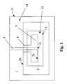
- Fig. 1 the top of the multilayer ceramic is shown in plan view.
- reference number 1 is the surface of the first dielectric layer 14 of the multilayer ceramic 6 designated.
- metallic coating on the multilayer ceramic 6 designated with reference number 2.
- the metallic coating 2 has a first recess 5 in the region of the opening of the dielectric-filled waveguide 15, which through the via rows executed in the layers (not shown) of the multilayer ceramic 6 12 is formed.
- Another recess 4 runs from the inside 2a to Outside 2b of the metallic coating 2.
- the microstrip line 3 runs from a base point 2c on the inside 2a of FIG Coating 2, which is on the opposite inside 2a of the recess 4 is located without contact with the coating 2 through the recess 4 to the Edge of the multilayer ceramic 6. This creates a coplanar line in the recess 4 and generates a slot line in the recess 5.
- FIG. 2 shows a side view of a waveguide-microstrip line transition according to the invention with an integrated choke structure.
- the multilayer ceramic 6 with the metallic coating 2 and the microstrip line 3 is separated from a gap 9, above a further waveguide 7.
- Two choke channels 8 are arranged on two opposite side walls of the waveguide 7.
- the choke channels 8 are arranged such that the opening 16 of the choke channels 8 facing the multilayer ceramic 6 closes with the opening (not shown) of the second waveguide 7.
- the opening 10 of the choke channels 8 facing away from the multilayer ceramic 6 is short-circuited.
- the vias 11 present in the multilayer ceramic 6 are shown in FIG are arranged in rows 12, shown.
- the Via Researchn 12 are for improvement the shielding of the high-frequency radiation is carried out twice.
- through the vias 11 in the vias 12 are in the multilayer ceramic 6 the dielectric filled Waveguide 15 formed.
- Fig. 3 shows a schematic representation of the multilayer ceramic in side view with the staggered rows of vias.
- the multilayer ceramic 6 is alternating layers of dielectric 14 and conductive Layers 13 built.
- Vias 11 are present in the dielectric layers, those in the respective layer form a row of vias 12.
- the vias 11 are arranged such that in neighboring ones dielectric layers 14 which vias are staggered, i.e. the vias 11 of the rows of vias 12 do not lie one above the other in a flight. This will make the Strength of the multilayer ceramic 6 increased.
- the multilayer ceramic 6 shown in FIG. 3 has 4 dielectric layers 14 and thus 4 mutually offset rows of rows 12. Of course it is also possible to use a multilayer ceramic with more than 4 layers.
- conductive layers 13 e.g. Metal layers, present, whereby the vias 11 of the rows of vias 12 are conductively connected to one another.
Landscapes
- Waveguides (AREA)
Abstract
Description
- Fig. 1
- in Draufsicht die Oberseite der Mehrlagenkeramik mit Mikrostreifenleitung, Koplanarleitung und Schlitzleitung.
- Fig. 2
- in Seitenansicht einen erfindungsgemäßen Hohlleiter-Mikrostreifen-Übergang mit integrierter Chokestruktur.
- Fig. 3
- eine schematisierte Darstellung der Mehrlagenkeramik in Seitenansicht mit den versetzt zueinander angeordneten Viareihen.
Die Chokekanäle 8 sind dabei derart angeordnet, dass die der Mehrlagenkeramik 6 zugewandte Öffnung 16 der Chokekanäle 8 mit der Öffnung (nicht dargestellt) des zweiten Hohlleiters 7 abschließt. Die der Mehrlagenkeramik 6 abgewandte Öffnung 10 der Chokekanäle 8 ist kurzgeschlossen.
Claims (7)
- Hohlleiter-Mikrostreifenleitungs-Übergang für elektromagnetische Wellen im Mikrowellen- und Millimeterwellenbereich, umfassenddadurch gekennzeichnet, dass die Mikrostreifenleitung (3) in der Aussparung (4, 5) auf der Oberseite (1) der ersten dielektrischen Schicht (14) derart angeordnet ist, dass in der einen Aussparung (4) eine Koplanarleitung und in der anderen Aussparung (5) über der Öffnung des dielektrisch gefüllten Hohlleiters (15) eine Schlitzleitung entsteht, wobei eine elektromagnetische Welle von der Mikrostreifenleitung (3) über die Koplanarleitung zur Schlitzleitung gelangt und von dort ohne Abstrahlung von Hochfrequenz in den dielektrisch gefüllten Hohlleiter (15) einkoppelbar ist und dass in einem Abstand (9) zwischen 0,02 mm und 1,0 mm, insbesondere 0,5 mm, unterhalb des in der Mehrlagenkeramik (6) dielektrisch gefüllten Hohlleiters (15) eine Öffnung eines zweiten Hohlleiters (7) angeordnet ist, wobei dieser zweite Hohlleiter (7) eine Chokestruktur aufweist.eine aus einer ersten und mindestens einer zweiten dielektrischen Schicht (14) mit dazwischen liegenden leitenden Schichten (13) aufgebauten Mehrlagenkeramik (6), wobei die dielektrischen Schichten (14) eine low temperature co-fired ceramic umfassen,in den dielektrischen Schichten (14) ausgeführte Vias (11), die als eine oder mehrere Viareihen (12) angeordnet, einen dielektrisch gefüllten Hohlleiter (15) bilden,eine leitfähige Beschichtung (2) auf der Oberseite (1) der ersten dielektrischen Schicht (14), welche Aussparungen im Bereich der Öffnung des dielektrisch gefüllten Hohlleiters (15) aufweist,eine Mikrostreifenleitung (3) auf der Oberseite (1) der ersten dielektrischen Schicht (14),
- Hohlleiter-Mikrostreifenleitungs-Übergang nach Anspruch 1, dadurch gekennzeichnet, dass zwei Chokekanäle (8) an gegenüberliegenden Außenwänden des zweiten Hohlleiters vorhanden sind, wobei die eine Öffnung (16) der Chokekanäle (8) mit der Öffnung des zweiten Hohlleiters (7) abschließt und die andere Öffnung (10) der Chokekanäle (8) kurzgeschlossen ist.
- Hohlleiter-Mikrostreifenleitungs-Übergang nach einem der vorangehenden Ansprüche, dadurch gekennzeichnet, dass die geometrische Länge der Chokekanäle (8) vom kurzgeschlossenen Ende (10) bis zur Öffnung des zweiten Hohlleiters eine halbe Hohlleiterwellenlänge des zweiten Hohlleiters (7) beträgt.
- Hohlleiter-Mikrostreifenleitungs-Übergang nach Anspruch 3, dadurch gekennzeichnet, dass die Chokekanäle (8) mit einem Dielektrikum gefüllt sind.
- Hohlleiter-Mikrostreifenleitungs-Übergang nach einem der vorangehenden Ansprüche, dadurch gekennzeichnet, dass der Abstand der Vias (11) in den Viareihen (12) kleiner als ein Zehntel der Hohlleiterwellenlänge ist.
- Hohlleiter-Mikrostreifenleitungs-Übergang nach einem der vorangehenden Ansprüche, dadurch gekennzeichnet, dass die Viareihen (12) in benachbarten dielektrischen Lagen (14) der Mehrlagenkeramik (6) übereinander und versetzt zueinander angeordnet sind.
- Verwendung des Hohlleiter-Mikrostreifenleitungs-Übergang nach einem der vorangehenden Ansprüche in einem Frequenzbereich von 1 GHz bis 50 GHz.
Applications Claiming Priority (2)
| Application Number | Priority Date | Filing Date | Title |
|---|---|---|---|
| DE10134204 | 2001-07-13 | ||
| DE2001134204 DE10134204C1 (de) | 2001-07-13 | 2001-07-13 | Hohlleiter-Mikrostreifen-Übergang |
Publications (2)
| Publication Number | Publication Date |
|---|---|
| EP1276169A2 true EP1276169A2 (de) | 2003-01-15 |
| EP1276169A3 EP1276169A3 (de) | 2003-05-28 |
Family
ID=7691740
Family Applications (1)
| Application Number | Title | Priority Date | Filing Date |
|---|---|---|---|
| EP02010542A Withdrawn EP1276169A3 (de) | 2001-07-13 | 2002-05-10 | Hohlleiter-Mikrostreifen-Übergang |
Country Status (2)
| Country | Link |
|---|---|
| EP (1) | EP1276169A3 (de) |
| DE (1) | DE10134204C1 (de) |
Cited By (2)
| Publication number | Priority date | Publication date | Assignee | Title |
|---|---|---|---|---|
| US7752911B2 (en) | 2005-11-14 | 2010-07-13 | Vega Grieshaber Kg | Waveguide transition for a fill level radar |
| US10826165B1 (en) | 2019-07-19 | 2020-11-03 | Eagle Technology, Llc | Satellite system having radio frequency assembly with signal coupling pin and associated methods |
Families Citing this family (1)
| Publication number | Priority date | Publication date | Assignee | Title |
|---|---|---|---|---|
| US7276987B2 (en) * | 2002-10-29 | 2007-10-02 | Kyocera Corporation | High frequency line-to-waveguide converter and high frequency package |
Citations (2)
| Publication number | Priority date | Publication date | Assignee | Title |
|---|---|---|---|---|
| US5781087A (en) * | 1995-12-27 | 1998-07-14 | Raytheon Company | Low cost rectangular waveguide rotary joint having low friction spacer system |
| US5912598A (en) * | 1997-07-01 | 1999-06-15 | Trw Inc. | Waveguide-to-microstrip transition for mmwave and MMIC applications |
Family Cites Families (3)
| Publication number | Priority date | Publication date | Assignee | Title |
|---|---|---|---|---|
| JP3493265B2 (ja) * | 1996-09-30 | 2004-02-03 | 京セラ株式会社 | 誘電体導波管線路および配線基板 |
| JP3464117B2 (ja) * | 1997-04-25 | 2003-11-05 | 京セラ株式会社 | 積層型共振器および積層型フィルタ |
| US5982250A (en) * | 1997-11-26 | 1999-11-09 | Twr Inc. | Millimeter-wave LTCC package |
-
2001
- 2001-07-13 DE DE2001134204 patent/DE10134204C1/de not_active Expired - Fee Related
-
2002
- 2002-05-10 EP EP02010542A patent/EP1276169A3/de not_active Withdrawn
Patent Citations (2)
| Publication number | Priority date | Publication date | Assignee | Title |
|---|---|---|---|---|
| US5781087A (en) * | 1995-12-27 | 1998-07-14 | Raytheon Company | Low cost rectangular waveguide rotary joint having low friction spacer system |
| US5912598A (en) * | 1997-07-01 | 1999-06-15 | Trw Inc. | Waveguide-to-microstrip transition for mmwave and MMIC applications |
Cited By (2)
| Publication number | Priority date | Publication date | Assignee | Title |
|---|---|---|---|---|
| US7752911B2 (en) | 2005-11-14 | 2010-07-13 | Vega Grieshaber Kg | Waveguide transition for a fill level radar |
| US10826165B1 (en) | 2019-07-19 | 2020-11-03 | Eagle Technology, Llc | Satellite system having radio frequency assembly with signal coupling pin and associated methods |
Also Published As
| Publication number | Publication date |
|---|---|
| DE10134204C1 (de) | 2002-09-12 |
| EP1276169A3 (de) | 2003-05-28 |
Similar Documents
| Publication | Publication Date | Title |
|---|---|---|
| DE69802467T2 (de) | Leiterplatte mit einer Übertragungsleitung für hohe Frequenzen | |
| DE69823591T2 (de) | Geschichtete Aperturantenne und mehrschichtige Leiterplatte damit | |
| EP1547192B1 (de) | Vorrichtung zum übertragen bzw. abstrahlen hochfrequenter wellen | |
| DE10350346B4 (de) | Hochfrequenzleitungs-Wellenleiter-Konverter und Hochfrequenzpaket | |
| DE69938271T2 (de) | Hochfrequenzmodul | |
| DE69835633T2 (de) | Hochfrequenzbaugruppe | |
| DE102017103161B4 (de) | Antennenvorrichtung und Antennenarray | |
| DE60026388T2 (de) | Spannungsgesteuerte koplanare Phasenschieber | |
| DE60308599T2 (de) | Hocheffiziente interdigitale Filter | |
| DE69828249T2 (de) | Hochfrequenzübertragungsleitung, dielektrischer Resonator, Filter, Duplexer und Kommunikationsgerät | |
| DE4407251C2 (de) | Dielektrischer Wellenleiter | |
| DE69623220T2 (de) | Dielektrischer Wellenleiter | |
| DE69830765T2 (de) | Dielektrische Wellenleiter | |
| DE112009001891T5 (de) | Hochfrequenzsubstrat und Hochfrequenzmodul | |
| DE10050544B4 (de) | Nicht strahlender dielektrischer Wellenleiter | |
| EP2991159B1 (de) | Speisenetzwerk für antennensysteme | |
| DE69711327T2 (de) | Gerät mit dielektrischem Resonator und Hochfrequenzmodul | |
| DE10008018A1 (de) | Dielektrischer Resonator, Induktor, Kondensator, Dielektrisches Filter, Oszillator und Kommunikationsvorrichtung | |
| DE69121549T2 (de) | Bandpassfilter | |
| DE69934749T2 (de) | Wandler für elektrisch transversale oder quasi-transversale Moden in Hohlleitermoden | |
| DE69829327T2 (de) | Dielektrisches Filter, Sende/Empfangsweiche, und Kommunikationsgerät | |
| DE60300040T2 (de) | Dielektrischer Resonator mit einer planaren dielektrischen Übertragungsleitung und Filter und Oszillator mit einem solchen Resonator | |
| DE60038079T2 (de) | Dielektrische Resonanzvorrichtung, dielektrisches Filter, zusammengestellte dielektrische Filtervorrichtung, dielektrischer Duplexer und Kommunikationsgerät | |
| DE10134204C1 (de) | Hohlleiter-Mikrostreifen-Übergang | |
| DE68916594T2 (de) | Mehrflächiger Wellenleiterkoppler. |
Legal Events
| Date | Code | Title | Description |
|---|---|---|---|
| PUAI | Public reference made under article 153(3) epc to a published international application that has entered the european phase |
Free format text: ORIGINAL CODE: 0009012 |
|
| AK | Designated contracting states |
Kind code of ref document: A2 Designated state(s): AT BE CH CY DE DK ES FI FR GB GR IE IT LI LU MC NL PT SE TR |
|
| AX | Request for extension of the european patent |
Free format text: AL;LT;LV;MK;RO;SI |
|
| PUAL | Search report despatched |
Free format text: ORIGINAL CODE: 0009013 |
|
| AK | Designated contracting states |
Designated state(s): AT BE CH CY DE DK ES FI FR GB GR IE IT LI LU MC NL PT SE TR |
|
| AX | Request for extension of the european patent |
Extension state: AL LT LV MK RO SI |
|
| 17P | Request for examination filed |
Effective date: 20030620 |
|
| AKX | Designation fees paid |
Designated state(s): AT BE CH CY DE DK ES FI FR GB GR IE IT LI LU MC NL PT SE TR |
|
| GRAP | Despatch of communication of intention to grant a patent |
Free format text: ORIGINAL CODE: EPIDOSNIGR1 |
|
| STAA | Information on the status of an ep patent application or granted ep patent |
Free format text: STATUS: THE APPLICATION IS DEEMED TO BE WITHDRAWN |
|
| 18D | Application deemed to be withdrawn |
Effective date: 20061205 |