EP1276147A2 - Dual hardmask process for the formation of copper/low-K interconnects - Google Patents
Dual hardmask process for the formation of copper/low-K interconnects Download PDFInfo
- Publication number
- EP1276147A2 EP1276147A2 EP02100795A EP02100795A EP1276147A2 EP 1276147 A2 EP1276147 A2 EP 1276147A2 EP 02100795 A EP02100795 A EP 02100795A EP 02100795 A EP02100795 A EP 02100795A EP 1276147 A2 EP1276147 A2 EP 1276147A2
- Authority
- EP
- European Patent Office
- Prior art keywords
- layer
- hardmask
- dielectric layer
- dielectric
- forming
- Prior art date
- Legal status (The legal status is an assumption and is not a legal conclusion. Google has not performed a legal analysis and makes no representation as to the accuracy of the status listed.)
- Withdrawn
Links
Images



Classifications
-
- H—ELECTRICITY
- H10—SEMICONDUCTOR DEVICES; ELECTRIC SOLID-STATE DEVICES NOT OTHERWISE PROVIDED FOR
- H10W—GENERIC PACKAGES, INTERCONNECTIONS, CONNECTORS OR OTHER CONSTRUCTIONAL DETAILS OF DEVICES COVERED BY CLASS H10
- H10W20/00—Interconnections in chips, wafers or substrates
- H10W20/01—Manufacture or treatment
- H10W20/071—Manufacture or treatment of dielectric parts thereof
- H10W20/081—Manufacture or treatment of dielectric parts thereof by forming openings in the dielectric parts
- H10W20/084—Manufacture or treatment of dielectric parts thereof by forming openings in the dielectric parts for dual-damascene structures
- H10W20/087—Manufacture or treatment of dielectric parts thereof by forming openings in the dielectric parts for dual-damascene structures involving multiple stacked pre-patterned masks
-
- H—ELECTRICITY
- H10—SEMICONDUCTOR DEVICES; ELECTRIC SOLID-STATE DEVICES NOT OTHERWISE PROVIDED FOR
- H10P—GENERIC PROCESSES OR APPARATUS FOR THE MANUFACTURE OR TREATMENT OF DEVICES COVERED BY CLASS H10
- H10P50/00—Etching of wafers, substrates or parts of devices
- H10P50/73—Etching of wafers, substrates or parts of devices using masks for insulating materials
-
- H—ELECTRICITY
- H10—SEMICONDUCTOR DEVICES; ELECTRIC SOLID-STATE DEVICES NOT OTHERWISE PROVIDED FOR
- H10W—GENERIC PACKAGES, INTERCONNECTIONS, CONNECTORS OR OTHER CONSTRUCTIONAL DETAILS OF DEVICES COVERED BY CLASS H10
- H10W20/00—Interconnections in chips, wafers or substrates
- H10W20/01—Manufacture or treatment
- H10W20/071—Manufacture or treatment of dielectric parts thereof
- H10W20/081—Manufacture or treatment of dielectric parts thereof by forming openings in the dielectric parts
- H10W20/084—Manufacture or treatment of dielectric parts thereof by forming openings in the dielectric parts for dual-damascene structures
- H10W20/088—Manufacture or treatment of dielectric parts thereof by forming openings in the dielectric parts for dual-damascene structures involving partial etching of via holes
Definitions
- the invention is generally related to the field of semiconductor devices and fabrication and more specifically to a method for forming copper lines in integrated circuits using a dual hardmask process.
- an ILD layer is deposited first, followed by an IMD deposition.
- An IMD etch-stop layer such as SiN or SiC, can be optionally used in between IMD and ILD.
- a via is patterned and etched through the IMD and ILD for connection to lower interconnect levels.
- a trench is patterned and etched in the IMD.
- a barrier layer and a copper seed layer are then deposited over the structure.
- the barrier layer is typically tantalum nitride or some other binary transition metal nitride.
- the copper layer is electrochemically deposited (ECD) using the seed layer over the entire structure.
- the copper is then chemically-mechanically polished (CMP'd) to remove the copper over the IMD, leaving copper interconnect lines and vias.
- the present invention describes a dual hardmask process for forming integrated circuit interconnects. Multiple hardmask layers are formed on the upper surface of a single or multiple dielectric layer(s). The dielectric layer or layers is/are formed over a silicon wafer containing numerous electronic devices. A first hardmask is formed on the dielectric layer. This first hardmask comprises silicon carbide or silicon nitride. A second hardmask layer is formed on the first hardmask layer.
- the second hardmask layer comprises a material selected from the group consisting of titanium aluminide (TiAl), titanium aluminum nitride (TiAlN), titanium nitride (TiN), aluminum nitride (AlN), tantalum aluminide (TaAl), and tantalum aluminum nitride (TaAlN).
- TiAl titanium aluminide
- TiAlN titanium aluminum nitride
- TiN titanium nitride
- AlN aluminum nitride
- TaAl tantalum aluminide
- TaAlN tantalum aluminum nitride
- TaAlN tantalum aluminum nitride
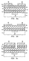
- an etch stop layer 30 is formed over a copper layer 20 and a dielectric layer 10.
- the dielectric layer 10 is formed over a silicon substrate containing various electronic devices such as transistors, diodes, etc.
- the copper layer 20 represents a portion of the copper interconnect of an integrated circuit which is made up of the electronic devices contained in the silicon substrate.
- the etch stop layer may comprise silicon nitride (SiN), silicon carbide (SiC), or any suitable material with good etch selectivity and preferably low dielectric constant.
- a low k dielectric layer 40 with a low dielectric constant i.e. less that 3.0 is formed over the etch stop layer 30.
- this low k dielectric layer 40 comprises organosilicate glass (OSG) which has a dielectric constant of about 2.8.
- OSG organosilicate glass
- any suitable low k dielectric material may be used to form the dielectric layer 40.
- a first hardmask layer 50 is formed.
- This first hardmask layer 50 comprises a material selected -from the group consisting of silicon carbide (SiC), silicon nitride (SiN), and any other suitable material.
- a second hardmask layer 60 is formed over the first hardmask layer.
- This second hardmask layer comprises a material selected from the group consisting of titanium aluminide (TiAl), titanium aluminum nitride (TiAlN), titanium nitride (TiN), aluminum nitride (AlN), tantalum aluminide (TaAl), tantalum aluminum nitride (TaAlN), or any combination of layers of these various alloys.
- Ti (1-x) Al x N is used with x varying from 0 to 100% and more preferably from 25% to 40%. For a Ti (1-x) Al x N film where x varies from 25% to 40% the etch rate selectivity of OSG to Ti (1-x) Al x N is approximately 15:1.
- the OSG layer will etch about fifteen times faster than the Ti (1-x) Al x N layer.
- a layer of bottom antireflective coating (BARC) 70 and a photoresist layer 80 are formed and patterned as shown in Figure 1(a).
- the BARC layer 70 is an optional layer.
- FIG. 1(b) Shown in Figure 1(b) is the structure of Figure 1(a) following the etching of the BARC layer 70 and the second hardmask layer 60 with the remaining photoresist and BARC stripped.
- the Ti (1-x) Al x N second hardmask layer 60 is etched with a dry plasma etch process comprising BCl 3 ,Cl 2 and other additives such as N2 and Ar, and a plasma source power of approximately 800 Watts to 1500 Watts, and a bias power of approximately 50-250 Watts.
- the flow rates of BCl 3 and Cl 2 are 0-150 sccm and 50-200 sccm respectively and the chamber pressure is approximately 5 mTorr to 20 mTorr.
- the resist 80 and BARC 70 are stripped away in an oxygen-based plasma.
- Alternative plasma such as H 2 and/or N 2 , maybe used for photoresist strip.
- a wet clean is optional to remove possible residues.
- a second BARC layer 75 and a second photoresist layer 85 are formed and patterned on the structure of Figure 1(b) to define the first trench pattern as shown in Figure 1(c).
- BARC layer 75 is etched and the exposed portion of the first hardmask layer 50 and the underlying low k dielectric layer 40 are etched to form a first trench as shown in Figure 1(c).
- a C 4 F 8 /N 2 /CO plasma based process can be used with flow rates of 5-10 sccm (C 4 F 8 ), 50-300 sccm (N 2 ), and 50-200 sccm (CO) with a plasma power source of approximately 900 Watts to 2000 Watts.
- the photoresist layer 85 will be attacked during the etching processes and will be wholly or partially removed. Following the etching of the OSG film 40, the remaining photoresist layer 85, BARC layer 75, and exposed region of the first hardmask layer 50 are removed resulting in the structure illustrated in Figure 1(d). Alternatively, the photoresist layer 85 and BARC 75 can be stripped before the start of the etching of dielectric layer 40, to reduce the undesired impact to the low k dielectrics 40.
- the exposed region of the low k dielectric layer is then etched as shown in Figure 1(e) to form a second trench structure which is positioned over the first trench structure.
- the exposed portion of the etch stop layer 30 is removed and a liner layer 90 and copper region 100 is formed as shown in Figure 1(f).
- Standard semiconductor process techniques can be used to form the liner layer 90 and copper region 100 such as film deposition and chemical mechanical polishing (CMP).
- CMP chemical mechanical polishing
- the hardmask layers 50 and 60 can be removed using CMP.
- the copper region 100 is formed by first forming a thick layer of copper followed by CMP processes to remove the excess copper. The removal of the hardmask layers 50 and 60 using CMP can be incorporated into this copper CMP removal process by changing the polishing conditions.
- any suitable conducting material can be used to fill the trench formed in the low k dielectric.
- FIG. 2(a) - 2(g) A further embodiment of the instant invention is shown in Figures 2(a) - 2(g).
- a first etch stop layer 30 is formed over a copper layer 20 and a first dielectric layer 10.
- the dielectric layer 10 is formed over a silicon substrate containing various electronic devices such as transistors, diodes, etc.
- the copper layer 20 represents a portion of the copper interconnect of an integrated circuit which is made up of the electronic devices contained in the silicon substrate.
- layers 10 and 20 described here generally represent the previous interconnect level.
- the first etch stop layer may comprise silicon nitride (SiN), silicon carbide (SiC), or any suitable material.
- a first dielectric layer 42 with a low dielectric constant (i.e. less that 3.0) is formed over the etch stop layer 30.
- this low k dielectric layer 42 comprises organosilicate glass (OSG) which has a dielectric constant of about 2.8.
- OSG organosilicate glass
- any suitable low k dielectric material may be used to form the first dielectric layer 42.
- a second etch stop layer 110 is formed on the first low k dielectric layer 42.
- the second etch stop layer may comprise silicon nitride (SiN), silicon carbide (SiC), or any suitable material.
- a second low k dielectric film i.e.
- first hardmask layer 50 is formed on the second low k dielectric film 44.
- This first hardmask layer 50 comprises a material selected from the group consisting of silicon carbide (SiC), silicon nitride (SiN), and any other suitable material.
- a second hardmask layer 60 is formed on the first hardmask layer.
- This second hardmask layer comprises a material selected from the group consisting of titanium aluminide (TiAl), titanium aluminum nitride (TiAlN), titanium nitride (TiN), aluminum nitride (AlN), tantalum aluminide (TaAl), tantalum aluminum nitride (TaAlN), or any combination of layers of these various alloys.
- Ti (1-x) Al x N is used with x varying from 0 to 100% and more preferably from 25% to 40%. For a Ti (1-x) Al x N film where x varies from 25% to 40% the etch rate selectivity of OSG to Ti (1-x) Al x N is approximately 15:1.
- the OSG film will etch approximately fifteen times faster than the Ti (1-x) Al x N film.
- a layer of bottom antireflective coating (BARC) 70 and a photoresist layer 80 is formed and patterned as shown in Figure 2(a).
- the BARC 70 is an optional layer.
- FIG. 2(b) Shown in Figure 2(b) is the structure of Figure 2(a) following the etching of the BARC layer 70 and the second hardmask layer 60 followed by resist and BARC stripping.
- the Ti (1-x) Al x N second hardmask layer 60 is etched with a dry plasma etch process comprising BCl 3 , Cl 2 and other additives such as N2 and Ar, and a plasma source power of approximately 800 Watts to 1500 Watts, and a bias power of approximately 50-250 Watts.
- the flow rates of BCl 3 and Cl 2 are 0-150 sccm and 50-200 sccm, respectively and the chamber pressure is approximately 5-20 mTorr.
- the resist 80 and BARC 70 are stripped away in an oxygen-based plasma.
- Alternative plasma such as H 2 and/or N 2 , may also be used for photoresist strip.
- a wet clean is optional to remove possible residues.
- a second BARC layer 75 and a second photoresist layer 85 are formed and patterned on the structure of Figure 2(b) as shown in Figure 2(c).
- the exposed portion of the first hardmask layer 50 is etched and the resist 85 and BARC 75 layers are stripped in an H 2 or N 2 plasma.
- Oxygen plasma may need to be avoided for resist strip if it changes the properties of the low k dielectric layer 44.
- a wet clean is optional after resist strip to remove any etch residues. In the case of via-to-trench misalignment, an additional second hardmask etch is needed prior to the first hardmask via opening etch.
- the low k dielectric layer 44 is etched as shown in Figure 2(d).
- a C 4 F 8 /N 2 /CO plasma based process can be used with flow rates of 5-10 sccm C 4 F 8 , 50-300 sccm N 2 , and 50-200 sccm CO with a plasma power source of approximately 900 Watts to 2000 Watts.
- the exposed region of the second etch stop layer 110 and the exposed portion of the first hardmask 50 are now removed using the second hardmask 60 as etch mask as shown in Fig 2(e).
- the exposed portions of the low k dielectric layers 44 and 42 are then etched simultaneously.
- the etching process is completed when the etch stop layer 110 is reached in the trench portion and etch stop layer 30 is reached in the via portion as shown in Fig 2(f).
- the exposed portion of the etch stop layer 30 is removed, and the exposed portion of the trench etch stop layer 110 may be etched as well.
- a liner layer 90 and copper region 100 is formed as shown in Figure 2(g). Standard semiconductor process techniques can be used to form the liner layer 90 and copper region 100 such as film deposition and chemical mechanical polishing (CMP).
- CMP chemical mechanical polishing
- the hardmask layers 50 and 60 can be removed using CMP.
- the copper region 100 is formed by first forming a thick layer of copper followed by CMP processes to remove the excess copper.
- the removal of the hardmask layers 50 and 60 using CMP can be incorporated into this copper CMP removal process by changing the polishing conditions.
- any suitable conducting material can be used to fill the various trench structures.
Landscapes
- Internal Circuitry In Semiconductor Integrated Circuit Devices (AREA)
- Drying Of Semiconductors (AREA)
Abstract
Description
Claims (8)
- A method for forming interconnects, comprising:providing a silicon substrate containing one or more electronic devices;forming a first dielectric layer over said silicon substrate;forming a second dielectric layer over said first dielectric layer wherein the dielectric constant of the second dielectric layer is less that 3.0;forming a first hardmask layer over said second dielectric layer;forming a second hardmask layer on said first hardmask layer wherein said second hardmask layer comprises a material selected from the group consisting of titanium aluminide (TiAl), titanium aluminum nitride (TiAlN), titanium nitride (TiN), aluminum nitride (AlN), tantalum aluminide (TaAl), and tantalum aluminum nitride (TaAlN);forming a trench in said second dielectric; andfilling said trench with a conducting material.
- The method of claim 1 wherein said second dielectric layer is OSG.
- The method of claim 1 or Claim 2 wherein said conducting material is copper.
- The method of any preceding claim, wherein the material used to form the first hardmask layer is selected from the group consisting of silicon carbide and silicon nitride.
- A method for forming interconnects, comprising:providing a silicon substrate containing one or more electronic devices;forming a first dielectric layer over said silicon substrate;forming a second dielectric layer over said first dielectric layer wherein the dielectric constant of the second dielectric layer is less that 3.0;forming a first hardmask layer over said second dielectric layer;forming a second hardmask layer on said first hardmask layer wherein said second hardmask layer comprises a material selected from the group consisting of titanium aluminide (TiAl), titanium aluminum nitride (TiAlN), titanium nitride (TiN), aluminum nitride (AlN), tantalum aluminide (TaAl), and tantalum aluminum nitride (TaAlN);etching a first opening in said second hardmask layer of a first width;forming a first trench of a second width in said second dielectric layer wherein said second width is less than said first width;etching a second opening in said first hardmask layer of a first width;forming a second trench of a first width in said second dielectric layer wherein said second trench is positioned over said first trench; andfilling said first and second trench with a conducting material.
- The method of claim 5 wherein said second dielectric layer is OSG.
- The method of claim 5 or claim 6, wherein said conducting material is copper.
- The method of claim 5, claim 6 or claim 7, wherein said first hardmask is a material selected from the group consisting of silicon nitride and silicon carbide.
Applications Claiming Priority (2)
| Application Number | Priority Date | Filing Date | Title |
|---|---|---|---|
| US09/901,416 US20030008490A1 (en) | 2001-07-09 | 2001-07-09 | Dual hardmask process for the formation of copper/low-k interconnects |
| US901416 | 2001-07-09 |
Publications (2)
| Publication Number | Publication Date |
|---|---|
| EP1276147A2 true EP1276147A2 (en) | 2003-01-15 |
| EP1276147A3 EP1276147A3 (en) | 2003-07-02 |
Family
ID=25414132
Family Applications (1)
| Application Number | Title | Priority Date | Filing Date |
|---|---|---|---|
| EP02100795A Withdrawn EP1276147A3 (en) | 2001-07-09 | 2002-07-09 | Dual hardmask process for the formation of copper/low-K interconnects |
Country Status (3)
| Country | Link |
|---|---|
| US (1) | US20030008490A1 (en) |
| EP (1) | EP1276147A3 (en) |
| JP (1) | JP2003100871A (en) |
Cited By (2)
| Publication number | Priority date | Publication date | Assignee | Title |
|---|---|---|---|---|
| FR2872342A1 (en) * | 2004-06-28 | 2005-12-30 | Semiconductor Leading Edge Tec | METHOD FOR MANUFACTURING A SEMICONDUCTOR DEVICE |
| DE102005030588A1 (en) * | 2005-06-30 | 2007-01-04 | Advanced Micro Devices, Inc., Sunnyvale | A technique for reducing etch damage during the fabrication of vias and trenches in interlayer dielectrics |
Families Citing this family (37)
| Publication number | Priority date | Publication date | Assignee | Title |
|---|---|---|---|---|
| US6696222B2 (en) * | 2001-07-24 | 2004-02-24 | Silicon Integrated Systems Corp. | Dual damascene process using metal hard mask |
| JP2003077920A (en) * | 2001-09-04 | 2003-03-14 | Nec Corp | Method of forming metal wiring |
| US6555467B2 (en) * | 2001-09-28 | 2003-04-29 | Sharp Laboratories Of America, Inc. | Method of making air gaps copper interconnect |
| KR100428791B1 (en) * | 2002-04-17 | 2004-04-28 | 삼성전자주식회사 | Method of forming dual damascene interconnection using low dielectric material |
| TW546771B (en) * | 2002-05-13 | 2003-08-11 | Nanya Technology Corp | Manufacturing method of dual damascene structure |
| KR100454130B1 (en) * | 2002-05-28 | 2004-10-26 | 삼성전자주식회사 | Method of forming dual damascene interconnection using low dielectric material |
| US6797630B1 (en) * | 2002-06-28 | 2004-09-28 | Taiwan Semiconductor Manufacturing Company, Ltd. | Partial via hard mask open on low-k dual damascene etch with dual hard mask (DHM) approach |
| US7214609B2 (en) | 2002-12-05 | 2007-05-08 | Texas Instruments Incorporated | Methods for forming single damascene via or trench cavities and for forming dual damascene via cavities |
| DE10301243B4 (en) * | 2003-01-15 | 2009-04-16 | Infineon Technologies Ag | Method for producing an integrated circuit arrangement, in particular with capacitor arrangement |
| US7052621B2 (en) * | 2003-06-13 | 2006-05-30 | Infineon Technologies Ag | Bilayered metal hardmasks for use in Dual Damascene etch schemes |
| US7915085B2 (en) * | 2003-09-18 | 2011-03-29 | Cree, Inc. | Molded chip fabrication method |
| US20050245074A1 (en) * | 2004-04-29 | 2005-11-03 | Ping Jiang | In-situ etch-stop etch and ashing in association with damascene processing in forming semiconductor interconnect structures |
| US7531448B2 (en) * | 2005-06-22 | 2009-05-12 | United Microelectronics Corp. | Manufacturing method of dual damascene structure |
| US20070093069A1 (en) * | 2005-10-21 | 2007-04-26 | Chien-Hua Tsai | Purge process after dry etching |
| US7358182B2 (en) * | 2005-12-22 | 2008-04-15 | International Business Machines Corporation | Method of forming an interconnect structure |
| US7435676B2 (en) * | 2006-01-10 | 2008-10-14 | International Business Machines Corporation | Dual damascene process flow enabling minimal ULK film modification and enhanced stack integrity |
| KR100838395B1 (en) | 2006-02-27 | 2008-06-13 | 주식회사 하이닉스반도체 | Method for fabricating semiconductor device using hardmask |
| US7902066B2 (en) * | 2006-09-26 | 2011-03-08 | Chartered Semiconductor Manufacturing, Ltd. | Damascene contact structure for integrated circuits |
| US7977244B2 (en) * | 2006-12-18 | 2011-07-12 | United Microelectronics Corp. | Semiconductor manufacturing process |
| US8501395B2 (en) * | 2007-06-04 | 2013-08-06 | Applied Materials, Inc. | Line edge roughness reduction and double patterning |
| US7884019B2 (en) * | 2007-06-07 | 2011-02-08 | Texas Instruments Incorporated | Poison-free and low ULK damage integration scheme for damascene interconnects |
| US20090314743A1 (en) * | 2008-06-20 | 2009-12-24 | Hong Ma | Method of etching a dielectric layer |
| JP5834189B2 (en) * | 2010-10-07 | 2015-12-16 | パナソニックIpマネジメント株式会社 | Manufacturing method of semiconductor device |
| US8252699B2 (en) * | 2010-11-22 | 2012-08-28 | Applied Materials, Inc. | Composite removable hardmask |
| US8735283B2 (en) * | 2011-06-23 | 2014-05-27 | International Business Machines Corporation | Method for forming small dimension openings in the organic masking layer of tri-layer lithography |
| JP5936507B2 (en) * | 2012-09-27 | 2016-06-22 | ルネサスエレクトロニクス株式会社 | Manufacturing method of semiconductor device |
| JP6061610B2 (en) * | 2012-10-18 | 2017-01-18 | ルネサスエレクトロニクス株式会社 | Manufacturing method of semiconductor device |
| US9129965B2 (en) * | 2013-03-14 | 2015-09-08 | Taiwan Semiconductor Manufacturing Company, Ltd. | Semiconductor devices and methods of manufacture thereof |
| US9209136B2 (en) | 2013-04-01 | 2015-12-08 | Intel Corporation | Hybrid carbon-metal interconnect structures |
| KR102055206B1 (en) * | 2013-07-08 | 2019-12-12 | 삼성전자주식회사 | Method for decomposition of a layout and method for manufacturing a semiconductor device using for the same |
| US20150104938A1 (en) * | 2013-10-16 | 2015-04-16 | United Microelectronics Corporation | Method for forming damascene opening and applications thereof |
| US9087824B2 (en) * | 2013-12-17 | 2015-07-21 | Texas Instruments Incorporated | Use of dielectric slots for reducing via resistance in dual damascene process |
| US9287372B2 (en) * | 2013-12-27 | 2016-03-15 | Taiwan Semiconductor Manufacturing Company Limited | Method of forming trench on FinFET and FinFET thereof |
| CN104979273B (en) * | 2014-04-04 | 2018-02-16 | 中芯国际集成电路制造(上海)有限公司 | The method for forming interconnection structure |
| US9646876B2 (en) | 2015-02-27 | 2017-05-09 | Applied Materials, Inc. | Aluminum nitride barrier layer |
| WO2017049267A1 (en) | 2015-09-19 | 2017-03-23 | Applied Materials, Inc. | Titanium-compound based hard mask films |
| US10770344B2 (en) | 2019-01-09 | 2020-09-08 | Globalfoundries Inc. | Chamferless interconnect vias of semiconductor devices |
Family Cites Families (5)
| Publication number | Priority date | Publication date | Assignee | Title |
|---|---|---|---|---|
| US6340435B1 (en) * | 1998-02-11 | 2002-01-22 | Applied Materials, Inc. | Integrated low K dielectrics and etch stops |
| TW389988B (en) * | 1998-05-22 | 2000-05-11 | United Microelectronics Corp | Method for forming metal interconnect in dielectric layer with low dielectric constant |
| JP3657788B2 (en) * | 1998-10-14 | 2005-06-08 | 富士通株式会社 | Semiconductor device and manufacturing method thereof |
| US6060380A (en) * | 1998-11-06 | 2000-05-09 | Advanced Micro Devices, Inc. | Antireflective siliconoxynitride hardmask layer used during etching processes in integrated circuit fabrication |
| US6184142B1 (en) * | 1999-04-26 | 2001-02-06 | United Microelectronics Corp. | Process for low k organic dielectric film etch |
-
2001
- 2001-07-09 US US09/901,416 patent/US20030008490A1/en not_active Abandoned
-
2002
- 2002-07-09 JP JP2002199893A patent/JP2003100871A/en active Pending
- 2002-07-09 EP EP02100795A patent/EP1276147A3/en not_active Withdrawn
Cited By (5)
| Publication number | Priority date | Publication date | Assignee | Title |
|---|---|---|---|---|
| FR2872342A1 (en) * | 2004-06-28 | 2005-12-30 | Semiconductor Leading Edge Tec | METHOD FOR MANUFACTURING A SEMICONDUCTOR DEVICE |
| US7169708B2 (en) | 2004-06-28 | 2007-01-30 | Rohm Co., Ltd. | Semiconductor device fabrication method |
| DE102005030588A1 (en) * | 2005-06-30 | 2007-01-04 | Advanced Micro Devices, Inc., Sunnyvale | A technique for reducing etch damage during the fabrication of vias and trenches in interlayer dielectrics |
| US7309654B2 (en) | 2005-06-30 | 2007-12-18 | Advanced Micro Devices, Inc. | Technique for reducing etch damage during the formation of vias and trenches in interlayer dielectrics |
| DE102005030588B4 (en) * | 2005-06-30 | 2008-10-16 | Advanced Micro Devices, Inc., Sunnyvale | A technique for reducing etch damage during the fabrication of vias and trenches in interlayer dielectrics |
Also Published As
| Publication number | Publication date |
|---|---|
| EP1276147A3 (en) | 2003-07-02 |
| US20030008490A1 (en) | 2003-01-09 |
| JP2003100871A (en) | 2003-04-04 |
Similar Documents
| Publication | Publication Date | Title |
|---|---|---|
| US20030008490A1 (en) | Dual hardmask process for the formation of copper/low-k interconnects | |
| US6410426B1 (en) | Damascene cap layer process for integrated circuit interconnects | |
| US6274499B1 (en) | Method to avoid copper contamination during copper etching and CMP | |
| US6114243A (en) | Method to avoid copper contamination on the sidewall of a via or a dual damascene structure | |
| US8299617B2 (en) | Method and apparatus for forming metal-metal oxide etch stop/barrier for integrated circuit interconnects | |
| US7129162B2 (en) | Dual cap layer in damascene interconnection processes | |
| US7112532B2 (en) | Process for forming a dual damascene structure | |
| US6913994B2 (en) | Method to form Cu/OSG dual damascene structure for high performance and reliable interconnects | |
| US6713402B2 (en) | Methods for polymer removal following etch-stop layer etch | |
| US6228760B1 (en) | Use of PE-SiON or PE-OXIDE for contact or via photo and for defect reduction with oxide and W chemical-mechanical polish | |
| JP5391594B2 (en) | Manufacturing method of semiconductor device | |
| US20080176404A1 (en) | Method for fabricating semiconductor device | |
| US6376361B1 (en) | Method to remove excess metal in the formation of damascene and dual interconnects | |
| US6255226B1 (en) | Optimized metal etch process to enable the use of aluminum plugs | |
| JP2003179136A (en) | Mask layer and interconnect structure for dual damascene semiconductor fabrication | |
| JP2006128542A (en) | Manufacturing method of electronic device | |
| US6900123B2 (en) | BARC etch comprising a selective etch chemistry and a high polymerizing gas for CD control | |
| JP2006128541A (en) | Manufacturing method of electronic device | |
| JP2005005697A (en) | Manufacturing method of semiconductor device | |
| KR101138082B1 (en) | A method for forming a dual damascene pattern in semiconductor device | |
| US20080122107A1 (en) | Poly silicon hard mask | |
| JP4102159B2 (en) | Manufacturing method of semiconductor device | |
| KR100493937B1 (en) | Gap filling process for micro display device | |
| KR20050009798A (en) | Method for forming metal-line of the semiconductor device using dual damascene process | |
| JP2005093606A (en) | Method of manufacturing semiconductor device |
Legal Events
| Date | Code | Title | Description |
|---|---|---|---|
| PUAI | Public reference made under article 153(3) epc to a published international application that has entered the european phase |
Free format text: ORIGINAL CODE: 0009012 |
|
| AK | Designated contracting states |
Kind code of ref document: A2 Designated state(s): AT BE BG CH CY CZ DE DK EE ES FI FR GB GR IE IT LI LU MC NL PT SE SK TR |
|
| AX | Request for extension of the european patent |
Free format text: AL;LT;LV;MK;RO;SI |
|
| PUAL | Search report despatched |
Free format text: ORIGINAL CODE: 0009013 |
|
| AK | Designated contracting states |
Designated state(s): AT BE BG CH CY CZ DE DK EE ES FI FR GB GR IE IT LI LU MC NL PT SE SK TR |
|
| AX | Request for extension of the european patent |
Extension state: AL LT LV MK RO SI |
|
| 17P | Request for examination filed |
Effective date: 20040102 |
|
| AKX | Designation fees paid |
Designated state(s): DE FR GB |
|
| 17Q | First examination report despatched |
Effective date: 20040304 |
|
| STAA | Information on the status of an ep patent application or granted ep patent |
Free format text: STATUS: THE APPLICATION HAS BEEN WITHDRAWN |
|
| 18W | Application withdrawn |
Effective date: 20150929 |