EP1275697A1 - Curable composition, composition for optical material, optical material, liquid-crystal display, transparent conductive film, and process for producing the same - Google Patents
Curable composition, composition for optical material, optical material, liquid-crystal display, transparent conductive film, and process for producing the same Download PDFInfo
- Publication number
- EP1275697A1 EP1275697A1 EP01921977A EP01921977A EP1275697A1 EP 1275697 A1 EP1275697 A1 EP 1275697A1 EP 01921977 A EP01921977 A EP 01921977A EP 01921977 A EP01921977 A EP 01921977A EP 1275697 A1 EP1275697 A1 EP 1275697A1
- Authority
- EP
- European Patent Office
- Prior art keywords
- liquid crystal
- component
- crystal display
- optical material
- film
- Prior art date
- Legal status (The legal status is an assumption and is not a legal conclusion. Google has not performed a legal analysis and makes no representation as to the accuracy of the status listed.)
- Withdrawn
Links
Images
Classifications
-
- G—PHYSICS
- G02—OPTICS
- G02F—OPTICAL DEVICES OR ARRANGEMENTS FOR THE CONTROL OF LIGHT BY MODIFICATION OF THE OPTICAL PROPERTIES OF THE MEDIA OF THE ELEMENTS INVOLVED THEREIN; NON-LINEAR OPTICS; FREQUENCY-CHANGING OF LIGHT; OPTICAL LOGIC ELEMENTS; OPTICAL ANALOGUE/DIGITAL CONVERTERS
- G02F1/00—Devices or arrangements for the control of the intensity, colour, phase, polarisation or direction of light arriving from an independent light source, e.g. switching, gating or modulating; Non-linear optics
- G02F1/01—Devices or arrangements for the control of the intensity, colour, phase, polarisation or direction of light arriving from an independent light source, e.g. switching, gating or modulating; Non-linear optics for the control of the intensity, phase, polarisation or colour
- G02F1/13—Devices or arrangements for the control of the intensity, colour, phase, polarisation or direction of light arriving from an independent light source, e.g. switching, gating or modulating; Non-linear optics for the control of the intensity, phase, polarisation or colour based on liquid crystals, e.g. single liquid crystal display cells
- G02F1/133—Constructional arrangements; Operation of liquid crystal cells; Circuit arrangements
- G02F1/1333—Constructional arrangements; Manufacturing methods
- G02F1/1343—Electrodes
- G02F1/13439—Electrodes characterised by their electrical, optical, physical properties; materials therefor; method of making
-
- C—CHEMISTRY; METALLURGY
- C08—ORGANIC MACROMOLECULAR COMPOUNDS; THEIR PREPARATION OR CHEMICAL WORKING-UP; COMPOSITIONS BASED THEREON
- C08G—MACROMOLECULAR COMPOUNDS OBTAINED OTHERWISE THAN BY REACTIONS ONLY INVOLVING UNSATURATED CARBON-TO-CARBON BONDS
- C08G77/00—Macromolecular compounds obtained by reactions forming a linkage containing silicon with or without sulfur, nitrogen, oxygen or carbon in the main chain of the macromolecule
- C08G77/42—Block-or graft-polymers containing polysiloxane sequences
-
- C—CHEMISTRY; METALLURGY
- C08—ORGANIC MACROMOLECULAR COMPOUNDS; THEIR PREPARATION OR CHEMICAL WORKING-UP; COMPOSITIONS BASED THEREON
- C08G—MACROMOLECULAR COMPOUNDS OBTAINED OTHERWISE THAN BY REACTIONS ONLY INVOLVING UNSATURATED CARBON-TO-CARBON BONDS
- C08G77/00—Macromolecular compounds obtained by reactions forming a linkage containing silicon with or without sulfur, nitrogen, oxygen or carbon in the main chain of the macromolecule
- C08G77/48—Macromolecular compounds obtained by reactions forming a linkage containing silicon with or without sulfur, nitrogen, oxygen or carbon in the main chain of the macromolecule in which at least two but not all the silicon atoms are connected by linkages other than oxygen atoms
- C08G77/50—Macromolecular compounds obtained by reactions forming a linkage containing silicon with or without sulfur, nitrogen, oxygen or carbon in the main chain of the macromolecule in which at least two but not all the silicon atoms are connected by linkages other than oxygen atoms by carbon linkages
-
- G—PHYSICS
- G02—OPTICS
- G02B—OPTICAL ELEMENTS, SYSTEMS OR APPARATUS
- G02B1/00—Optical elements characterised by the material of which they are made; Optical coatings for optical elements
- G02B1/04—Optical elements characterised by the material of which they are made; Optical coatings for optical elements made of organic materials, e.g. plastics
-
- G—PHYSICS
- G02—OPTICS
- G02F—OPTICAL DEVICES OR ARRANGEMENTS FOR THE CONTROL OF LIGHT BY MODIFICATION OF THE OPTICAL PROPERTIES OF THE MEDIA OF THE ELEMENTS INVOLVED THEREIN; NON-LINEAR OPTICS; FREQUENCY-CHANGING OF LIGHT; OPTICAL LOGIC ELEMENTS; OPTICAL ANALOGUE/DIGITAL CONVERTERS
- G02F1/00—Devices or arrangements for the control of the intensity, colour, phase, polarisation or direction of light arriving from an independent light source, e.g. switching, gating or modulating; Non-linear optics
- G02F1/01—Devices or arrangements for the control of the intensity, colour, phase, polarisation or direction of light arriving from an independent light source, e.g. switching, gating or modulating; Non-linear optics for the control of the intensity, phase, polarisation or colour
- G02F1/13—Devices or arrangements for the control of the intensity, colour, phase, polarisation or direction of light arriving from an independent light source, e.g. switching, gating or modulating; Non-linear optics for the control of the intensity, phase, polarisation or colour based on liquid crystals, e.g. single liquid crystal display cells
- G02F1/133—Constructional arrangements; Operation of liquid crystal cells; Circuit arrangements
- G02F1/1333—Constructional arrangements; Manufacturing methods
-
- C—CHEMISTRY; METALLURGY
- C09—DYES; PAINTS; POLISHES; NATURAL RESINS; ADHESIVES; COMPOSITIONS NOT OTHERWISE PROVIDED FOR; APPLICATIONS OF MATERIALS NOT OTHERWISE PROVIDED FOR
- C09K—MATERIALS FOR MISCELLANEOUS APPLICATIONS, NOT PROVIDED FOR ELSEWHERE
- C09K2323/00—Functional layers of liquid crystal optical display excluding electroactive liquid crystal layer characterised by chemical composition
- C09K2323/05—Bonding or intermediate layer characterised by chemical composition, e.g. sealant or spacer
- C09K2323/053—Organic silicon compound, e.g. organosilicon
-
- C—CHEMISTRY; METALLURGY
- C09—DYES; PAINTS; POLISHES; NATURAL RESINS; ADHESIVES; COMPOSITIONS NOT OTHERWISE PROVIDED FOR; APPLICATIONS OF MATERIALS NOT OTHERWISE PROVIDED FOR
- C09K—MATERIALS FOR MISCELLANEOUS APPLICATIONS, NOT PROVIDED FOR ELSEWHERE
- C09K2323/00—Functional layers of liquid crystal optical display excluding electroactive liquid crystal layer characterised by chemical composition
- C09K2323/06—Substrate layer characterised by chemical composition
-
- G—PHYSICS
- G02—OPTICS
- G02F—OPTICAL DEVICES OR ARRANGEMENTS FOR THE CONTROL OF LIGHT BY MODIFICATION OF THE OPTICAL PROPERTIES OF THE MEDIA OF THE ELEMENTS INVOLVED THEREIN; NON-LINEAR OPTICS; FREQUENCY-CHANGING OF LIGHT; OPTICAL LOGIC ELEMENTS; OPTICAL ANALOGUE/DIGITAL CONVERTERS
- G02F1/00—Devices or arrangements for the control of the intensity, colour, phase, polarisation or direction of light arriving from an independent light source, e.g. switching, gating or modulating; Non-linear optics
- G02F1/01—Devices or arrangements for the control of the intensity, colour, phase, polarisation or direction of light arriving from an independent light source, e.g. switching, gating or modulating; Non-linear optics for the control of the intensity, phase, polarisation or colour
- G02F1/13—Devices or arrangements for the control of the intensity, colour, phase, polarisation or direction of light arriving from an independent light source, e.g. switching, gating or modulating; Non-linear optics for the control of the intensity, phase, polarisation or colour based on liquid crystals, e.g. single liquid crystal display cells
- G02F1/133—Constructional arrangements; Operation of liquid crystal cells; Circuit arrangements
- G02F1/1333—Constructional arrangements; Manufacturing methods
- G02F1/133305—Flexible substrates, e.g. plastics, organic film
Definitions
- the present invention relates to a curable composition, and in particular to a curable composition from which an optical material having high heat-resistance, high optical transparency, and toughness can be obtained.
- various optical materials can be produced, e.g., members to be used in liquid crystal display devices; transparent conductive films to be suitably used as input devices for portable information terminals, car navigation systems, and the like; and plastic film liquid crystal display devices to be suitably used as displays for mobile phones, portable information terminals, personal computers, and the like, which are strongly desired to become lighter in weight and thinner in size.
- optical materials such as those for liquid crystal display devices, materials which have a low birefringence, a small coefficient of photoelasticity, and a high optical transparency are used.
- any materials used therein are required to have a high heat-resistance from the perspective of the manufacturing process. Glass and the like have conventionally been used as materials satisfying such requirements.
- Optical materials such as those for liquid crystal display devices are generally used in the form of thin films or thin tubes or rods. Recent market requirements have called for the use of even thinner films and thinner tubes or rods. However, since the conventionally-used glass is brittle in terms of strength, it can only be used for a limited scope of use.
- thermosetting resins conventionally known thermosetting resins are generally colored and therefore not suitable for optical material applications. Furthermore, thermosetting resins are generally polarized, which is disadvantageous for the exhibition of optical performance.
- Transparent conductive films are plastic films which are transparent and conductive, and are functional films which are utilized in technological fields where light. and electricity are involved. With recent advancements in electronics, reduction in weight, size, cost of parts and devices for which transparent conductive films are employed are desired, along with increased design flexibility and higher performance. For both conventional applications and new applications, transparent conductive films are expected to have improved functions.
- Transparent conductive films are required to have a high light transmittance. In applications such as liquid crystal display and optical recording, optical characteristics such as birefringence are also regarded as important.
- conventional transparent conductive films those based on a substrate of polyester (hereinafter abbreviated as "PET”) films or polycarbonate (hereinafter abbreviated as "PC”) films, with a thin metal film or a thin semiconductor film such as ITO formed on the surface thereof, are known.
- a transparent conductive film whose substrate is a PET film has a large optical anisotropy because the PET film has a molecular orientation due to a stretching operation performed during the. manufacture thereof, thereby being inferior in birefringence.
- a transparent conductive film whose substrate is a PC film exhibits a large polarization anisotropy because the PC includes a group having a substantial polarization rate, e.g., a benzene ring, within its molecule, and therefore is likely to have birefringence.
- liquid crystal display devices have faced some sophisticated requirements, e.g., they are required to be in a thinner film configuration, lighter in weight, larger insize, shaped arbitrarily, and capable of displaying on a curved surface.
- liquid crystal display panels employing plastic substrates, as opposed to conventionally-employed glass substrates, have been contemplated and partly begun to be put to practical use.
- plastic substrates as opposed to conventionally-employed glass substrates.
- PES polyethersulfone
- PC polycarbonate
- Plastic film substrates need to satisfy requirements such as capability to lose optical anisotropy. heat-resistance, solvent-resistance, gas barrier property, surface flatness, geometrical stability, and translucency.
- the aforementioned PES exhibits an increased substrate retardation when formed with a thickness of 0.1 mm or above. An increased substrate retardation leads to an increased retardation of the entire liquid crystal display device, a coloration phenomenon, and the like, thus unfavorably affecting the display quality of the liquid crystal display device. Since PES has a heat-resistance of up to 150°C, the component materials of a liquid crystal display device must be subjected to low-temperature sintering.
- the aforementioned PC also exhibits an increased substrate retardation when formed with a thickness of 0.1 mm or above, resulting in problems similar to those associated with PES.
- a curable composition comprising as essential components: an organic compound including at least two carbon-carbon double bonds within one molecule, the at least two carbon-carbon double bonds having reactivity with an SiH group; and a silicon compound including at least two SiH groups within one molecule, thereby arriving at the present invention.
- a curable composition according to the present invention comprises: component (A), which is an aliphatic organic compound including at least two carbon-carbon double bonds within one molecule, the at least two carbon-carbon double bonds having reactivity with an SiH group; component (B), which is a compound including at least two SiH groups within one molecule; and component (C), which is a hydrosilylation catalyst.
- At least one of the carbon-carbon double bonds included in component (A) is a vinyl group or an allyl group.
- component (A) is 1,2-polybutadiene, hydrogenated bisphenol A diallylether, 4-vinylcyclohexene, or 1,2,4-trivinylcyclohexane.
- a composition for an optical material according to the present invention employs the aforementioned curable composition.
- the optical material is a film for use with liquid crystal.
- the optical material is a plastic cell for use with liquid crystal.
- An optical material according to the present invention is obtained by mixing the aforementioned curable composition so as to allow the carbon-carbon double bonds included in component (A) to react with some or all of the SiH groups included in component (B), thereby causing curing.
- a method for producing an optical material according to the present invention comprises the steps of: mixing the aforementioned composition for an optical material; and allowing the carbon-carbon double bonds included in component (A) to react with some or all of the SiH groups included in component (B).
- a liquid crystal display device incorporates the aforementioned optical material.
- a transparent conductive film according to the present invention comprises a transparent film composed of the cured aforementioned curable composition, and a transparent conductive layer provided on at least one surface of the transparent film.
- a method for producing a transparent conductive film according to the present invention comprises producing the aforementioned transparent conductive film with a molding die.
- the molding die is made of glass whose surface is polished.
- the molding die comprises a polished hard-stainless steel plate.
- the method comprises producing the transparent conductive film by a solution flow method.
- a plastic film liquid crystal display device comprises a liquid crystal layer interposed between a pair of plastic film substrates, wherein one or both of the substrates are obtained by curing the aforementioned curable composition.
- the liquid crystal display layer is of a super twisted nematic type.
- the substrates used for the liquid crystal display device are produced with a molding die.
- the molding die is made of glass whose surface is polished.
- the molding die comprises a polished hard-stainless steel plate.
- the method comprises producing the plastic film substrates used for the liquid crystal display device by a solution flow method.
- Materials which are produced from the composition of the present invention have low birefringence and high optical transparency as well as toughness, and therefore are suitable as optical materials.
- transparent conductive films which are produced from the composition of the present invention have low retardation and high optical transparency, they can be used for applications requiring sophisticated and complicated properties as in the electronics fields.
- Plastic film liquid crystal display device substrate materials which are produced from .the composition of the present invention have low retardation and high optical transparency, and therefore are suitable as plastic film liquid crystal display device substrate materials.
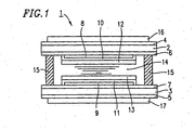
- Figure 1 is a schematic cross-sectional view illustrating a plastic film liquid crystal display device which is produced by using a plastic film liquid crystal display device substrate material according to the present invention.
- component (A) according to the present invention will be described.
- Component (A) is an aliphatic organic compound including at least two carbon-carbon double bonds within one molecule, the at least two carbon-carbon double bonds having reactivity with an SiH group.
- the organic skeleton is preferably a skeleton only containing C, H, N, O, S, and a halogen as component elements thereof.
- an organic skeleton containing a siloxane unit (Si-O-Si) e.g., a polysiloxane-organic block copolymer or a polysiloxane-organic graft copolymer
- Si-O-Si siloxane unit
- the gas permeability is likely to be increased, thus resulting in the deterioration of the liquid crystal material due to permeation of steam or oxygen, or the so-called "repellence" problem may occur, i.e., when a surface coating is performed, the contact angle of the coating material may be increased so that the coating material is repelled to prevent thin film coating.
- component (A) When the structure of component (A) is represented as a skeletal portion and a group (alkenyl group) which is bound to the skeleton via a covalent bond (and optionally via a divalent or higher substituent) and which includes carbon-carbon double bonds having reactivity with an SiH group, the alkenyl group may be present anywhere within the molecule.
- skeleton of component (A) which is an organic compound
- component (A) there is no particular limitation so long as it is aliphatic.
- An organic polymeric skeleton or an organic monomeric skeleton may be used.
- "aliphatic” is used in the sense of excluding aromatic organic compounds, and thus encompasses alicyclic compounds as well.
- organic polymeric skeletons include polyether-base, polyester-base, polyarylate-base, polycarbonate-base, saturated hydrocarbon-base, polyacrylic ester-base, polyamide-base, and polyimide-base skeletons may be used.
- monomeric skeletons include, for example, aliphatic hydrocarbon-base, alicyclic-base, and mixtures thereof.
- alkenyl group in component (A) there is no particular limitation so long as it has reactivity with an SiH group.
- an alkenyl group represented by the following general formula (I): (where R 1 represents a hydrogen atom or a methyl group. in this case, each R 1 may be the same or different) is preferable in terms of reactivity. From the perspective of availability of the material is especially preferable.
- an alkenyl group represented by the following general formula (II). (where R 1 represents a hydrogen atom or a methyl group) is preferable due to the high heat-resistance of the resultant cured substance. From the perspective of availability of the material, is especially preferable.
- the alkenyl group may be covalently bound to the skeletal portion of component (A) via a divalent or higher substituent.
- the divalent or higher substituent there is no particular limitation so long as it is a substituent having 0 to 10 carbons.
- the divalent or higher substituent preferably only contains C, H, N, O, S, and a halogen as component elements thereof, for the same reason that the skeleton of component (A) preferably only contains C, H, N, O, S, and a halogen as component elements thereof.
- substituents include: (where n represents any number from 1 to 10). (where n represents any number from 0 to 4) Two or more of such divalent or higher substituents may be linked via a covalent bond to compose one divalent or higher substituent.
- Examples of groups which are covalently bound to such a skeletal portion include: a vinyl group; an allyl group; a methallyl group; an acryl group; methacryl group; a 2-hydroxy-3-(allyloxy)propyl group; a 2-(allyloxy)ethyl group; a 2,2-bis(allyloxymetbyl)butyl group; a 3-(allyloxy)-2,2-bis(allyloxymethyl)propyl group, and (where n represents a number satisfying 5 ⁇ n ⁇ 2) (where R represents a divalent group selected from (where n represents any number from 0 to 4)
- a low molecular weight compound which is not representable as a skeletal portion and an alkenyl group in the above manner may also be used.
- specific examples of such low molecular weight compounds include: aliphatic chain polyene compounds such as butadiene, isoprene, octadiene. and decadiene; alicyclic polyene compounds such as cyclopentadiene, cyclooctadtene, dicyclopentadiene, tricyclopentadlene, and norbornadiene; substituted alicyclic olefin compounds such as vinylcyclppentene and vinylcyclohexene: and alicyclic compounds such as 1,2,4-trivinylcyclohexane.
- ⁇ , ⁇ -diene compounds such as decadiene are not preferable because they are likely to result in brittle cured substances with inferior mechanical properties.
- an "internal olefin structure” refers to the structure: where one or both of R 1 and R 2 are substituents which are not hydrogen atoms and one or both of R 3 and R 4 are substituents which are nothydrogen atoms.
- component (A) those containing carbon-carbon double bonds haying reactivity with an SiH group in an amount equal to or greater than 0.001 mol per gram of component (A) may be used in order to provide further improved heat-resistance. Those containing the same in an amount equal to or greater than 0.005 mol per gram of component (A) are preferable, and those containing the same in an amount equal to or greater than 0.008 mol per gram of component (A) are especially preferable.
- Specific examples include: butadiene, isoprene, vinylcyclohexene, cyclopentadiene, dicyclopentadiene, cyclohexadiene, decadiene, diallylphthalate, trimethylolpropanediallylether. pentaerythritoltriallylether, and oligomers thereof, 1,2-polybutadiene (with a 1,2 ratio of 10 to 100%, and preferably 50 to 100%), (where R represents a divalent group selected from , and the like.
- the number of carbon-carbon double bonds having reactivity with an SiH group included in component (A) is at least two per molecule. In order to provide further improved heat-resistance, the number is preferably more than two, and more preferably three or more, and especially preferably four or more. In the case where the number of carbon-carbon double bonds having reactivity with an SiH group included in component (A) per molecule of component (A) is equal to or less than one per molecule, only a graft structure results through reaction with component (B), without achieving a cross-linked structure.
- component (A) those having fluidity at a temperature of 100°C or less are preferable in order to obtain homogeneous mixing with other components and good workability.
- Component (A) may be linear or branched. Although there is no particular limitation as to the molecular weight, any value from 50 to 100,000 can be suitably used. If the molecular weight exceeds 100,000, the material generally exhibits a high viscosity, thus detracting from workability, and the effects of cross-linking due to reaction between the alkenyl group and the SiH group become difficult to be exhibited.
- component (B) preferably at least one, and more preferably at least two, of the carbon-carbon double bonds having reactivity with an SiH group which are included in the organic compound which is component (A) are vinyl groups.
- component (B) preferably at least one, and more preferably at least two, of the carbon-carbon double bonds having reactivity with an SiH group which are included in the organic compound which is component (A) are allyl groups.
- preferable component (A) examples include 1,2-polybutadiene, hydrogenated bisphenol A diallylether, 4-vinylcyclohexene, cyclopentadiene, or 1,2,4-trivinylcyclohexane.
- component (B) which is a silicon compound having at least two SiH groups in one molecule, will be described.
- chain and/or cyclic polyorganosiloxanes including at least two SiH groups within one molecule are preferable in terms of availability.
- cyclic polyorganosiloxanes including at least two SiH groups within one molecule which can be represented by the following general formula (III): (where R 2 represents an organic group having 1 to 6 carbons; and n represents any number from 3 to 10) are more preferable.
- the substituent R 2 in the compound which can be represented by general formula (III) is preferably a substituent which is composed of C, H, and O, and more preferably a hydrocarbon group.
- component (B) is preferably a reaction product between a chain and/or cyclic polyorganosiloxane including at least two SiH groups within one molecule (hereinafter referred to as component (D)) and one or more kinds of compounds selected from the group consisting of organic compounds including carbon-carbon double bonds (hereinafter referred to as component (E)).
- component (D) a chain and/or cyclic polyorganosiloxane including at least two SiH groups within one molecule
- component (E) one or more kinds of compounds selected from the group consisting of organic compounds including carbon-carbon double bonds
- component (E) examples include allylether of novolac phenol and bisphenol A diallylether, 2,2'-diallylbisphenol A, diallylphthalate, bis(2-allyloxyethyl)ester of phthalic acid, styrene, ⁇ -methylstyrene, and the like because they can enhance the compatibility of component (B) with component (A).
- component (E) One kind or a mixture of two or more kinds may be used as the organic compound of component (E).
- component (B) described above can be used alone or they may be used as a mixture of two more kinds.
- the mixing ratio between component (A) and component (B) is not particularly limited so long as the necessary strength is not lost. However, it is generally preferable that a ratio between the number of mols (X) representing the number of carbon-carbon double bonds having reactivity with an SiH group in component (A) and the number of mols (Y) representing the number SiH groups in component (B) is 2 ⁇ Y/X ⁇ 0.5. If Y/X > 2 or 0.5 > Y/X, sufficient curing properties cannot be obtained, so that sufficient strength may not be obtained and poor heat-resistance may result.
- the hydrosilylation catalyst there is no particular limitation so long as catalytic activity is obtained.
- catalysts other than. platinum compounds include RhCl(PPh) 3 , RhCl 3 , RhAl 2 O 3 , RuCl 3 , IrCl 3 , FeCl 3 , AlCl 3 , PdCl 2 ⁇ 2H 2 O, NiCl 2 , TiCl 4 , and the like.
- platinic chloride a platinum-olefin complex, a platinum-vinylsiloxane complex and the like are preferable from the perspective of catalytic activity.
- a catalyst may be used alone or two or more kinds may be used together.
- the amount of catalyst to be added there is no particular limitation as to the amount of catalyst to be added.
- a range of 10 -1 to 10 -8 mols per mol of an SiH group is preferable, and a range of 10 -2 to 10 -6 mols is more preferable.
- auxiliary catalyst can be used together with the aforementioned catalyst.
- phosphorous compounds such as triphenylphosphine; 1,2-diester compounds such as dimethylmaleate; acetylene alcohol compounds such as 2-hydroxy-2-methyl-1-butyne; sulfur compounds such as sulfur alone; and amine compounds such as triethylamine.
- amount of auxiliary catalyst to be added a range of 10 -2 to 10 2 mols per mol of the catalyst is preferable, and a range of 10 -1 to 10 mols is more preferable.
- a curing retarder In order to further improve the storage stability of the curable composition of the present invention, or adjust the reactivity of the hydrosilylation reaction during the manufacture process, a curing retarder can be used.
- curing retarders include compounds containing aliphatic unsaturated bonds, organic phosphorous compounds, organic sulfur compounds, nitrogen-containing compounds, tin compounds, organic peroxides and the like, which may be used in combination.
- compounds containing aliphatic unsaturated bonds include propargyl alcohols, en-in compounds, maleates, and the like.
- organic phosphorous compounds include triorganophosphines, diorganophosphines, organophosphones, triorganophosphites, and the like.
- organic sulfur compounds include organomercaptans, diorganosulfides, hydrogen sulfide, benzothiazol, benzothiazoldisulfide, and the like.
- nitrogen-containing compounds include ammonia, primary to tertiary alkylamines, arylamines, urea, hydrazine, and the like.
- tin compounds include halogenated tin (II) dihydrate, tin (II) carboxylate, and the like.
- organic peroxides include di-t-butylperoxide, dicumylperoxide, benzoylperoxide, t-butyl perbenzoate, and the like.
- benzothiazol, thiazol, dimethylmaleate, and 3-hydroxy-3-methyl-1-butyne are preferable because of their good retardation activity and good availability of these materials.
- the amount of a storage stability enhancer to be added is preferably in the range of 10 -1 to 10 3 mols per mol of the hydrosilylation catalyst to be used, and more preferably the range of 1 to 50 mols.
- composition of the present invention various combinations can be used as described above. However, for good heat-resistance, those compositions which are cured to give a cured substance whose Tg is 50°C or more are preferable; those compositions which are cured to give a cured substance whose Tg is 100°C or more are more preferable; and those compositions which are cured to give a cured substance whose Tg is 150°C or more are especially preferable.
- An inorganic filler may be added to the composition of the present invention as necessary.
- the addition of an inorganic filler is effective for preventing the composition from having fluidity, and for strengthening the material.
- the inorganic filler those which are fine particles are preferable so as not to deteriorate the optical characteristics, examples thereof including: alumina, aluminum hydroxide, molten silica, crystalline silica, superfine powder amorphous silica, hydrophobic superfine powder silica, talc, barium sulfate, and the like.
- resins can be added in order to reform the characteristics of the composition according to the present invention.
- resins for example, polycarbonate resin, polyethersulf one resin, polyarylate resin, epoxy resin, cyanate resin, phenol resin, acrylic resin, polyimide resin, polyvinyl acetal resin, urethane resin, and polyester resin may be used; however the resins are not limited thereto.
- anti-aging agents radical inhibitors, ultraviolet absorbents, adhesion modifiers, flame retardants, surfactants, storage stability enhancers, ozone degradation preventing agents, photostabilizers, thickeners, plasticizers, coupling agents, antioxidants, thermostabilizers, conductivity conferrers, antistatic agents, radiation shield agents, nucleating agents, phosphorous-base peroxide decomposers, slip additives, pigments, metal deactivators, physicochemical property adjusters, and the like may be added to the composition according to the present invention to an extent where the purposes and effects of the present invention are not undermined.
- the curable composition according to the present invention can be made into an optical material by being previously mixed so as to allow the carbon-carbon double bonds having reactivity with an SiH group to react with some or all of the SiH groups in the composition, thereby causing curing.
- composition When the composition is allowed to react and cure, necessary amounts of components (A), (B), and (C) may be allowed to react by being mixed at one time. Alternatively, a method may be adopted in which some of these are mixed and allowed to react, and thereafter the remainders are mixed for further reaction. Alternatively, a method may be adopted in which only some of the functional groups within the composition are allowed to react (to enter a "B stage") by controlling the reaction conditions after mixing or utilizing differences in reactivity between the respective functional groups (in the case where a compound which contains functional groups having a relatively high reactivity and functional groups having a relatively low reactivity is used), and thereafter performing a process such as molding for further curing. According to these methods, viscosity adjustment at the time of molding can be facilitated.
- various methods can be adopted as a mixing method, but methods in which component (B) is admixed to a mixture resulting from admixing component (C) to component (A) are preferable.
- alteration in quality may occur during storage because component (B) has reactivity with water in the presence of component (C).
- the reaction may be effected by simple mixing, or the reaction maybe effected by heating.
- a method which involves reaction by heating is preferable because it provides for a quick reaction and a material having a high heat-resistance is generally likely to be obtained.
- the reaction temperature can be set to be various values. For example, a temperature in the range of 30 to 300°C can be used; 100 to 250°C is more preferable; and 150 to 200°C is still more preferable. If the reaction temperature is lower, the reaction time required for causing sufficient reaction becomes long. If the reaction temperature is higher, the molding process is likely to become difficult.
- the reaction may be performed at a constant temperature, but the temperature may be changed in multiple levels or continuously.
- the reaction time may also be set to be various values.
- the pressure during the reaction can also be set to be various values.
- the reaction may be effected at ordinary pressure, high pressure or reduced pressure.
- the optical material which is obtained by curing can also take various shapes depending on the application, and there is no limitation as to the shape.
- a film, sheet, tube, rod, coating film, or bulk shape may be used.
- molding methods various methods may be adopted such as conventional molding methods for thermosetting resins.
- molding methods such as a cast method, a press method, a casting method, a transfer molding method, a coating method, an RIM method, and the like may be adopted.
- a molding die polished glass, a polished hard-stainless steel plate, a polycarbonate plate, a polyethyleneterephthalate plate, a polymethylmethacrylate plate, or the like may be used.
- a polyethyleneterephthalate film a polycarbonate film, a polyvinylchloride film, a polyethylene film, a polytetrafluoroethylene film, a polypropylene film, a polyimide film, or the like may be used.
- a process of degassing a composition or a partially-reacted composition by centrifugation or decompression, a process of temporarily releasing pressure during pressing, or the like may be used in order to control the voids which are generated during molding.
- the composition of the present invention may itself be molded into a film or the like, but it is also possible to dissolve the composition in an organic solvent and use this as a varnish.
- the solvent to be used is not particularly limited.
- hydrocarbon-base solvents such as benzene, toluene, hexane, or heptane
- ether-base solvents such as tetrahydrofuran, 1,4-dioxane, or diethylether
- ketone-base solvents such as acetone or methylethylketone
- halogen-base solvents such as chloroform, methylene chloride, 1,2-dichloroethane can be suitably used.
- Solvents may be used in the form of mixed solvents of two or more kinds.
- a solvent toluene, tetrahydrofurane, or chloroform is preferable.
- the amount of solvent to be used is preferably in the range of 0.001 to 10 mL, more preferably in the range of 0.5 to 5 mL, and especially preferably in the range of 1 to 3 mL per gram of reactive component (A) used. If the amount used is smaller, the effects of using a solvent, such as reduced viscosity, may become difficult to obtained. If the amount used is greater, the solvent may remain in the material to cause problems such as thermal cracks, and cost-wise disadvantages may detract from the industrial value.
- composition according to the present invention can be made into an optical material by being previously mixed so as to allow the carbon-carbon double bonds having reactivity with an SiH group to react with some or all of the SiH groups in the composition, thereby causing curing.
- the curable composition according to the present invention can be used as a composition for an optical material.
- optical materials refer to general materials which are used so as to allow light, such as visible light, infrared light. ultraviolet light, X-rays, or laser light, to pass therethrough.
- liquid crystal display device peripheral materials such as substrate materials, light guide plates, prism sheets, deflection plates, phase-difference plates, viewing-angle correction films, adhesives, and films for use with liquid crystal, e.g., polarizer protection films, are included.
- PLC plasma address liquid crystal
- FED field emission display
- VDs video disks
- CD/CD-ROMs CD-R/RWs
- DVD-R/DVD-RAMs DVD-R/DVD-RAMs
- MO/MDs MO/MDs
- PDs phase change disks
- optical cards are included.
- lens materials, finder prisms, target prisms, finder covers, and photosensitive sensors for still picture cameras; and imaging lenses and finders for video cameras are included.
- projection lenses, protection films, sealants, adhesives, and the like for projection televisions are included.
- Lens materials, sealants, adhesives, films, and the like for optical sensing devices are included.
- fiber materials, lenses, waveguides, sealants for elements, adhesives, and the like associated with optical switches in an optical communication system are included.
- Optical fibers, ferrules, sealants, adhesives, and the like associated with optical connectors are included.
- Lenses, waveguides, sealants for LED devices, adhesives, and the like for optical passive components, and optical circuit components are included.
- Substrate materials, fiber materials, sealants for elements, adhesives, and the like associated with optical electric integrated circuits (OEICs) are included.
- illuminations for ornamental displays, light guides, and the like are included.
- sensors for industrial use are included.
- displays, signs, and the like are included.
- resist materials for microlithography for LSIs or VLSIs are included.
- lamp reflectors In the field of automobiles and transport vehicles, lamp reflectors, bearing retainers, gear portions. resist coats, switch portions, headlamps, engine internal components, electronic components, various interior and exterior components, driving engines, break oil tanks, automobile rust-proof steel plates, interior panels, interior materials, wirenesses for protection and binding purposes, fuel hoses, automobile lamps, and alternative materials to glass for automobiles are included. Moreover, multi-layer glass for railroad vehicles are included. Moreover, toughness conferrers, engine peripheral members, wirenesses for protection and binding purposes, and resist coats for structural materials of aircraft are included.
- organic EL element peripheral materials In the field of architecture, interior, processing materials, electric covers, sheets, glass intermediate films, alternative materials to glass, and solar battery peripheral materials are included. As for agricultural use, house-covering films are included.
- organic EL element peripheral materials As for next-generation photo/electronic function organic materials, organic EL element peripheral materials, substrate materials, fiber materials, sealants for elements, adhesives and the like associated with organic photorefractive elements, optical amplifier elements as light-to-light conversion devices, optical mathematical operation elements, as well as organic solar batteries.
- a liquid crystal display device can be produced by employing the aforementioned optical material.
- a liquid crystal display device may be produced by usual methods.
- the transparent conductive film according to the present invention is a film comprising a transparent conductive layer provided on at least one face of a transparent film composed of a curable composition including the aforementioned components (A) to (C) as essential components.
- a curable composition including the aforementioned components (A) to (C) as essential components.
- the transparent conductive layer according to the present invention is produced by coating a transparent conductive film such as a thin metal film, a thin semiconductor film, or a thin multilayer film on at least one face of a transparent film; there is no particular limitation with respect to all surface or one face, etc.
- Examples of thin metal films include nickel, titanium, chromium, silver, zinc, aluminum, copper, gold, palladium, and the like.
- Examples of thin semiconductor films include metal oxide films, such as indium oxide, cadmium oxide, and tin oxide to which tin, tellurium, cadmium, molybdenum, tungsten, fluorine, or the like is added as an impurity; and zinc oxide, titanium oxide and the like to which aluminum is added as an impurity.
- thin semiconductor films of indium tin oxide (ITO) containing 2 to 15 wt% of tin oxide are excellent in conductivity and are preferably used.
- Examples of thin multilayer films composed of dielectric/metal/dielectric include titanium oxide/gold/titanium oxide and the like.
- the thickness of the transparent conductive film is preferably 5 to 200 nm. If the thickness of the transparent conductive film is less than 5 nm, it may be difficult to form the film. If the thickness of the transparent conductive film exceeds 200 nm, transparency may be lowered, and bending resistance may be deteriorated.
- Examples of methods for forming such transparent conductive films include a vacuum deposition method, a sputtering method, an ion plating method, ion beam sputtering method, and the like.
- thermosetting resins As methods for producing transparent films as substrates for transparent conductive films, various methods can be adopted, including conventional molding methods for thermosetting resins.
- a polyethyleneterephthalate film, a polycarbonate film, a polyvinylchloride film, a polyethylene film, a polytetrafluoroethylene film, a polypropylene film, a polyimide film, or the like may be used.
- a thin film may be applied in order to confer functions such as gas barrier property, anti-abrasion property, chemical resistance, and the like.
- thermoplastic resins thermosetting resins containing amino groups, imino groups, epoxy groups, silyl groups, and the like; radiation curing resins containing acryloyl groups, methacryloyl groups, vinyl groups, and the like; or mixtures of these resins, to which polymerization inhibitors, waxes, dispersants, pigments, solvents, dyes, plasticizers, ultraviolet absorbents, inorganic fillers, and the like are added, may be applied by methods such as a gravure roll coating method, a Mayer bar coating method, a reverse roll coating method, a dip coating method, an air knife coating method, a calender coating method, a squeeze coating method, a kiss coating method, a fountain coating method, a spray coating method, a spin coating method, and the like.
- curing via radiation irradiation or thermal curing via heating may be performed as necessary to obtain a cured thin film layer.
- methods such as a gravure method, an offset method, a flexography method, a silkscreen method, and the like can be used.
- a metal oxide layer containing aluminum, silicon, magnesium, zinc, and the like as main components may be provided, where the metal oxide layer is formed by a vacuum deposition method, a sputtering method, an ion plating method, or a plasma CVD method.
- any known and commonly-used method may be used, e.g., thermal bonding methods such as a heat sealing method, an impulse sealing method, an ultrasonic bonding method, a high-frequency bonding method; laminate processing methods such as an extrusion lamination method, a hot-melt lamination method, a dry lamination method, a wet lamination method, a solvent-free adhesion lamination method, a thermal lamination method, and a coextrusion method; and the like.
- thermal bonding methods such as a heat sealing method, an impulse sealing method, an ultrasonic bonding method, a high-frequency bonding method
- laminate processing methods such as an extrusion lamination method, a hot-melt lamination method, a dry lamination method, a wet lamination method, a solvent-free adhesion lamination method, a thermal lamination method, and a coextrusion method; and the like.
- films to be used for lamination examples include a polyester resin film, a polyvinyl alcohol resin film, a cellulose resin film, a polyvinylfluoride resin film, a polyvinylidene chloride resin film, polyacrylonitrile resin film, a nylon resin film, a polyethylene resin film, a polypropylene resin film, an acetate resin film, a polyimide resin film, a polycarbonate film, a polyacrylate film, and the like.
- Examples of applications of the transparent film according to the present invention include the following:
- a stirring apparatus and a condenser were set to a 1 L three-necked flask.
- 114 g of bisphenol A, 145 g of potassium carbonate, 140 g of allylbromide, and 250 mL of acetone were placed, and this was stirred for 12 hours at 60°C.
- a supernatant was taken, and washed with an aqueous solution of sodium hydroxide in a separatory funnel, and thereafter washed with water.
- the organic layer was dried with sodium sulfate, the solvent was distilled away by means of an evaporator, whereby 126 g of a pale yellow liquid was obtained.
- this was found to be bisphenol A diallylether, i.e., bisphenol A having an OH group thereof allyletherified.
- the yield was 82% and the purity was 95% or more.
- a stirring apparatus, a condenser, and a dropping funnel were set to a 1 L four-necked flask.
- 150 g of toluene, 15.6 ⁇ L of a xylene solution of a platinum-vinylsiloxane complex (containing 3 wt% of platinum), 500 g of 1,3,5,7-tetramethylcyclotetrasiloxane were added, and this was heated to 70°C and stirred in an oil bath.
- Sixty-four grams of bisphenol A diallylether produced according to Example 1 was diluted with 40 g of toluene, and added dropwise through the dropping funnel.
- a stirring apparatus and a condenser were set to a 500 mL four-necked flask.
- this flask 6.49 g of hydrogenatedbisphenol A (manufactured by Tokyo Kasel Co., Ltd.) represented by the following formula: 243 g of a 50 wt% aqueous solution of sodium hydroxide, 3.54 g of tetra n-butyl ammonium bromide, 20.5 g of allylchloride, and 16.0 mL of xylene were placed, and this was heated and stirred for 5 hours at 60°C, and then 4 hours at 70°C in nitrogen. The organic layer was separated through a separatory funnel.
- this composition was cast on a PET film as a release film so as to have a thickness of 0.2 mm by using a bar coater. In a nitrogen atmosphere, this was heated so as to cure for 30 minutes at 100°C, and then 15 hours at 120°C. A film was obtained which proved homogeneous and transparent by visual inspection.
- this composition was cast on a PET film as a release film so as to have a thickness of 0.2 mm by using a bar coater. In a nitrogen atmosphere, this was heated so as to cure for 30 minutes at 100°C, and then 15 hours at 120°C. A film was obtained which proved homogeneous and transparent by visual inspection.
- the plastic film liquid crystal display device substrate material according to the present invention has excellent properties of low birefringence and high total ray transmittance as compared to polycarbonate films.
- a liquid crystal display device having a high display quality can be produced.
- Example 1 After being degassed for 1 hour under a reduced pressure of about 1 torr, the same composition as that of Example 1 was press-molded with a pressure of 3 kg/cm 2 for 1 hour at 150°C, by using a crystallized PET film as a release film and using 0.3 mm-thick silicone rubber as a spacer.
- the material thus obtained had characteristics similar to those of the material obtained according to Example 1.
- Example 2 After being degassed for 1 hour under a reduced pressure of about 1 torr, the same composition as that of Example 1 was cast by using a bar coater and using a PET film as a release film. This was heated so as to cure for 30 minutes at 100°C, and then 15 hours at 120°C. A film having a thickness of 180 ⁇ m, which proved homogeneous and transparent by visual inspection, was obtained.
- an indium tin oxide (ITO) film was formed as a transparent conductive layer by using a sputtering method as follows.
- Shimadzu Sputtering System HSM-421 was used as a sputtering apparatus, and indium tin oxide containing 90 wt% of indium oxide and 10 wt% of tin oxide was used as a target.
- the transparent film as set in the sputtering apparatus the sputtering apparatus was deaired down to a pressure of 2.1 ⁇ 10 -5 Torr at room temperature. Next, argon was introduced and sputtering was performed, whereby a transparent conductive film having a thickness of 100 nm was formed, with a surface resistance of 119 ⁇ / ⁇ .
- the sputtering apparatus was deaired down to a pressure of 3.6 ⁇ 10 -5 Torr at a temperature of 250°C.
- argon was introduced and sputtering was performed, whereby a transparent conductive film having a thickness of 100 nm was formed, with a surface resistance of 69 ⁇ / ⁇ .
- the liquid crystal display device according to the present invention may be as follows, for example.
- Figure 1 is a cross-sectional view illustrating the structure of a plastic film liquid crystal display device 1 which can be produced employing the plastic film liquid crystal display device substrate material according to the present invention.
- the liquid crystal display device 1 includes a pair of transparent substrates 2 and 3 which have translucency.
- gas barrier layers 4 and 5 for preventing the entry of gases, such as oxygen or steam, into the liquid crystal layer are formed.
- the gas barrier layers 4 and 5 which may be optionally formed in the case where a higher level of anti-gas permeability is required depending on the environment used, are formed of polyvinylalcohol or the like.
- undercoat layers 6 and 7 of vapor-deposited SiO x having a thickness of 150 to 1000 ⁇ are formed on the opposing surfaces of the transparent substrates 2 and 3 .
- transparent conductive films 8 and 9 of ITO (indium tin oxide) are sputter deposited so as to have a thickness of about 1500 ⁇ .
- topcoat layers 10 and 11 and alignment films 12 and 13 of polyimide are spin coated or printed so as to have a thickness of about 500 ⁇ .
- a liquid crystal material 14 is injected and sealed with a sealing member 15 .
- polarizing plates 16 and 17 are layered. The liquid crystal display device 1 is thus constructed.
- the plastic film liquid crystal display device substrate material according to the present invention has only a small retardation, the liquid crystal display device has an improved display quality.
- a curable composition having a high heat-resistance, a low birefringence, a small coefficient of photoelasticity; a high optical transparency, and toughness can be provided.
- an optical material having a high optical transparency and toughness By employing this curable composition, an optical material having a high optical transparency and toughness, a method for producing the same, and a liquid crystal display device incorporating the same can be provided.
- a transparent conductive film having excellent optical characteristics can be provided.
Landscapes
- Physics & Mathematics (AREA)
- Chemical & Material Sciences (AREA)
- Nonlinear Science (AREA)
- General Physics & Mathematics (AREA)
- Optics & Photonics (AREA)
- Crystallography & Structural Chemistry (AREA)
- Mathematical Physics (AREA)
- Polymers & Plastics (AREA)
- Organic Chemistry (AREA)
- Health & Medical Sciences (AREA)
- Medicinal Chemistry (AREA)
- Chemical Kinetics & Catalysis (AREA)
- Compositions Of Macromolecular Compounds (AREA)
- Liquid Crystal (AREA)
- Silicon Polymers (AREA)
- Laminated Bodies (AREA)
Abstract
A curable composition comprising: component (A),
which is an aliphatic organic compound including at least
two carbon-carbon double bonds within one molecule, the
at least two carbon-carbon double bonds having reactivity
with an SiH group; component (B), which is a compound
including at least two SiH groups within one molecule;
and component (C), which is a hydrosilylation catalyst.
The curable composition can be made into an optical material
by being previously mixed so as to allow the carbon-carbon
double bonds having reactivity with an SiH group to react
with some or all of the SiH groups in the composition,
thereby causing curing. There is provided a curable
composition having a high heat-resistance, a low
birefringence, a small coefficient of photoelasticity,
a high optical transparency, and toughness; an optical
material; a method for producing the same; and a liquid
crystal display device incorporating the same.
Description
The present invention relates to a curable
composition, and in particular to a curable composition
from which an optical material having high heat-resistance,
high optical transparency, and toughness can be obtained.
By using the curable composition according to the
present invention, various optical materials can be
produced, e.g., members to be used in liquid crystal display
devices; transparent conductive films to be suitably used
as input devices for portable information terminals, car
navigation systems, and the like; and plastic film liquid
crystal display devices to be suitably used as displays
for mobile phones, portable information terminals,
personal computers, and the like, which are strongly
desired to become lighter in weight and thinner in size.
As optical materials such as those for liquid
crystal display devices, materials which have a low
birefringence, a small coefficient of photoelasticity,
and a high optical transparency are used. In the case
of materials for liquid crystal display devices and the
like, any materials used therein are required to have a
high heat-resistance from the perspective of the
manufacturing process. Glass and the like have
conventionally been used as materials satisfying such
requirements.
Optical materials such as those for liquid crystal
display devices are generally used in the form of thin
films or thin tubes or rods. Recent market requirements
have called for the use of even thinner films and thinner
tubes or rods. However, since the conventionally-used
glass is brittle in terms of strength, it can only be used
for a limited scope of use.
One example of materials having toughness is
polymer materials. However, in the case of a thermoplastic
resin, for example, introducing an aromatic skeleton into
its molecule for allowing a high heat-resistance to be
exhibited generally results in a high birefringence and
a large coefficient of photoelasticity, thus making the
reconciliation of high heat-resistance and optical
characteristics difficult. As for thermosetting resins,
conventionally known thermosetting resins are generally
colored and therefore not suitable for optical material
applications. Furthermore, thermosetting resins are
generally polarized, which is disadvantageous for the
exhibition of optical performance.
Transparent conductive films are plastic films which
are transparent and conductive, and are functional films
which are utilized in technological fields where light.
and electricity are involved. With recent advancements
in electronics, reduction in weight, size, cost of parts
and devices for which transparent conductive films are
employed are desired, along with increased design
flexibility and higher performance. For both
conventional applications and new applications,
transparent conductive films are expected to have improved
functions.
Transparent conductive films are required to have
a high light transmittance. In applications such as liquid
crystal display and optical recording, optical
characteristics such as birefringence are also regarded
as important. As conventional transparent conductive
films, those based on a substrate of polyester (hereinafter
abbreviated as "PET") films or polycarbonate (hereinafter
abbreviated as "PC") films, with a thin metal film or a
thin semiconductor film such as ITO formed on the surface
thereof, are known.
A transparent conductive film whose substrate is
a PET film has a large optical anisotropy because the PET
film has a molecular orientation due to a stretching
operation performed during the. manufacture thereof,
thereby being inferior in birefringence. A transparent
conductive film whose substrate is a PC film exhibits a
large polarization anisotropy because the PC includes a
group having a substantial polarization rate, e.g., a
benzene ring, within its molecule, and therefore is likely
to have birefringence.
Thus, conventional transparent conductive films
have their advantages and disadvantages, and cannot
necessarily be considered as satisfying the higher-level
and more-complicated requirements of the recent years.
In recent years, liquid crystal display devices
have faced some sophisticated requirements, e.g., they
are required to be in a thinner film configuration, lighter
in weight, larger insize, shaped arbitrarily, and capable
of displaying on a curved surface. In particular, in
answer to the expanded use of devices which are carried
on one's body, e.g., mobile phones, electronic organizers,
and pen input devices, liquid crystal display panels
employing plastic substrates, as opposed to
conventionally-employed glass substrates, have been
contemplated and partly begun to be put to practical use.
For example, polyethersulfone (hereinafter abbreviated
as "PES") and polycarbonate (PC) film substrates, which
do not exhibit optical anisotropy, are available.
Plastic film substrates need to satisfy
requirements such as capability to lose optical anisotropy.
heat-resistance, solvent-resistance, gas barrier
property, surface flatness, geometrical stability, and
translucency. The aforementioned PES exhibits an
increased substrate retardation when formed with a
thickness of 0.1 mm or above. An increased substrate
retardation leads to an increased retardation of the entire
liquid crystal display device, a coloration phenomenon,
and the like, thus unfavorably affecting the display
quality of the liquid crystal display device. Since PES
has a heat-resistance of up to 150°C, the component
materials of a liquid crystal display device must be
subjected to low-temperature sintering. The
aforementioned PC also exhibits an increased substrate
retardation when formed with a thickness of 0.1 mm or above,
resulting in problems similar to those associated with
PES.
In order to solve the aforementioned problems, the
inventors conducted vigorous research to find that the
aforementioned problems can be solved by employing a
curable composition comprising as essential components:
an organic compound including at least two carbon-carbon
double bonds within one molecule, the at least two
carbon-carbon double bonds having reactivity with an
SiH group; and a silicon compound including at least two
SiH groups within one molecule, thereby arriving at the
present invention.
Specifically, a curable composition according to
the present invention comprises: component (A), which is
an aliphatic organic compound including at least two
carbon-carbon double bonds within one molecule, the at
least two carbon-carbon double bonds having reactivity
with an SiH group; component (B), which is a compound
including at least two SiH groups within one molecule;
and component (C), which is a hydrosilylation catalyst.
In one embodiment, at least one of the
carbon-carbon double bonds included in component (A) is
a vinyl group or an allyl group.
In one embodiment, component (A) is
1,2-polybutadiene, hydrogenated bisphenol A diallylether,
4-vinylcyclohexene, or 1,2,4-trivinylcyclohexane.
A composition for an optical material according
to the present invention employs the aforementioned
curable composition.
In one embodiment, the optical material is a film
for use with liquid crystal.
In one embodiment, the optical material is a
plastic cell for use with liquid crystal.
An optical material according to the present
invention is obtained by mixing the aforementioned curable
composition so as to allow the carbon-carbon double bonds
included in component (A) to react with some or all of
the SiH groups included in component (B), thereby causing
curing.
A method for producing an optical material
according to the present invention comprises the steps
of: mixing the aforementioned composition for an optical
material; and allowing the carbon-carbon double bonds
included in component (A) to react with some or all of
the SiH groups included in component (B).
A liquid crystal display device according to the
present invention incorporates the aforementioned optical
material.
A transparent conductive film according to the
present invention comprises a transparent film composed
of the cured aforementioned curable composition, and a
transparent conductive layer provided on at least one
surface of the transparent film.
A method for producing a transparent conductive
film according to the present invention comprises
producing the aforementioned transparent conductive film
with a molding die.
In one embodiment, the molding die is made of glass
whose surface is polished.
In one embodiment, the molding die comprises a
polished hard-stainless steel plate.
In one embodiment, the method comprises producing
the transparent conductive film by a solution flow method.
A plastic film liquid crystal display device
according to the present invention comprises a liquid
crystal layer interposed between a pair of plastic film
substrates, wherein one or both of the substrates are
obtained by curing the aforementioned curable composition.
In one embodiment, the liquid crystal display layer
is of a super twisted nematic type.
In one embodiment, the substrates used for the
liquid crystal display device are produced with a molding
die.
In one embodiment, the molding die is made of glass
whose surface is polished.
In one embodiment, the molding die comprises a
polished hard-stainless steel plate.
In one embodiment, the method comprises producing
the plastic film substrates used for the liquid crystal
display device by a solution flow method.
Materials which are produced from the composition
of the present invention have low birefringence and high
optical transparency as well as toughness, and therefore
are suitable as optical materials.
Since transparent conductive films which are
produced from the composition of the present invention
have low retardation and high optical transparency, they
can be used for applications requiring sophisticated and
complicated properties as in the electronics fields.
Plastic film liquid crystal display device
substrate materials which are produced from .the
composition of the present invention have low retardation
and high optical transparency, and therefore are suitable
as plastic film liquid crystal display device substrate
materials.
Figure 1 is a schematic cross-sectional view
illustrating a plastic film liquid crystal display device
which is produced by using a plastic film liquid crystal
display device substrate material according to the present
invention.
Hereinafter, the present invention will be
described in detail.
First, component (A) according to the present
invention will be described.
Component (A) is an aliphatic organic compound
including at least two carbon-carbon double bonds within
one molecule, the at least two carbon-carbon double bonds
having reactivity with an SiH group.
In the case where component (A) has an organic
skeleton, the organic skeleton is preferably a skeleton
only containing C, H, N, O, S, and a halogen as component
elements thereof. In the case where an organic skeleton
containing a siloxane unit (Si-O-Si), e.g., a
polysiloxane-organic block copolymer or a
polysiloxane-organic graft copolymer, is used, the gas
permeability is likely to be increased, thus resulting
in the deterioration of the liquid crystal material due
to permeation of steam or oxygen, or the so-called
"repellence" problem may occur, i.e., when a surface
coating is performed, the contact angle of the coating
material may be increased so that the coating material
is repelled to prevent thin film coating.
When the structure of component (A) is represented
as a skeletal portion and a group (alkenyl group) which
is bound to the skeleton via a covalent bond (and optionally
via a divalent or higher substituent) and which includes
carbon-carbon double bonds having reactivity with an SiH
group, the alkenyl group may be present anywhere within
the molecule.
As the skeleton of component (A), which is an
organic compound, there is no particular limitation so
long as it is aliphatic. An organic polymeric skeleton
or an organic monomeric skeleton may be used. In the
present specification, "aliphatic" is used in the sense
of excluding aromatic organic compounds, and thus
encompasses alicyclic compounds as well.
As examples of organic polymeric skeletons include
polyether-base, polyester-base, polyarylate-base,
polycarbonate-base, saturated hydrocarbon-base,
polyacrylic ester-base, polyamide-base, and
polyimide-base skeletons may be used.
Examples of monomeric skeletons include, for
example, aliphatic hydrocarbon-base, alicyclic-base, and
mixtures thereof.
As for the alkenyl group in component (A), there
is no particular limitation so long as it has reactivity
with an SiH group. However, an alkenyl group represented
by the following general formula (I):
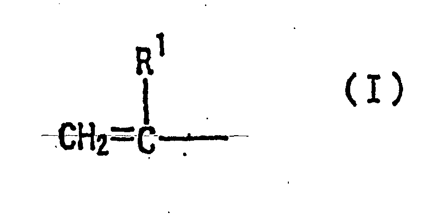 (where R1 represents a hydrogen atom or a methyl group.
in this case, each R1 may be the same or different) is
preferable in terms of reactivity. From the perspective
of availability of the material
(where R1 represents a hydrogen atom or a methyl group.
in this case, each R1 may be the same or different) is
preferable in terms of reactivity. From the perspective
of availability of the material
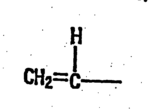 is especially preferable.
As the alkenyl group in component (A), an alkenyl
group represented by the following general formula (II).
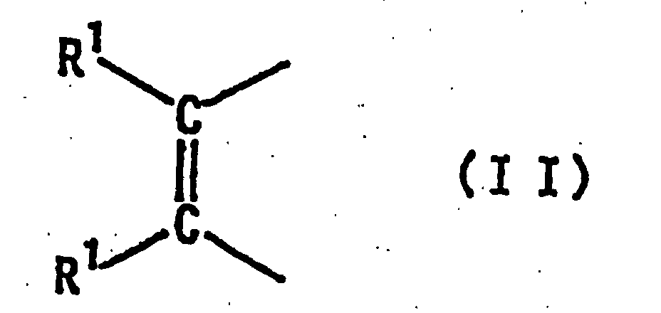 (where R1 represents a hydrogen atom or a methyl group)
is preferable due to the high heat-resistance of the
resultant cured substance. From the perspective of
availability of the material,
(where R1 represents a hydrogen atom or a methyl group)
is preferable due to the high heat-resistance of the
resultant cured substance. From the perspective of
availability of the material,
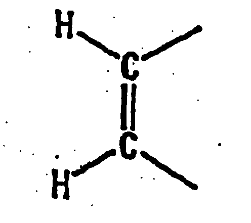 is especially preferable.
The alkenyl group may be covalently bound to the
skeletal portion of component (A) via a divalent or higher
substituent. As the divalent or higher substituent, there
is no particular limitation so long as it is a substituent
having 0 to 10 carbons. However, the divalent or higher
substituent preferably only contains C, H, N, O, S, and
a halogen as component elements thereof, for the same reason
that the skeleton of component (A) preferably only
contains C, H, N, O, S, and a halogen as component elements
thereof. Examples of such substituents include:


 (where n represents any number from 1 to 10).
 (where n represents any number from 0 to 4)
Two or more of such divalent or higher substituents may be linked via a covalent bond to compose one divalent or higher substituent.
Two or more of such divalent or higher substituents may be linked via a covalent bond to compose one divalent or higher substituent.
Examples of groups which are covalently bound to
such a skeletal portion include: a vinyl group; an allyl
group; a methallyl group; an acryl group; methacryl group;
a 2-hydroxy-3-(allyloxy)propyl group; a
2-(allyloxy)ethyl group; a 2,2-bis(allyloxymetbyl)butyl
group; a 3-(allyloxy)-2,2-bis(allyloxymethyl)propyl
group, and
 (where n represents a number satisfying 5≧n≧2)
(where R represents a divalent group selected from
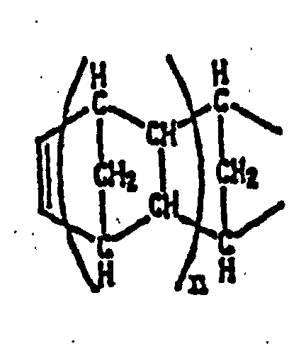 (where n represents any number from 0 to 4)
(where R represents a divalent group selected from
As component (A), a low molecular weight compound
which is not representable as a skeletal portion and an
alkenyl group in the above manner may also be used.
Specific examples of such low molecular weight compounds
include: aliphatic chain polyene compounds such as
butadiene, isoprene, octadiene. and decadiene; alicyclic
polyene compounds such as cyclopentadiene, cyclooctadtene,
dicyclopentadiene, tricyclopentadlene, and
norbornadiene; substituted alicyclic olefin compounds
such as vinylcyclppentene and vinylcyclohexene: and
alicyclic compounds such as 1,2,4-trivinylcyclohexane.
Among these instances of component (A), α,ω-diene
compounds such as decadiene are not preferable because
they are likely to result in brittle cured substances with
inferior mechanical properties.
As component (A), those which do not include an
internal olefin structure are preferable. In the case
where an internal olefin structure is included, the
internal olefin structure is likely to be left unreacted
after hydrosilylation curing reaction, thereby resulting
in poor photo-deterioration properties. As used herein,
an "internal olefin structure" refers to the structure:
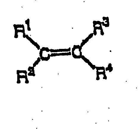 where one or both of R1 and R2 are substituents which are
not hydrogen atoms and one or both of R3 and R4 are
substituents which are nothydrogen atoms.
where one or both of R1 and R2 are substituents which are
not hydrogen atoms and one or both of R3 and R4 are
substituents which are nothydrogen atoms.
As component (A), those containing carbon-carbon
double bonds haying reactivity with an SiH group in an
amount equal to or greater than 0.001 mol per gram of
component (A) may be used in order to provide further
improved heat-resistance. Those containing the same in
an amount equal to or greater than 0.005 mol per gram of
component (A) are preferable, and those containing the
same in an amount equal to or greater than 0.008 mol per
gram of component (A) are especially preferable.
Specific examples include: butadiene, isoprene,
vinylcyclohexene, cyclopentadiene, dicyclopentadiene,
cyclohexadiene, decadiene, diallylphthalate,
trimethylolpropanediallylether.
pentaerythritoltriallylether, and oligomers thereof,
1,2-polybutadiene (with a 1,2 ratio of 10 to 100%, and
preferably 50 to 100%),


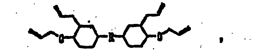
 (where R represents a divalent group selected from

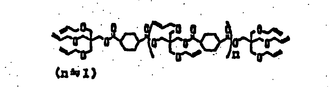 , and the like.
The number of carbon-carbon double bonds having
reactivity with an SiH group included in component (A)
is at least two per molecule. In order to provide further
improved heat-resistance, the number is preferably more
than two, and more preferably three or more, and especially
preferably four or more. In the case where the number
of carbon-carbon double bonds having reactivity with an
SiH group included in component (A) per molecule of
component (A) is equal to or less than one per molecule,
only a graft structure results through reaction with
component (B), without achieving a cross-linked
structure.
As component (A), those having fluidity at a
temperature of 100°C or less are preferable in order to
obtain homogeneous mixing with other components and good
workability. Component (A) may be linear or branched.
Although there is no particular limitation as to the
molecular weight, any value from 50 to 100,000 can be
suitably used. If the molecular weight exceeds 100,000,
the material generally exhibits a high viscosity, thus
detracting from workability, and the effects of
cross-linking due to reaction between the alkenyl group
and the SiH group become difficult to be exhibited.
In order to further enhance the reactivity with
component (B), preferably at least one, and more
preferably at least two, of the carbon-carbon double bonds
having reactivity with an SiH group which are included
in the organic compound which is component (A) are vinyl
groups.
In order to further enhance the reactivity with
component (B), preferably at least one, and more
preferably at least two, of the carbon-carbon double bonds
having reactivity with an SiH group which are included
in the organic compound which is component (A) are allyl
groups.
From the perspective of industrial availability,
specific examples of preferable component (A) include
1,2-polybutadiene, hydrogenated bisphenol A
diallylether, 4-vinylcyclohexene, cyclopentadiene, or
1,2,4-trivinylcyclohexane.
Next, component (B), which is a silicon compound
having at least two SiH groups in one molecule, will be
described.
There is no particular limitation as to the
compound having SiH groups which can be used in the present
invention. For example, a compound as disclosed in
International Laid-Open Publication No. WO96/15194 which
includes at least two SiH groups within one molecule may
be used, among others.
Among these, chain and/or cyclic
polyorganosiloxanes, including at least two SiH groups
within one molecule are preferable in terms of availability.
For good compatibility with component (A), cyclic
polyorganosiloxanes including at least two SiH groups
within one molecule which can be represented by the
following general formula (III):
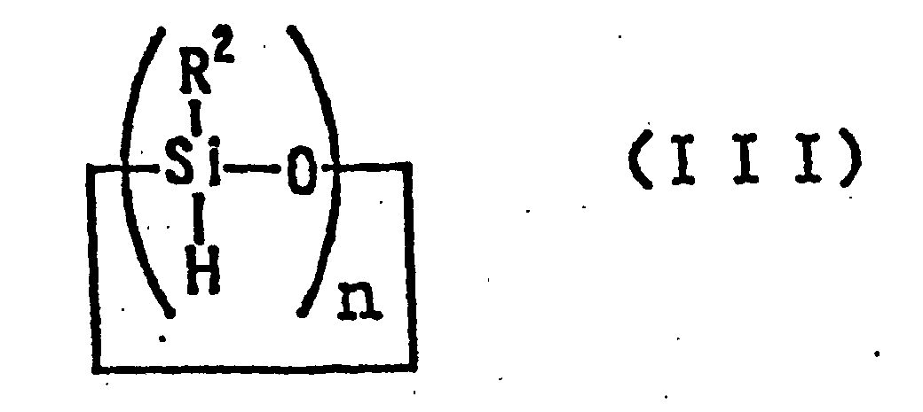 (where R2 represents an organic group having 1 to 6 carbons;
and n represents any number from 3 to 10) are more preferable.
For good industrial availability, the substituent R2 in
the compound which can be represented by general
formula (III) is preferably a substituent which is
composed of C, H, and O, and more preferably a hydrocarbon
group.
(where R2 represents an organic group having 1 to 6 carbons;
and n represents any number from 3 to 10) are more preferable.
For good industrial availability, the substituent R2 in
the compound which can be represented by general
formula (III) is preferably a substituent which is
composed of C, H, and O, and more preferably a hydrocarbon
group.
In order to attain good compatibility with the
aforementioned component (A), component (B) is
preferably a reaction product between a chain and/or cyclic
polyorganosiloxane including at least two SiH groups
within one molecule (hereinafter referred to as
component (D)) and one or more kinds of compounds selected
from the group consisting of organic compounds including
carbon-carbon double bonds (hereinafter referred to as
component (E)). In this case, a compound having an
SiH group (component (B)) can be obtained from
hydrosilylation reaction between excess of component (D)
and a relatively small amount of component (E).
Specific preferable examples of component (E)
include allylether of novolac phenol and bisphenol A
diallylether, 2,2'-diallylbisphenol A, diallylphthalate,
bis(2-allyloxyethyl)ester of phthalic acid, styrene,
α-methylstyrene, and the like because they can enhance
the compatibility of component (B) with component (A).
One kind or a mixture of two or more kinds may be used
as the organic compound of component (E).
Each of various instances of component (B)
described above can be used alone or they may be used as
a mixture of two more kinds.
The mixing ratio between component (A) and
component (B) is not particularly limited so long as the
necessary strength is not lost. However, it is generally
preferable that a ratio between the number of mols (X)
representing the number of carbon-carbon double bonds
having reactivity with an SiH group in component (A) and
the number of mols (Y) representing the number SiH groups
in component (B) is 2 ≧ Y/X ≧ 0.5. If Y/X > 2 or 0.5 >
Y/X, sufficient curing properties cannot be obtained, so
that sufficient strength may not be obtained and poor
heat-resistance may result.
Next, a hydrosilylation catalyst, which is
component (C), will be described.
As for the hydrosilylation catalyst, there is no
particular limitation so long as catalytic activity is
obtained. For example, platinum alone; solid platinum
carried by a carrier such as aluminas, silica, or
carbonblack; platinic chloride; a complex of platinic
chloride and alcohols, aldehydes, ketones, etc.; a
platinum-olefin complex (e.g., Pt(CH2=CH2)2(PPh3)2 or
Pt(CH2=CH2)2Cl2), platinum-vinylsiloxane complex (e.g.,
Pt(ViMe2SiOSiMe2Vi)n, Pt[(MeViSiO)4]m], a
platinum-phosphine complex (e.g., Pt(PPh3)4 or Pt(PBu3)4);
a platinum-phosphite complex (e.g., Pt[P(OPh)3]4 or
Pt[P(OBu)3]4) (where Me represents a methyl group; Bu
represents a butyl group; Vi represents a vinyl group;
Ph represents a phenyl group; and n and m represent
integers); dicarbonyldichloro platinum; Karstedt
catalyst; a platinum-hydrocarbon composite described in
the specifications of USP Nos. 3159601 and 3159662 to
Ashby; and a platinum alcoholate catalyst described in
the specification of USP No. 3220972 to Lamoreaux.
Furthermore, a platinum chloride-olefin composite
described in the specification of USP No. 3516946 to Modic
is also useful in the present invention.
Examples of catalysts. other than. platinum
compounds include RhCl(PPh)3, RhCl3, RhAl2O3, RuCl3, IrCl3,
FeCl3, AlCl3, PdCl2 · 2H2O, NiCl2, TiCl4, and the like.
Among these, platinic chloride, a platinum-olefin
complex, a platinum-vinylsiloxane complex and the like
are preferable from the perspective of catalytic activity.
Such a catalyst may be used alone or two or more kinds
may be used together.
There is no particular limitation as to the amount
of catalyst to be added. However, in order to provide
sufficient curing properties and maintain the cost of the
curable composition relatively low, a range of 10-1 to 10-8
mols per mol of an SiH group is preferable, and a range
of 10-2 to 10-6 mols is more preferable.
An auxiliary catalyst can be used together with
the aforementioned catalyst. For example, phosphorous
compounds such as triphenylphosphine; 1,2-diester
compounds such as dimethylmaleate; acetylene alcohol
compounds such as 2-hydroxy-2-methyl-1-butyne; sulfur
compounds such as sulfur alone; and amine compounds such
as triethylamine. There is no particular limitation as
to the amount of auxiliary catalyst to be added. However,
a range of 10-2 to 102 mols per mol of the catalyst is
preferable, and a range of 10-1 to 10 mols is more preferable.
In order to further improve the storage stability
of the curable composition of the present invention, or
adjust the reactivity of the hydrosilylation reaction
during the manufacture process, a curing retarder can be
used.
Examples of curing retarders include compounds
containing aliphatic unsaturated bonds, organic
phosphorous compounds, organic sulfur compounds,
nitrogen-containing compounds, tin compounds, organic
peroxides and the like, which may be used in combination.
Examples of compounds containing aliphatic unsaturated
bonds include propargyl alcohols, en-in compounds,
maleates, and the like. Examples of organic phosphorous
compounds include triorganophosphines,
diorganophosphines, organophosphones,
triorganophosphites, and the like. Examples of organic
sulfur compounds include organomercaptans,
diorganosulfides, hydrogen sulfide, benzothiazol,
benzothiazoldisulfide, and the like. Examples of
nitrogen-containing compounds include ammonia, primary
to tertiary alkylamines, arylamines, urea, hydrazine, and
the like. Examples of tin compounds include halogenated
tin (II) dihydrate, tin (II) carboxylate, and the like.
Examples of organic peroxides include di-t-butylperoxide,
dicumylperoxide, benzoylperoxide, t-butyl perbenzoate,
and the like.
Among these curing retarders, benzothiazol,
thiazol, dimethylmaleate, and
3-hydroxy-3-methyl-1-butyne are preferable because of
their good retardation activity and good availability of
these materials.
The amount of a storage stability enhancer to be
added is preferably in the range of 10-1 to 103 mols per
mol of the hydrosilylation catalyst to be used, and more
preferably the range of 1 to 50 mols.
As the composition of the present invention,
various combinations can be used as described above.
However, for good heat-resistance, those compositions
which are cured to give a cured substance whose Tg is 50°C
or more are preferable; those compositions which are cured
to give a cured substance whose Tg is 100°C or more are
more preferable; and those compositions which are cured
to give a cured substance whose Tg is 150°C or more are
especially preferable.
An inorganic filler may be added to the composition
of the present invention as necessary. The addition of
an inorganic filler is effective for preventing the
composition from having fluidity, and for strengthening
the material. As the inorganic filler, those which are
fine particles are preferable so as not to deteriorate
the optical characteristics, examples thereof including:
alumina, aluminum hydroxide, molten silica, crystalline
silica, superfine powder amorphous silica, hydrophobic
superfine powder silica, talc, barium sulfate, and the
like.
Various resins can be added in order to reform the
characteristics of the composition according to the
present invention. As for resins, for example,
polycarbonate resin, polyethersulf one resin, polyarylate
resin, epoxy resin, cyanate resin, phenol resin, acrylic
resin, polyimide resin, polyvinyl acetal resin, urethane
resin, and polyester resin may be used; however the resins
are not limited thereto.
Otherwise, anti-aging agents, radical inhibitors,
ultraviolet absorbents, adhesion modifiers, flame
retardants, surfactants, storage stability enhancers,
ozone degradation preventing agents, photostabilizers,
thickeners, plasticizers, coupling agents, antioxidants,
thermostabilizers, conductivity conferrers, antistatic
agents, radiation shield agents, nucleating agents,
phosphorous-base peroxide decomposers, slip additives,
pigments, metal deactivators, physicochemical property
adjusters, and the like may be added to the composition
according to the present invention to an extent where the
purposes and effects of the present invention are not
undermined.
The curable composition according to the present
invention can be made into an optical material by being
previously mixed so as to allow the carbon-carbon double
bonds having reactivity with an SiH group to react with
some or all of the SiH groups in the composition, thereby
causing curing.
When the composition is allowed to react and cure,
necessary amounts of components (A), (B), and (C) may be
allowed to react by being mixed at one time. Alternatively,
a method may be adopted in which some of these are mixed
and allowed to react, and thereafter the remainders are
mixed for further reaction. Alternatively, a method may
be adopted in which only some of the functional groups
within the composition are allowed to react (to enter a
"B stage") by controlling the reaction conditions after
mixing or utilizing differences in reactivity between
the respective functional groups (in the case where a
compound which contains functional groups having a
relatively high reactivity and functional groups having
a relatively low reactivity is used), and thereafter
performing a process such as molding for further curing.
According to these methods, viscosity adjustment at the
time of molding can be facilitated.
In other words, various methods can be adopted as
a mixing method, but methods in which component (B) is
admixed to a mixture resulting from admixing component (C)
to component (A) are preferable. In the case where a
method is adopted in which component (A) is admixed to
a mixture resulting from admixing component (C) to
component (B), alteration in quality may occur during
storage because component (B) has reactivity with water
in the presence of component (C).
As the method for causing curing, the reaction may
be effected by simple mixing, or the reaction maybe effected
by heating. A method which involves reaction by heating
is preferable because it provides for a quick reaction
and a material having a high heat-resistance is generally
likely to be obtained.
The reaction temperature can be set to be various
values. For example, a temperature in the range of 30
to 300°C can be used; 100 to 250°C is more preferable; and
150 to 200°C is still more preferable. If the reaction
temperature is lower, the reaction time required for
causing sufficient reaction becomes long. If the reaction
temperature is higher, the molding process is likely to
become difficult.
The reaction may be performed at a constant
temperature, but the temperature may be changed in multiple
levels or continuously.
The reaction time may also be set to be various
values.
The pressure during the reaction can also be set
to be various values. The reaction may be effected at
ordinary pressure, high pressure or reduced pressure.
The optical material which is obtained by curing
can also take various shapes depending on the application,
and there is no limitation as to the shape. For example,
a film, sheet, tube, rod, coating film, or bulk shape may
be used.
As the molding method, various methods may be
adopted such as conventional molding methods for
thermosetting resins. For example, molding methods such
as a cast method, a press method, a casting method, a
transfer molding method, a coating method, an RIM method,
and the like may be adopted. As a molding die, polished
glass, a polished hard-stainless steel plate, a
polycarbonate plate, a polyethyleneterephthalate plate,
a polymethylmethacrylate plate, or the like may be used.
Moreover, in order to improve releasability from the
molding die, a polyethyleneterephthalate film, a
polycarbonate film, a polyvinylchloride film, a
polyethylene film, a polytetrafluoroethylene film, a
polypropylene film, a polyimide film, or the like may be
used.
At the time of molding, various processes may be
performed as necessary. For example, a process of
degassing a composition or a partially-reacted composition
by centrifugation or decompression, a process of
temporarily releasing pressure during pressing, or the
like may be used in order to control the voids which are
generated during molding.
In the case of a solution flow method, the
composition of the present invention may itself be molded
into a film or the like, but it is also possible to dissolve
the composition in an organic solvent and use this as a
varnish. The solvent to be used is not particularly
limited. As specific examples, hydrocarbon-base
solvents such as benzene, toluene, hexane, or heptane;
ether-base solvents such as tetrahydrofuran, 1,4-dioxane,
or diethylether; ketone-base solvents such as acetone or
methylethylketone; or halogen-base solvents such as
chloroform, methylene chloride, 1,2-dichloroethane can
be suitably used. Solvents may be used in the form of
mixed solvents of two or more kinds. As a solvent, toluene,
tetrahydrofurane, or chloroform is preferable. The
amount of solvent to be used is preferably in the range
of 0.001 to 10 mL, more preferably in the range of 0.5
to 5 mL, and especially preferably in the range of 1 to
3 mL per gram of reactive component (A) used. If the
amount used is smaller, the effects of using a solvent,
such as reduced viscosity, may become difficult to obtained.
If the amount used is greater, the solvent may remain in
the material to cause problems such as thermal cracks,
and cost-wise disadvantages may detract from the
industrial value.
The composition according to the present invention
can be made into an optical material by being previously
mixed so as to allow the carbon-carbon double bonds having
reactivity with an SiH group to react with some or all
of the SiH groups in the composition, thereby causing
curing.
The curable composition according to the present
invention can be used as a composition for an optical
material. As used herein "optical materials" refer to
general materials which are used so as to allow light,
such as visible light, infrared light. ultraviolet light,
X-rays, or laser light, to pass therethrough.
More specifically, in the field of liquid crystal
displays, liquid crystal display device peripheral
materials such as substrate materials, light guide plates,
prism sheets, deflection plates, phase-difference plates,
viewing-angle correction films, adhesives, and films for
use with liquid crystal, e.g., polarizer protection films,
are included. Furthermore, sealants, antireflection
films, optical correction films, housing materials, front
glass protection films, alternative materials to front
glass, and adhesives for a color PDP (plasma display),
which is regardedas a promising next-generation flat panel
display; LED device molding materials, front glass
protection films, alternative materials to front glass,
and adhesives for use with an LED display device; substrate
materials, light guide plates, prism sheets, deflection
plates, phase-difference plates, viewing-angle
correction films, adhesives, and polarizer protection
films in a plasma address liquid crystal (PALC) display;
front glass protection films, alternative materials to
front glass, and adhesives in an organic EL
(electroluminescence) display; and various film
substrates, front glass protection films, alternative
materials to front glass, and adhesives in a field emission
display (FED) are included.
In the field of optical recording, disk substrate
materials, pickup lenses, protection films, sealants,
adhesives, and the like for VDs (video disks), CD/CD-ROMs,
CD-R/RWs, DVD-R/DVD-RAMs, MO/MDs, PDs (phase change disks),
and optical cards are included.
In the field of optical equipment, lens materials,
finder prisms, target prisms, finder covers, and
photosensitive sensors for still picture cameras; and
imaging lenses and finders for video cameras are included.
Moreover, projection lenses, protection films, sealants,
adhesives, and the like for projection televisions are
included. Lens materials, sealants, adhesives, films,
and the like for optical sensing devices are included.
In the field of optical components, fiber materials,
lenses, waveguides, sealants for elements, adhesives, and
the like associated with optical switches in an optical
communication system are included. Optical fibers,
ferrules, sealants, adhesives, and the like associated
with optical connectors are included. Lenses, waveguides,
sealants for LED devices, adhesives, and the like for
optical passive components, and optical circuit components
are included. Substrate materials, fiber materials,
sealants for elements, adhesives, and the like associated
with optical electric integrated circuits (OEICs) are
included.
In the field of optical fibers, illuminations for
ornamental displays, light guides, and the like; sensors
for industrial use; displays, signs, and the like; and
optical fibers for communications infrastructure and for
connecting digital devices in households are included.
As for semiconductor integrated circuit
peripheral materials, resist materials for
microlithography for LSIs or VLSIs are included.
In the field of automobiles and transport vehicles,
lamp reflectors, bearing retainers, gear portions. resist
coats, switch portions, headlamps, engine internal
components, electronic components, various interior and
exterior components, driving engines, break oil tanks,
automobile rust-proof steel plates, interior panels,
interior materials, wirenesses for protection and binding
purposes, fuel hoses, automobile lamps, and alternative
materials to glass for automobiles are included. Moreover,
multi-layer glass for railroad vehicles are included.
Moreover, toughness conferrers, engine peripheral members,
wirenesses for protection and binding purposes, and resist
coats for structural materials of aircraft are included.
In the field of architecture, interior, processing
materials, electric covers, sheets, glass intermediate
films, alternative materials to glass, and solar battery
peripheral materials are included. As for agricultural
use, house-covering films are included. As for
next-generation photo/electronic function organic
materials, organic EL element peripheral materials,
substrate materials, fiber materials, sealants for
elements, adhesives and the like associated with organic
photorefractive elements, optical amplifier elements as
light-to-light conversion devices, optical mathematical
operation elements, as well as organic solar batteries.
A liquid crystal display device can be produced
by employing the aforementioned optical material.
In this case, by employing the optical material
as a plastic cell for use with liquid crystal, polarizing
plates, phase-difference plates, and films for use with
liquid crystal, e.g., polarizer protection films, a liquid
crystal display device may be produced by usual methods.
The transparent conductive film according to the
present invention is a film comprising a transparent
conductive layer provided on at least one face of a
transparent film composed of a curable composition
including the aforementioned components (A) to (C) as
essential components. There is no particular limitation
as to its thickness, appearance, shape, or the like.
The transparent conductive layer according to the
present invention is produced by coating a transparent
conductive film such as a thin metal film, a thin
semiconductor film, or a thin multilayer film on at least
one face of a transparent film; there is no particular
limitation with respect to all surface or one face, etc.
Examples of thin metal films include nickel,
titanium, chromium, silver, zinc, aluminum, copper, gold,
palladium, and the like. Examples of thin semiconductor
films include metal oxide films, such as indium oxide,
cadmium oxide, and tin oxide to which tin, tellurium,
cadmium, molybdenum, tungsten, fluorine, or the like is
added as an impurity; and zinc oxide, titanium oxide and
the like to which aluminum is added as an impurity. In
particular, thin semiconductor films of indium tin oxide
(ITO) containing 2 to 15 wt% of tin oxide are excellent
in conductivity and are preferably used. Examples of thin
multilayer films composed of dielectric/metal/dielectric
include titanium oxide/gold/titanium oxide and the like.
The thickness of the transparent conductive film
is preferably 5 to 200 nm. If the thickness of the
transparent conductive film is less than 5 nm, it may be
difficult to form the film. If the thickness of the
transparent conductive film exceeds 200 nm, transparency
may be lowered, and bending resistance may be deteriorated.
Examples of methods for forming such transparent
conductive films include a vacuum deposition method, a
sputtering method, an ion plating method, ion beam
sputtering method, and the like.
As methods for producing transparent films as
substrates for transparent conductive films, various
methods can be adopted, including conventional molding
methods for thermosetting resins.
As materials for the molding die, polished glass,
a polished hard-stainless steel plate, a polycarbonate
plate, a polyethyleneterephthalate plate, a
polymethylmethacrylate plate, or the like may be used.
Moreover, in order to improve releasability from the
molding die, a polyethyleneterephthalate film, a
polycarbonate film, a polyvinylchloride film, a
polyethylene film, a polytetrafluoroethylene film, a
polypropylene film, a polyimide film, or the like may be
used.
On the transparent conductive film according to
the present invention, a thin film may be applied in order
to confer functions such as gas barrier property,
anti-abrasion property, chemical resistance, and the like.
Specifically, various thermoplastic resins;
thermosetting resins containing amino groups, imino groups,
epoxy groups, silyl groups, and the like; radiation curing
resins containing acryloyl groups, methacryloyl groups,
vinyl groups, and the like; or mixtures of these resins,
to which polymerization inhibitors, waxes, dispersants,
pigments, solvents, dyes, plasticizers, ultraviolet
absorbents, inorganic fillers, and the like are added,
may be applied by methods such as a gravure roll coating
method, a Mayer bar coating method, a reverse roll coating
method, a dip coating method, an air knife coating method,
a calender coating method, a squeeze coating method, a
kiss coating method, a fountain coating method, a spray
coating method, a spin coating method, and the like.
Furthermore, after application, curing via radiation
irradiation or thermal curing via heating may be performed
as necessary to obtain a cured thin film layer. When
printing is performed, methods such as a gravure method,
an offset method, a flexography method, a silkscreen method,
and the like can be used. In order to confer gas sealing
property and the like, a metal oxide layer containing
aluminum, silicon, magnesium, zinc, and the like as main
components may be provided, where the metal oxide layer
is formed by a vacuum deposition method, a sputtering method,
an ion plating method, or a plasma CVD method.
It is possible to obtain a multilayer structure
with other films. As the method for multilayering, any
known and commonly-used method may be used, e.g., thermal
bonding methods such as a heat sealing method, an impulse
sealing method, an ultrasonic bonding method, a
high-frequency bonding method; laminate processing
methods such as an extrusion lamination method, a hot-melt
lamination method, a dry lamination method, a wet
lamination method, a solvent-free adhesion lamination
method, a thermal lamination method, and a coextrusion
method; and the like. Examples of films to be used for
lamination include a polyester resin film, a polyvinyl
alcohol resin film, a cellulose resin film, a
polyvinylfluoride resin film, a polyvinylidene chloride
resin film, polyacrylonitrile resin film, a nylon resin
film, a polyethylene resin film, a polypropylene resin
film, an acetate resin film, a polyimide resin film, a
polycarbonate film, a polyacrylate film, and the like.
Examples of applications of the transparent film
according to the present invention include the following:
Hereinafter, examples and comparative examples of
the present invention will be described. However, the
present invention is not limited to the following.
A stirring apparatus and a condenser were set to
a 1 L three-necked flask. In this flask, 114 g of
bisphenol A, 145 g of potassium carbonate, 140 g of
allylbromide, and 250 mL of acetone were placed, and this
was stirred for 12 hours at 60°C. A supernatant was taken,
and washed with an aqueous solution of sodium hydroxide
in a separatory funnel, and thereafter washed with water.
After the organic layer was dried with sodium sulfate,
the solvent was distilled away by means of an evaporator,
whereby 126 g of a pale yellow liquid was obtained. By
1H-NMR, this was found to be bisphenol A diallylether,
i.e., bisphenol A having an OH group thereof
allyletherified. The yield was 82% and the purity was
95% or more.
A stirring apparatus, a condenser, and a dropping
funnel were set to a 1 L four-necked flask. In this flask,
150 g of toluene, 15.6 µL of a xylene solution of a
platinum-vinylsiloxane complex (containing 3 wt% of
platinum), 500 g of
1,3,5,7-tetramethylcyclotetrasiloxane were added, and
this was heated to 70°C and stirred in an oil bath.
Sixty-four grams of bisphenol A diallylether produced
according to Example 1 was diluted with 40 g of toluene,
and added dropwise through the dropping funnel. After
being stirred for 60 minutes at the same temperature, this
was allowed to cool, and 4.74 mg of benzothiazol was added.
The unreacted 1.3,5,7-tetramethylcyclotetrasiloxane and
toluene were distilled away under a reduced pressure,
whereby a relatively viscous liquid was obtained. By
1H-NMR, this was found to be a product resulting from some
of the SiH groups in
1,3,5,7-tetramethylcyclotetrasiloxane reacting with
bisphenol A diallylether (referred to as "partial reaction
product A").
A stirring apparatus and a condenser were set to
a 500 mL four-necked flask. In this flask, 6.49 g of
hydrogenatedbisphenol A (manufactured by Tokyo Kasel Co.,
Ltd.) represented by the following formula:
 243 g of a 50 wt% aqueous solution of sodium hydroxide,
3.54 g of tetra n-butyl ammonium bromide, 20.5 g of
allylchloride, and 16.0 mL of xylene were placed, and this
was heated and stirred for 5 hours at 60°C, and then 4
hours at 70°C in nitrogen. The organic layer was separated
through a separatory funnel. This was washed one time
with 50 mL of 1N hydrochloric acid and four times with
200 mL of water, and dehydrated with magnesium sulfate.
The solvent was distilled away by means of an evaporator
at 60 to 70°C, whereby a pale yellow liquid was obtained.
By 1H-NMR, this was found to be hydrogenated bisphenol A
diallylether, i.e.. hydrogenated bisphenol A having an
OH group thereof allyletherified.
243 g of a 50 wt% aqueous solution of sodium hydroxide,
3.54 g of tetra n-butyl ammonium bromide, 20.5 g of
allylchloride, and 16.0 mL of xylene were placed, and this
was heated and stirred for 5 hours at 60°C, and then 4
hours at 70°C in nitrogen. The organic layer was separated
through a separatory funnel. This was washed one time
with 50 mL of 1N hydrochloric acid and four times with
200 mL of water, and dehydrated with magnesium sulfate.
The solvent was distilled away by means of an evaporator
at 60 to 70°C, whereby a pale yellow liquid was obtained.
By 1H-NMR, this was found to be hydrogenated bisphenol A
diallylether, i.e.. hydrogenated bisphenol A having an
OH group thereof allyletherified.
By mixing 1.27 g of 1,2-polybutadiene (B-1000;
manufactured by Nippon Soda Co., Ltd.), 1.20 g of
1,3,5,7-tetramethylcyclotetrasiloxane, and 10 µL of a
xylene solution of a platinum-vinylsiloxane complex
(containing 0.25 wt% of platinum), a composition according
to the present invention was obtained.
This was flowed in a can (diameter: 6.7 cm), and
its temperature was elevated in an oven from 50°C to 120°C
over 5 hours, thereby obtaining a transparent film. This
was sandwiched between two glass plates, and heated so
as to cure for 3 hours at 150°C in a nitrogen air current
(20 mL/minute). The material thus obtained proved
homogeneous and transparent by visual inspection, and was
tough.
By mixing 5.08 g of 1,2-polybutadiene (B-1000;
manufactured by Nippon Soda Co., Ltd.), 4.80 g of
1,3,5,7-tetramethylcyclotetrasiloxane, and 40 µL of a
xylene solution of a platinum-vinylsiloxane complex
(containing 0.25 wt% of platinum), acomposition according
to the present invention was obtained.
This was filled in a glass cell having an interspace
of 2 mm, with a polyimide film used as a release film,
and cured for 30 minutes at 75°C, 30 minutes at 110°C, and
12 hours at 150°C. The material thus obtained proved
homogeneous, colorless, and transparent by visual
inspection.
By mixing 1.27 g of 1,2-polybutadiene (B-1000;
manufactured by Nippon Soda Co., Ltd.), 1.08 of
4-vinylcyclohexene, 2.40 g of
1,3,5,7-tetramethylcyclotetrasiloxane, and 20 µL of a
xylene solution of a platinum-vinylsiloxane complex
(containing 0.25 wt% of platinum), a composition according
to the present invention was obtained.
This was flowed in a can (diameter: 6.7 cm), and
its temperature was elevated in an oven from 50°C to 120°C
over 5 hours, thereby obtaining a transparent film. This
was sandwiched between two glass plates, and heated so
as to cure for 3 hours at 150°C in a nitrogen air current
(20 mL/minute). The material thus obtained proved
homogeneous and transparent by visual inspection, and was
tough.
By mixing 1.09 g of 1,2,4-trivinylcyclohexane
(manufactured by Degussa Huels AG), 2.63 g of modified
BPA-AE obtained according to Synthesis Example 2, and 20 µ
L of a xylene solution of a platinum-vinylsiloxane complex
(containing 0.25 wt% of platinum), a composition according
to the present invention was obtained. This was flowed
in a can (diameter: 6.7 cm), and its temperature was
elevated in an oven from 50°C to 120°C over 5 hours, thereby
obtaining a transparent film. This was sandwiched between
two glass plates, and heated so as to cure for 2 hours
at 200°C in a nitrogen air current (20 mL/minute). The
material thus obtained proved homogeneous and transparent
by visual inspection, and was tough.
By mixing 2.63 g of 4-vinylcyclohexene
(manufactured by Tokyo Kasei Co., Ltd.), 2.63 g of modified
BPA-AE obtained according to Synthesis Example 2, and
30.2 µL of a xylene solution of a platinum-vinylsiloxane
complex (containing 0.3 wt% of platinum), a composition
according to the present invention was obtained. This
was flowed in a can (diameter: 6.7 cm), and its temperature
was elevated in an oven from 50°C to 120°C over 5 hours,
thereby obtaining a transparent film. This was sandwiched
between two glass plates, and heated so as to cure for
2 hours at 200°C in a nitrogen air current (20 mL/minute).
The material thus obtained proved to be a homogeneous,
yellowish transparent solid by visual inspection, and was
tough.
By mixing 6.23 g of 1,2-polybutadiene (B-1000;
manufactured by Nippon Soda Co., Ltd.), 14.0 g of modified
BPA-AE obtained according to Synthesis Example 2, and
147 µL of a xylene solution of a platinum-vinylsiloxane
complex (containing 0.15 wt% of platinum), a composition
according to the present invention was obtained.
After being degassed for 1 hour under a reduced
pressure of about 1 torr, this composition was cast on
a PET film as a release film so as to have a thickness
of 0.2 mm by using a bar coater. In a nitrogen atmosphere,
this was heated so as to cure for 30 minutes at 100°C,
and then 15 hours at 120°C. A film was obtained which
proved homogeneous and transparent by visual inspection.
By mixing 6.23 g of 1,2,4-trivinylcyclohexene
(manufactured by Degussa Huels AG), 14.0 g of modified
BPA-AE obtained according to Synthesis Example 2, and
147 µL of a xylene solution of a platinum-vinylsiloxane
complex (containing 0.15 wt% of platinum), a composition
according to the present invention was obtained.
After being degassed for 1 hour under a reduced
pressure of about 1 torr, this composition was cast on
a PET film as a release film so as to have a thickness
of 0.2 mm by using a bar coater. In a nitrogen atmosphere,
this was heated so as to cure for 30 minutes at 100°C,
and then 15 hours at 120°C. A film was obtained which
proved homogeneous and transparent by visual inspection.
By mixing 7.0 g of 4-vinylcyclohexene
(manufactured by Tokyo Kasei Co., Ltd.), 7.8 g of
1,3,5,7-tetramethylcyclotetrasiloxane, and 10.0 µL of
a xylene solution of a platinum-vinylsiloxane complex
(containing 0.5 wt% of platinum), a composition according
to the present invention was obtained. The material thus
obtained proved homogeneous, colorless, and transparent
by visual inspection.
By mixing 1.2 g of HBPA-AE produced according to
Synthesis Example 3 and 1.0 g of modified BPA-AE produced
according to Synthesis Example 2 (where the modified
BPA-AE contained a platinum-vinylsiloxane complex as
component (C) according to the present invention as
describedin Synthesis Example 2), a composition according
to the present invention was obtained.
This was flowed in a can (diameter: 4.0 cm), and
heated so as to cure for 2 hours at 50°C, 4 hours at 80°C,
1 hour at 120°C, and 19 hours at 150°C in an oven. The
material thus obtained proved to be a homogeneous,
yellowish transparent solid by visual inspection.
Using a polycarbonate resin C-1400, manufactured
by Teijin Chemicals, Ltd. (average molecular weight:
37000), a film (thickness: 100 µm) was produced, and the
optical characteristics thereof were evaluated.
Using a polycarbonate resin C-1400, manufactured
by Teijin Chemicals, Ltd. (average molecular weight:
37000), a film (thickness: 3 mm) was produced, and the
optical characteristics thereof were evaluated.
The optical characteristics of samples obtained
according to Examples 1-3 and Comparative Examples 1 and
2 were evaluated.
Retardation: From the films, test pieces were cut out in a 20 mm× 20 mm size. Using a microscopic polarization spectrophotometer (wavelength: 515 nm) manufactured by Oak Seisakusho. Co., Ltd., the angular phase of each test piece under no load was measured at a temperature of 25°C and a humidity of 50%, and a retardation value was calculated in accordance with the following formula:Retardation = (angular phase - 90) / 180×515
Total ray transmittance: From the films, test pieces were
cut out in a 30 mm× 30 mm size. Using a turbidimeter 300A
manufactured by Nippon Denshoku Industries, Co., Ltd.,
measurements were taken at a temperature of 23°C and a
humidity of 50%.
Retardation: From the films, test pieces were cut out in a 20 mm× 20 mm size. Using a microscopic polarization spectrophotometer (wavelength: 515 nm) manufactured by Oak Seisakusho. Co., Ltd., the angular phase of each test piece under no load was measured at a temperature of 25°C and a humidity of 50%, and a retardation value was calculated in accordance with the following formula:
| Sample | thickness (mm) | total ray transmittance (%) | birefringence (515 nm) (nm) |
| Example 1 | 0.5 | 94 | < 1 nm |
| Example 2 | 2.0 | 93 | 10 |
| Example 3 | 0.4 | - | 2 |
| Comparative Example 1 | 0.1 | - | 12 |
| Comparative Example 2 | 3.0 | 90 | - |
As seen from Table 1, the plastic film liquid
crystal display device substrate material according to
the present invention has excellent properties of low
birefringence and high total ray transmittance as compared
to polycarbonate films.
Accordingly, by employing a material composed of
the composition according to the present invention, a
liquid crystal display device having a high display quality
can be produced.
After being degassed for 1 hour under a reduced
pressure of about 1 torr, the same composition as that
of Example 1 was press-molded with a pressure of 3 kg/cm2
for 1 hour at 150°C, by using a crystallized PET film as
a release film and using 0.3 mm-thick silicone rubber as
a spacer. The material thus obtained had characteristics
similar to those of the material obtained according to
Example 1.
After being degassed for 1 hour under a reduced
pressure of about 1 torr, the same composition as that
of Example 1 was cast by using a bar coater and using a
PET film as a release film. This was heated so as to cure
for 30 minutes at 100°C, and then 15 hours at 120°C. A
film having a thickness of 180 µm, which proved
homogeneous and transparent by visual inspection, was
obtained.
By mixing 6.23 g of 1,2-polybutadiene (B-1000;
manufactured by Nippon Soda Co., Ltd.) and 14.48 g of
modified BPA-AE obtained according to Synthesis Example 2
(where the modified BPA-AE contained a
platinum-vinylsiloxane complex as component (C)
according to the present invention as described in
Synthesis Example 2), a composition according to the
present invention was obtained. This was flowed on a PET
film by using a bar coater whose interspace was set at
170 µm, and heated for 30 minutes at 100°C, and then
15 hours at 120°C in an oven. Thus, a transparent film
having a thickness of 112 µm was obtained.
On this film, an indium tin oxide (ITO) film was
formed as a transparent conductive layer by using a
sputtering method as follows. Shimadzu Sputtering System
HSM-421 was used as a sputtering apparatus, and indium
tin oxide containing 90 wt% of indium oxide and 10 wt%
of tin oxide was used as a target. After the transparent
film as set in the sputtering apparatus, the sputtering
apparatus was deaired down to a pressure of 2.1×10⁻⁵ Torr
at room temperature. Next, argon was introduced and
sputtering was performed, whereby a transparent conductive
film having a thickness of 100 nm was formed, with a surface
resistance of 119 Ω/□.
In addition, after the transparent film as set in
the sputtering apparatus, the sputtering apparatus was
deaired down to a pressure of 3.6 × 10⁻⁵ Torr at a temperature
of 250°C. Next, argon was introduced and sputtering was
performed, whereby a transparent conductive film having
a thickness of 100 nm was formed, with a surface resistance
of 69 Ω/□.
The liquid crystal display device according to the
present invention may be as follows, for example.
Figure 1 is a cross-sectional view illustrating
the structure of a plastic film liquid crystal display
device 1 which can be produced employing the plastic film
liquid crystal display device substrate material according
to the present invention.
Referring to Figure 1, the liquid crystal display
device 1 includes a pair of transparent substrates 2 and
3 which have translucency. On the outer surface of the
transparent substrates 2 and 3, gas barrier layers 4 and
5 for preventing the entry of gases, such as oxygen or
steam, into the liquid crystal layer are formed. The gas
barrier layers 4 and 5, which may be optionally formed
in the case where a higher level of anti-gas permeability
is required depending on the environment used, are formed
of polyvinylalcohol or the like.
On the opposing surfaces of the transparent
substrates 2 and 3, undercoat layers 6 and 7 of
vapor-deposited SiOx having a thickness of 150 to 1000
Å are formed. Thereupon, transparent conductive films 8
and 9 of ITO (indium tin oxide) are sputter deposited so
as to have a thickness of about 1500 Å. Further thereupon,
topcoat layers 10 and 11 and alignment films 12 and 13
of polyimide are spin coated or printed so as to have a
thickness of about 500Å.
In a space between the transparent substrates 2
and 3, a liquid crystal material 14 is injected and sealed
with a sealing member 15. On the outer surfaces,
polarizing plates 16 and 17 are layered. The liquid
crystal display device 1 is thus constructed.
Since the plastic film liquid crystal display
device substrate material according to the present
invention has only a small retardation, the liquid crystal
display device has an improved display quality.
A curable composition having a high
heat-resistance, a low birefringence, a small coefficient
of photoelasticity; a high optical transparency, and
toughness can be provided.
By employing this curable composition, an optical
material having a high optical transparency and toughness,
a method for producing the same, and a liquid crystal display
device incorporating the same can be provided.
A transparent conductive film having excellent
optical characteristics can be provided.
Claims (21)
- A curable composition comprising:component (A), which is an aliphatic organic compound including at least two carbon-carbon double bonds within one molecule, the at least two carbon-carbon double bonds having reactivity with an SiH group;component (B), which is a compound including at least two SiH groups within one molecule; andcomponent (C), which is a hydrosilylation catalyst.
- A curable composition according to claim 1, wherein at least one of the carbon-carbon double bonds included in component (A) is a vinyl group or an allyl group.
- A curable composition according to claim 1, wherein component (A) is 1,2-polybutadiene, hydrogenated bisphenol A diallylether, 4-vinylcyclohexene, or 1,2,4-trivinylcyclohexane.
- A curable composition according to claim 1, wherein component (A) is hydrogenated bisphenol A diallylether, 4-vinylcyclohexene, or 1,2,4-trivinylcyclohexane.
- A composition for an optical material, wherein the curable composition according to claim 1 is employed as an optical material.
- A composition for an optical material according to claim 5, wherein the optical material is a film for use with liquid crystal.
- A composition for an optical material according to claim 5, wherein the optical material is a plastic cell for use with liquid crystal.
- An optical material which is obtained by mixing the composition for an optical material according to claim 5 so as to allow the carbon-carbon double bonds included incomponent (A) to react with some or all of the SiH groups included in component (B), thereby causing curing.
- A method for producing an optical material, comprising the steps of:mixing the composition for an optical material according to claim 5; andallowing the carbon-carbon double bonds included in component (A) to react with some or all of the SiH groups included in component (B).
- A liquid crystal display device incorporating the optical material according to claim 8.
- A transparent conductive film comprising a transparent film composed of the cured curable composition according to claim 1, and a transparent conductive layer provided on at least one surface of the transparent film.
- A method for producing a transparent conductive film, comprising producing the transparent conductive film according to claim 11 with a molding die.
- A method for producing a transparent conductive film according to claim 12, wherein the molding die is made of glass whose surface is polished.
- A method for producing a transparent conductive film according to claim 12, wherein the molding die comprises a polished hard-stainless steel plate.
- A method for producing a transparent conductive film, comprising producing the transparent conductive film according to claim 11 by a solution flow method.
- A plastic film liquid crystal display device comprising a liquid crystal layer interposed between a pair of plastic film substrates,
wherein one or both of the substrates are obtained by curing the curable composition according to claim 1. - A plastic film liquid crystal display device according to claim 16, wherein the liquid crystal display layer is of a super twisted nematic type.
- A method for producing a plastic film liquid crystal display device, wherein the substrates used for the liquid crystal display device according to the claim 16 are produced with a molding die.
- A method for producing a plastic film liquid crystal display device according to claim 18, wherein the molding die is made of glass whose surface is polished.
- A method for producing a plastic film liquid crystal display device according to claim 18, wherein the molding die comprises a polished hard-stainless steel plate.
- A method for producing a plastic film liquid crystal display device according to claim 18, comprising producing the plastic film substrates used for the liquid crystal display device by a solution flow method.
Applications Claiming Priority (9)
| Application Number | Priority Date | Filing Date | Title |
|---|---|---|---|
| JP2000120421 | 2000-04-21 | ||
| JP2000120421 | 2000-04-21 | ||
| JP2000190950 | 2000-06-26 | ||
| JP2000190950 | 2000-06-26 | ||
| JP2000207696 | 2000-07-10 | ||
| JP2000207695 | 2000-07-10 | ||
| JP2000207695 | 2000-07-10 | ||
| JP2000207696 | 2000-07-10 | ||
| PCT/JP2001/003429 WO2001081475A1 (en) | 2000-04-21 | 2001-04-20 | Curable composition, composition for optical material, optical material, liquid-crystal display, transparent conductive film, and process for producing the same |
Publications (2)
| Publication Number | Publication Date |
|---|---|
| EP1275697A1 true EP1275697A1 (en) | 2003-01-15 |
| EP1275697A4 EP1275697A4 (en) | 2003-07-09 |
Family
ID=27481237
Family Applications (1)
| Application Number | Title | Priority Date | Filing Date |
|---|---|---|---|
| EP01921977A Withdrawn EP1275697A4 (en) | 2000-04-21 | 2001-04-20 | Curable composition, composition for optical material, optical material, liquid-crystal display, transparent conductive film, and process for producing the same |
Country Status (7)
| Country | Link |
|---|---|
| US (1) | US7470457B2 (en) |
| EP (1) | EP1275697A4 (en) |
| KR (1) | KR100549655B1 (en) |
| CN (1) | CN1192061C (en) |
| CA (1) | CA2406534A1 (en) |
| TW (1) | TW526241B (en) |
| WO (1) | WO2001081475A1 (en) |
Cited By (1)
| Publication number | Priority date | Publication date | Assignee | Title |
|---|---|---|---|---|
| DE102005034771A1 (en) * | 2005-07-26 | 2006-05-04 | Daimlerchrysler Ag | Cover system for exterior panels on vehicle using active LCD or LED arrays to vary the visibility and appearance of the vehicle |
Families Citing this family (24)
| Publication number | Priority date | Publication date | Assignee | Title |
|---|---|---|---|---|
| KR100806553B1 (en) * | 2000-12-27 | 2008-02-27 | 카네카 코포레이션 | Curing agent, curable composition, composition for optical material, optical material, manufacturing method thereof and liquid crystal display device and LED made using the same |
| US6706136B2 (en) * | 2001-10-16 | 2004-03-16 | Toyo Boseki Kabushiki Kaisha | Resin composition for high-frequency bonding |
| KR100969175B1 (en) | 2002-04-26 | 2010-07-14 | 카네카 코포레이션 | Light emitting diode sealed by curable composition, hardened | cured material, its manufacturing method, and its hardened | cured material |
| MY151065A (en) * | 2003-02-25 | 2014-03-31 | Kaneka Corp | Curing composition and method for preparing same, light-shielding paste, light-shielding resin and method for producing same, package for light-emitting diode, and semiconductor device |
| CN1298796C (en) * | 2003-10-17 | 2007-02-07 | 财团法人工业技术研究院 | Optical coating laminate and method of manufacturing the same |
| CN1942526B (en) * | 2004-04-01 | 2010-05-12 | 三键株式会社 | Curable composition and sealing method |
| JP4618551B2 (en) * | 2004-08-24 | 2011-01-26 | 富士電機ホールディングス株式会社 | Color conversion filter substrate and multicolor light emitting device having the color conversion filter substrate |
| KR101158955B1 (en) * | 2005-01-24 | 2012-06-21 | 모멘티브 파포만스 마테리아루즈 쟈판 고도가이샤 | Silicone composition for encapsulating luminescent element and luminescent device |
| JP2006310195A (en) | 2005-04-28 | 2006-11-09 | Tdk Corp | Transparent conductor |
| EP1883678B1 (en) * | 2005-05-26 | 2008-10-08 | Dow Corning Corporation | Process and silicone encapsulant composition for molding small shapes |
| WO2007135707A1 (en) | 2006-05-18 | 2007-11-29 | Nichia Corporation | Resin molded body and surface-mounted light emitting device, and manufacturing method thereof |
| CN103145751B (en) | 2007-11-09 | 2016-06-08 | 株式会社钟化 | The preparation method of cyclic polyorganosiloxane, solidifying agent, solidification compound and cured article thereof |
| US9464172B2 (en) * | 2007-12-10 | 2016-10-11 | Kaneka Corporation | Alkali-developable curable composition, insulating thin film using the same, and thin film transistor |
| JP5555170B2 (en) * | 2008-10-02 | 2014-07-23 | 株式会社カネカ | Photocurable composition and cured product |
| WO2010104881A2 (en) * | 2009-03-10 | 2010-09-16 | Bradley Nelson | 3d stereoscopic display system for large format led displays |
| WO2012020798A1 (en) * | 2010-08-11 | 2012-02-16 | 日産化学工業株式会社 | Resin composition, liquid crystal orientation material, and phase difference material |
| KR102125660B1 (en) * | 2012-05-28 | 2020-06-22 | 우베 고산 가부시키가이샤 | Polyimide precursor and polyimide |
| JP6328105B2 (en) | 2012-06-05 | 2018-05-23 | サン−ゴバン グラス フランスSaint−Gobain Glass France | Roof panel with photovoltaic module |
| CN111607181B (en) * | 2013-12-25 | 2023-05-05 | 株式会社钟化 | Optical resin composition and molded article |
| CN108250605B (en) * | 2016-12-29 | 2021-04-02 | 广东生益科技股份有限公司 | A polysiloxane-allyl compound modified polybutadiene resin composition and its prepreg, laminate and printed circuit board |
| CN107315214B (en) * | 2017-08-03 | 2023-10-13 | 上海兆九光电技术有限公司 | Optical filter assembly and manufacturing method thereof |
| WO2019241398A1 (en) | 2018-06-12 | 2019-12-19 | Wendong Xing | Edge sealant application for optical devices |
| CN117310920A (en) | 2018-07-23 | 2023-12-29 | 奇跃公司 | Optical device vent gaps for edge sealants and laminate dams |
| WO2020081672A1 (en) | 2018-10-16 | 2020-04-23 | Magic Leap, Inc. | Methods and apparatuses for casting polymer products |
Family Cites Families (31)
| Publication number | Priority date | Publication date | Assignee | Title |
|---|---|---|---|---|
| US2624721A (en) * | 1948-09-22 | 1953-01-06 | Libbey Owens Ford Glass Co | Curable organo-silicon compositions |
| GB1058022A (en) * | 1964-05-14 | 1967-02-08 | Ici Ltd | Organosilicon compounds and compositions containing same |
| GB1433288A (en) * | 1973-05-02 | 1976-04-22 | Hitachi Ltd | Thermally curable compositions and process for curing said compositions |
| JPS5756492B2 (en) | 1973-05-02 | 1982-11-30 | ||
| JPS62207333A (en) * | 1986-03-08 | 1987-09-11 | Nippon Petrochem Co Ltd | Silicone copolymer |
| US4902731A (en) * | 1986-08-27 | 1990-02-20 | Hercules Incorporated | Organosilicon prepolymers |
| FR2641785B1 (en) * | 1989-01-19 | 1992-07-31 | Essilor Int | OXYGEN PERMEABLE TRANSPARENT POLYMER COMPOSITION FOR RIGID TYPE CONTACT LENSES |
| US5101029A (en) * | 1989-04-27 | 1992-03-31 | Siemens Aktiengesellschaft | Isocyanurate-containing organosilicon compounds |
| US5409995A (en) * | 1989-05-29 | 1995-04-25 | Kanegafuchi Chemical Industry Co., Ltd. | Curing agent, preparation thereof and curable composition comprising the same |
| US5077134A (en) * | 1989-10-10 | 1991-12-31 | Hercules Incorporated | Organosilicon compositions |
| JP2966463B2 (en) * | 1990-03-27 | 1999-10-25 | 信越化学工業株式会社 | Curable resin composition |
| US5204384A (en) * | 1991-01-23 | 1993-04-20 | Dow Corning Toray Silicone Co., Ltd. | One-part curable organosiloxane composition |
| US5254655A (en) * | 1992-02-05 | 1993-10-19 | Hercules Incorporated | Organosilicon polymers, and dyes, exhibiting nonlinear optical response |
| US5298536A (en) | 1992-02-21 | 1994-03-29 | Hercules Incorporated | Flame retardant organosilicon polymer composition, process for making same, and article produced therefrom |
| JP2630169B2 (en) * | 1992-05-22 | 1997-07-16 | 信越化学工業株式会社 | Silicone rubber composition and cured product thereof |
| JP3182993B2 (en) | 1992-11-19 | 2001-07-03 | 信越化学工業株式会社 | Molded product of silicone resin and silicone rubber and method for producing the same |
| US5408026A (en) | 1993-08-23 | 1995-04-18 | Cowan; Patrick J. | Curable and cured organosilicon compositions, and process for making same |
| EP0661331B1 (en) * | 1993-12-28 | 2001-05-23 | Kanegafuchi Chemical Industry Co., Ltd. | Silicon-containing polymer, process for preparing the same and monomer thereof |
| EP0710679B1 (en) * | 1994-11-04 | 2000-03-01 | Japan Synthetic Rubber Co., Ltd. | Process for producing polyorganosiloxane-based thermoplastic resin |
| US5623030A (en) * | 1994-12-01 | 1997-04-22 | Kanegafuchi Kagaku Kogyo Kabushiki Kaisha | Curable composition and process for producing molded articles using the same |
| ATE225353T1 (en) * | 1995-07-27 | 2002-10-15 | Chisso Corp | ORGANOSILICON COMPOUNDS, LIQUID CRYSTAL COMPOSITIONS AND LIQUID CRYSTAL DISPLAY ELEMENTS |
| JPH09291214A (en) | 1996-04-25 | 1997-11-11 | Nippon Paint Co Ltd | Curable resin composition and cured product thereof |
| JPH103270A (en) * | 1996-06-17 | 1998-01-06 | Kanegafuchi Chem Ind Co Ltd | Image display device integrated with touch input device, and rubber composition and curable composition used therein |
| US5981679A (en) * | 1996-11-18 | 1999-11-09 | Toagosei Co., Ltd. | Organopolysiloxane |
| JPH10176110A (en) | 1996-12-19 | 1998-06-30 | Shin Etsu Chem Co Ltd | Organopolysiloxane composition |
| CA2295838A1 (en) * | 1997-07-08 | 1999-01-21 | Kaneka Corporation | Hydrosilylation process and polymers produced by the process |
| US6129980A (en) * | 1997-07-11 | 2000-10-10 | Fuji Photo Film Co., Ltd. | Anti-reflection film and display device having the same |
| WO1999024509A1 (en) | 1997-11-06 | 1999-05-20 | Kaneka Corporation | Hardener, curable composition and foamable resin composition both containing the hardener, and foam made from the foamable resin composition and process for producing the same |
| DE19755151A1 (en) * | 1997-12-11 | 1999-06-24 | Wacker Chemie Gmbh | Crosslinkable compositions |
| JP3737279B2 (en) | 1998-05-20 | 2006-01-18 | 株式会社カネカ | Curable composition |
| DE19837855A1 (en) * | 1998-08-20 | 2000-02-24 | Wacker Chemie Gmbh | Curable organopolysiloxane compositions |
-
2001
- 2001-04-20 CN CNB018084028A patent/CN1192061C/en not_active Expired - Lifetime
- 2001-04-20 US US10/239,777 patent/US7470457B2/en not_active Expired - Fee Related
- 2001-04-20 KR KR1020027013936A patent/KR100549655B1/en not_active Expired - Fee Related
- 2001-04-20 EP EP01921977A patent/EP1275697A4/en not_active Withdrawn
- 2001-04-20 WO PCT/JP2001/003429 patent/WO2001081475A1/en not_active Ceased
- 2001-04-20 TW TW090109537A patent/TW526241B/en not_active IP Right Cessation
- 2001-04-20 CA CA002406534A patent/CA2406534A1/en not_active Abandoned
Cited By (1)
| Publication number | Priority date | Publication date | Assignee | Title |
|---|---|---|---|---|
| DE102005034771A1 (en) * | 2005-07-26 | 2006-05-04 | Daimlerchrysler Ag | Cover system for exterior panels on vehicle using active LCD or LED arrays to vary the visibility and appearance of the vehicle |
Also Published As
| Publication number | Publication date |
|---|---|
| TW526241B (en) | 2003-04-01 |
| EP1275697A4 (en) | 2003-07-09 |
| CA2406534A1 (en) | 2002-10-17 |
| WO2001081475A1 (en) | 2001-11-01 |
| US7470457B2 (en) | 2008-12-30 |
| KR20030010602A (en) | 2003-02-05 |
| CN1426439A (en) | 2003-06-25 |
| US20030144420A1 (en) | 2003-07-31 |
| KR100549655B1 (en) | 2006-02-08 |
| CN1192061C (en) | 2005-03-09 |
Similar Documents
| Publication | Publication Date | Title |
|---|---|---|
| US7470457B2 (en) | Curable composition, composition for optical material, optical material, liquid-crystal display device, transparent conductive film, and process for producing the same | |
| JP4066229B2 (en) | Curing agent, curable composition, composition for optical material, optical material, method for producing the same, and liquid crystal display device and LED using the same | |
| CN101125925B (en) | Curing agents, curable compositions, compositions for optical materials, optical materials, and application thereof | |
| KR100880502B1 (en) | Cyclic olefin addition copolymers and preparation methods thereof, crosslinking compositions, crosslinking bodies and preparation methods thereof, and light transparent materials and uses thereof | |
| JP4993806B2 (en) | Composition for optical material, optical material, method for producing the same, and liquid crystal display device using the same | |
| JP2014059550A (en) | Near-infrared cut filter | |
| US20020192445A1 (en) | Plastic substrate for display applications | |
| KR20090092719A (en) | Conductive multilayer film, polarizing plate and touch panel | |
| US6790914B2 (en) | Resin film and applications thereof | |
| JP2002327024A (en) | Resin film and its use | |
| CN101490126A (en) | Ring-opening metathesis polymer, hydrogenated product thereof, process for producing the same, and use thereof | |
| JP2000080240A (en) | Transparent film | |
| WO2007086499A1 (en) | Film comprising norbornene compound addition polymer | |
| JP5181539B2 (en) | Method for producing transparent conductive film, touch panel having film obtained by the method, and display device having the touch panel | |
| KR20080093145A (en) | Conductive Transparent Film and Uses thereof | |
| JP2002088244A (en) | Curable composition, composition for optical material, optical material, liquid crystal display device, transparent conductive film and method for producing the same | |
| JP2010055944A (en) | Conductive laminate film, and touch panel using the same | |
| JP3970022B2 (en) | Gas barrier transparent film | |
| WO2011052705A1 (en) | Transparent film | |
| TWI453765B (en) | Conductive transparent sheet and its use | |
| JP2026062873A (en) | Polarizing plates and polarizing plates with optical functional layers | |
| JP2002241501A (en) | Curing agent, curable composition and cured product | |
| JP4737451B2 (en) | Crosslinked resin film and use thereof | |
| JP4429467B2 (en) | Transparent conductive film | |
| CN110249003A (en) | Polyketone composition, polyketone film, the substrate with polyketone film, optical element, image display device, covering member and formed body |
Legal Events
| Date | Code | Title | Description |
|---|---|---|---|
| PUAI | Public reference made under article 153(3) epc to a published international application that has entered the european phase |
Free format text: ORIGINAL CODE: 0009012 |
|
| 17P | Request for examination filed |
Effective date: 20021018 |
|
| AK | Designated contracting states |
Kind code of ref document: A1 Designated state(s): AT BE CH CY DE DK ES FI FR GB GR IE IT LI LU MC NL PT SE TR |
|
| A4 | Supplementary search report drawn up and despatched |
Effective date: 20030528 |
|
| RBV | Designated contracting states (corrected) |
Designated state(s): AT BE CH CY DE FR GB LI |
|
| 17Q | First examination report despatched |
Effective date: 20070206 |
|
| STAA | Information on the status of an ep patent application or granted ep patent |
Free format text: STATUS: THE APPLICATION IS DEEMED TO BE WITHDRAWN |
|
| 18D | Application deemed to be withdrawn |
Effective date: 20081031 |