EP1274006A2 - Arithmetic unit and receiver unit - Google Patents
Arithmetic unit and receiver unit Download PDFInfo
- Publication number
- EP1274006A2 EP1274006A2 EP02251691A EP02251691A EP1274006A2 EP 1274006 A2 EP1274006 A2 EP 1274006A2 EP 02251691 A EP02251691 A EP 02251691A EP 02251691 A EP02251691 A EP 02251691A EP 1274006 A2 EP1274006 A2 EP 1274006A2
- Authority
- EP
- European Patent Office
- Prior art keywords
- data
- data group
- arithmetic
- predetermined
- writing
- Prior art date
- Legal status (The legal status is an assumption and is not a legal conclusion. Google has not performed a legal analysis and makes no representation as to the accuracy of the status listed.)
- Granted
Links
Images


Classifications
-
- G—PHYSICS
- G06—COMPUTING OR CALCULATING; COUNTING
- G06F—ELECTRIC DIGITAL DATA PROCESSING
- G06F9/00—Arrangements for program control, e.g. control units
- G06F9/06—Arrangements for program control, e.g. control units using stored programs, i.e. using an internal store of processing equipment to receive or retain programs
- G06F9/30—Arrangements for executing machine instructions, e.g. instruction decode
- G06F9/30003—Arrangements for executing specific machine instructions
- G06F9/30007—Arrangements for executing specific machine instructions to perform operations on data operands
- G06F9/3001—Arithmetic instructions
Definitions
- the present invention relates to an arithmetic unit and a receiver unit, and more particularly to an arithmetic unit and a receiver unit which receive a data group formed of a plurality of data, and perform a predetermined arithmetic processing operation between the data group and another data group received earlier.
- This kind of operation is employed in a cellular phone system of the W-CDMA (Wideband Code Division Multiple Access) method in integrating a received signal in units of slots to calculate a correlation value between a cellular phone and a base station.
- W-CDMA Wideband Code Division Multiple Access
- FIG. 8 shows an example of the construction of a previously-considered integrating circuit employed by the W-CDMA method.
- the previously-considered integrating circuit is comprised of an ADD (adder) 10, and a DP-RAM (Dual Port Random Access Memory) 11.
- the ADD 10 adds received or inputted data (DATA) and data read out from the DP-RAM 11, and outputs data ⁇ 1 as the result of the arithmetic operation, i.e. addition.
- the DP-RAM 11 reads out and outputs data stored in an address designated by an Address_B signal as data ⁇ 2 when a Read_B signal is active, and writes data outputted from the ADD 10 into an area designated by an Address_A signal when a Write signal is active.
- the DP-RAM 11 operates in synchronism with a clock signal (CLOCK).
- the data outputted from the ADD 10 is stored in an address designated by the Address_B signal.
- the Address_B signal is increased in increments of 1, and when the maximum address value is reached, the address value is returned to "0000". It should be noted that this process is carried out for each data group, so that the data of each data group outputted from the ADD 10 are sequentially stored in the address "0000" to the maximum address.
- the data of the first data group are stored in the address "0000" to the maximum address, respectively, without any change.
- the DP-RAM 11 reads the stored data (first data of the first data group) from the address "0000", and supplies the same to the ADD 10.
- the ADD 10 adds the first data of the second data group and the first data of the first data group supplied from the DP-RAM 11, and outputs the data ⁇ 1 as the result of the computation.
- the Write signal is active, and the Address_A signal designates the address "0000" of the DP-RAM 11, so that the data ⁇ 1 as the result of computation is stored in the first address of the DP-RAM 11.
- timing in which the data ⁇ 2 is read out precedes the timing in which the data ⁇ 1 is written, so that the data ⁇ 2 cannot be lost by being overwritten by the data ⁇ 1.
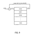
- FIG. 9 is a diagram useful for explaining the operation of the previously-considered arithmetic unit.
- the data ⁇ 2 read from the address "0000" of the DP-RAM 11 one clock earlier is added to newly inputted data, and this new result of computation i.e. addition is written as the data ⁇ 1 into the same address "0000".
- the inputted data groups are sequentially added, and the result of additions can be outputted as data of integral values.
- the previously-considered arithmetic unit described above uses the DP-RAM 11, which enables the reading operation and writing operation to be carried out in parallel with each other, so that the computation can be carried out at a high processing speed.
- the DP-RAM 11 occupies a larger area than a SP-RAM (Single Port RAM), which makes it difficult to reduce the size of the arithmetic unit.
- an arithmetic unit that receives a data group formed of a plurality of data, and performs a predetermined arithmetic processing operation between the data group and another data group inputted earlier.
- This arithmetic unit is characterized by comprising input portion for inputting data of the data group, first to n-th (n > 1) storage portion each having a capacity capable of storing at least part or all of the data group, readout portion for selecting one of the first to n-th storage portion and reading out therefrom a data group already stored therein, arithmetic portion for performing a predetermined arithmetic operation between the data group read out by the readout portion and the data group newly inputted by the input portion, and writing portion for writing a result of the predetermined arithmetic operation by the arithmetic portion in a predetermined one of the storage portion, which is not selected by the readout portion as the one from which the data group already stored therein is to be read out.
- a receiver unit that receives a data group formed of a plurality of data, and performs a predetermined arithmetic processing operation between the data group and another data group inputted earlier.
- This receiver unit is characterized by comprising input portion for inputting data of the data group, first to n-th (n > 1) storage portion each having a capacity capable of storing at least part or all of the data group, readout portion for selecting one of the first to n-th storage portion and reading out therefrom a data group already stored therein, arithmetic portion for performing a predetermined arithmetic operation between the data group read out by the readout portion and the data group newly inputted by the input portion, and writing portion for writing a result of the predetermined arithmetic operation by the arithmetic portion in a predetermined one of the storage portion, which is not selected by the readout portion as the one from which the data group already stored therein is to be read out.
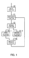
- FIG. 1 illustrates the principles of operation of an arithmetic unit embodying the present invention.
- an arithmetic unit embodying the present invention is comprised of an input portion 20, an arithmetic portion 21, a writing portion 22, a first storage portion 23-1, a second storage portion 23-2, and a readout portion 24.
- This figure corresponds to a case in which "n" in appended Claim 1 is equal to 2.
- the input portion 20 inputs a data group used for computation (arithmetic operation).
- the arithmetic portion 21 performs a predetermined arithmetic operation between a data group read out by the readout portion 24 and a data group newly inputted by the input portion 20.
- the writing portion 22 writes results of the arithmetic operation by the arithmetic portion 21 into a predetermined storage portion from which data are not to be read out by the readout portion 24.
- the first storage portion 23-1 and the second storage portion 23-2 each have a capacity capable of storing at least part or all of a data group.
- the readout portion 24 selects either the first storage portion 23-1 or the second storage portion 23-2, and reads from the selected data group already stored therein.
- the first storage portion 23-1 and the second storage portion 23-2 are initialized by using an initial value "0".
- the input portion 20 starts inputting of the first data group.
- the readout portion 24 reads data stored in an address "0000" of the first storage portion 23-1 (in the present case, the initial value "0") and supplies the read data to the arithmetic portion 21.
- the arithmetic portion 21 adds the data inputted by the input portion 20 and the data supplied by the readout portion 24 and supplies the result of the addition to the writing portion 22.
- the data supplied from the readout portion 24 is the initial value "0", and hence the data inputted by the input portion 20 is supplied to the writing portion 22 without any change.
- the writing portion 22 writes the data outputted from the arithmetic portion 21 in an address "0000" of the second storage portion 23-2 from which data are not to be read by the readout portion 21.
- FIG. 2 is a diagram useful for explaining the outline of the above operation. As shown in this figure, the data read out from the address "0000" of the first storage portion 23-1 (initial value "0" in the present case) is added to the first data of the inputted data group, and the resulting sum or data is stored in the address "0000" of the second storage portion 23-2.
- the readout portion 24 reads out data from an address "0001" of the first storage portion 23-1, and supplies the read data to the arithmetic portion 21.
- the arithmetic portion 21 adds the data supplied by the input portion 20 and the data supplied by the readout portion 24 and supplies the resulting data to the writing portion 22.
- the writing portion 22 stores the data supplied from the arithmetic portion 21 into an address "0001" of the second storage portion 23-2.
- FIG. 3 is a diagram useful for explaining the outline of the above operation. As shown in this figure, the data read from the address "0001" of the fist storage portion 23-1 (initial value "0" in the present case) is added to the inputted second data of the first data group, and the resulting data is stored in the address "0001" of the second storage portion 23-2.
- the writing portion 22 and the readout portion 24 exchange storage portion in which data are to be written and from which data are to be read. More specifically, now the writing portion 22 uses the first storage portion 23-1 as the storage portion into which data are written and the readout portion 24 uses the second storage portion 23-2 as the storage portion from which data are read.
- the arithmetic portion 21 adds the data supplied by the readout portion 24 and the data supplied by the input portion 20, and supplies the resulting data to the writing portion 22.
- the readout portion 24 supplies the data stored in the address "0000" of the second storage portion 23-2, and hence the arithmetic portion 21 adds the data stored in the address "0000" of the second storage portion 23-2 (first data of the first data group) and the first data of the second data group inputted by the input portion 20, and supplies the resulting data to the writing portion 22.
- the writing portion 22 writes the data supplied from the arithmetic portion 21 into the address "0000" of the first storage portion 23-1.
- FIG. 4 is a diagram useful for explaining the outline of the above operation. As shown in this figure, the data read from the address "0000" of the second storage portion 23-2 (first data of the first data group in the present example) is added to the first data of the second data group and the resulting data is stored in the address "0000" of the first storage portion 23-1.
- the input portion 20 inputs a second data of the second data group, and the readout portion 24 reads out the data stored in the address "0001" of the second storage portion 23-2 (second data of the first data group), and supplies the read data to the arithmetic portion 21.
- the arithmetic portion 21 adds the data inputted by the input portion 20 and the data supplied by the readout portion 24, and supplies the resulting data to the writing portion 22.
- the second data of the first data group is supplied by the readout portion 24, while the second data of the second data group is supplied by the input portion 20, and data of the result of the addition is supplied to the writing portion 22.
- the writing portion 22 stores the data supplied from the arithmetic portion 21 in the address "0001" of the first storage portion 23-1.
- FIG. 5 is a diagram useful for explaining the outline of the above operation. As shown in this figure, the data read from the address "0001" of the second storage portion 23-2 (second data of the first data group in the present example) is added to the inputted second data of the second data group, and the resulting data is stored in the address "0001" of the first storage portion 23-1.
- processing on a third data group is carried out.
- the data stored in the first storage portion 23-1 sums of respective corresponding data of the first data group and the second data group
- data of the third data group newly inputted by the input portion 20 are sequentially added, and the resulting sums are sequentially stored in the second storage portion 23-2.
- processing on the third data group is completed, then, processing on a fourth data group is executed.
- processing on a fourth data group is executed.
- the same operations are repeatedly carried out until processing on all the data groups is completed.
- the storage portion (first or second storage portion) into which the writing portion 23-1 finally writes data stores data of cumulative additions (integrations) of all the respective corresponding data of the first to m-th data groups.
- SP-RAMs for example, as the storage portion. Therefore, it is possible to reduce the size of the arithmetic unit, and realize a high speed arithmetic processing operation similarly to the case in which the DP-RAM is used.
- the arithmetic operation is carried out on all of the data groups inputted by the input portion 20, and the resulting sums are stored in the first storage portion 23-1 and the second storage portion 23-2, this is not limitative, but it is also possible to carry out the arithmetic operation on part of the data groups, and store the resulting sums in the first storage portion 23-1 and the second storage portion 23-2.
- FIG. 6 is a diagram showing the arrangement of an arithmetic unit according to an embodiment of the invention.
- the arithmetic unit is comprised of an ADD 50, a storage section 51, a selector 52, an initializing section 53, an address generator 54, an R/W control section 55, and a control section 56.
- the ADD 50 adds inputted data (DATA) and data supplied from the selector 52, and supplies the resulting sum or data to a SP-RAM 51b.
- the storage section 51 is comprised of an SP-RAM 51a and the SP-RAM 51b.
- the storage section 51 serves as an SP-RAM which is designated by a control signal from the R/W control section 55, and from which is read out data stored in an address thereof corresponding to a value of an address signal supplied from the address generator 54, and an SP-RAM from which data is not read, and into which is stored a result of arithmetic operation by the ADD 50, at an address corresponding to a value of an address signal supplied by the address generator 54.
- the selector 52 selects one of the SP-RAMs which is designated by the R/W control section 55 as one from which data are to be read out, and supplies the read or output data to the initializing section 53.
- the initializing section 53 initializes all the data outputted from the selector 52 to "0" when the first data group is inputted, and supplies the resulting data to the ADD 50.
- the address generator 54 generates the address signals according to the control of the control section 56, and supplies the address signals to the SP-RAM 51a and the SP-RAM 51b, respectively.
- the R/W control section 55 is under the control of the control section 56 and designates one of the SP-RAM 51a and the SP-RAM 51b as one from which data are to be read out and the other of them as one into which data are to be written.
- the control section 56 controls the address generator 54, the R/W control section 55, and the selector 52.
- FIG. 7 is a timing chart for explaining the operation of the arithmetic unit embodying the present embodiment. Hereafter, the operation of the FIG. 6 arithmetic unit will be explained by referring to FIG. 7 as required.
- control section 56 instructs the initializing section 53 to carry out initialization. Further, the control section 56 instructs the address generator 54 to generate the address signals, and at the same time instructs the R/W control section 55 to generate the R/W signal.
- the address generator 54 Responsive to the instruction from the control section 56, the address generator 54 performs operations of counting up from “0" to the maximum address "10239", and when the maximum address is reached, the counting operation is carried out in a circulating fashion to start counting up again from "0". Further, the most significant bit (MSB) of the address signal outputted from the address generator 54 contains a signal for designating one of the SP-RAM 51a and the SP-RAM 51b as one from which data are to be read out (or one into which data are to be written).
- MSB most significant bit
- the SP-RAM 51a and the SP-RAM 51b are supplied with respective address signals ADD 1 and ADD 2 from which the most significant bit (MSB) is omitted, and hence these address signals provide signals circulating from the value "0" to the value "10239" (see FIG. 7 (E), (F)).
- the R/W control section 55 sets an R/W1 signal to "L”, an R/W2 signal to "H”, and an R/W3 signal to "L”. Further, when the MSB of the data from the address generator 54 is "1", the R/W control section 55 sets the R/W1 signal to "H”, the R/W2 signal to "L”, and the R/W3 signal to "H” (see FIG. 7 (B) to (D)).
- the ADD 50 adds data ⁇ 2 from the initialing section 53 and inputted data ("100": see FIG. 7 (G)), and outputs the resulting data.
- the initializing section 53 is instructed by the control section 56 to carry out the initialization, "0" is supplied as the data ⁇ 2 to the ADD 50 irrespective of the value of the data outputted from the selector 52 (see FIG. 7 (I)).
- the address generator 54 has outputted the respective address signals ADD 1, ADD 2 having the value of "0" to the SP-RAM 51a and the SP-RAM 51b. Further, the MSB of each address signal is "0", so that the R/W control section 55 outputs "L” as the R/W1 signal, "H” as the R/W2 signal, and "L” as the R/W3 signal (see FIG. 7 (B) to (D)).
- the SP-RAM 51a is set to a readable state
- the SP-RAM 51b is set to a writable state
- the selector 52 is placed in a state selecting the output from the SP-RAM 51a.
- the data "100" outputted from the ADD 50 is stored in the address "0" of the SP-RAM 51b.
- the address generator 54 increments the address value by "1", thereby generating the address signals ADD 1, ADD 2 having the value "1", and supplies the signals to the SP-RAM 51a and the SP-RAM 51b, respectively.
- the MSB of the address signals is not changed, and hence the SP-RAM 51a continues to be the one from which data are to be read, and the SP-RAM 51b continues to be the one into which data are to be written. Further, since the initializing section 53 outputs the value "0", the ADD 50 adds the value "0" and the inputted data "150” (see FIG. 7 (G)) and writes the resulting data "150” into the address "1" of the SP-RAM 51b.
- the address generator 54 sets the MSB to "1", and sets all the other bits to "0".
- the R/W control section 55 sets the R/W1 signal to "H", the R/W2 signal to "L”, and the R/W3 signal to "H”, whereby the SP-RAM 51a is set to the writable state and the SP-RAM 51b is set to the readable state, respectively, and the selector 52 selects and outputs an output from the SP-RAM 51b.
- control section 56 instructs the initializing section 53 to terminate the initialization, so that the initializing section 53 supplies the data outputted from the selector 52 to the ADD 50 without causing any change of the data.
- the SP-RAM 51b reads out and outputs data (first data "100" of the first data group) stored in the address "0" thereof.
- the selector 52 selects the data supplied from the SP-RAM 51b, and supplies the same to the initializing section 53.
- the initializing section 53 supplies the data "100” outputted from the selector 52 to the ADD 50 without causing any change of the data.
- the ADD 50 adds the data "100” outputted from the initializing section 53 and a newly inputted data "477", and stores the resulting data "577” in the address "0" of the SP-RAM 51a.
- the address generator 54 increments the address value by "1", and outputs the address signals ADD 1, ADD 2 having resulting value "1".
- the address generator 54 increments the address value by "1", and outputs the address signals ADD 1, ADD 2 having resulting value "1".
- the ADD 50 adds a newly inputted data "144" and the data "150” supplied from the initializing section 53, and supplies the resulting data "294" to the SP-RAM 51a.
- the SP-RAM 51a stores the supplied data "294" in the address "1" thereof.
- the SP-RAM 51a stores values obtained by adding data of the first data group and data of the second data group, respectively.
- the MSB is set to "0", and the bits other than the MSB are set to "0", whereby the arithmetic operation is carried out by setting the SP-RAM 51a to the one from which data are to be read, and the SP-RAM 51b to the one into which data are to be written.
- the above processing operations are repeatedly carried out a predetermined number of times preset by the control section 56, and when additions of all data of all data groups are completed, the data are read from one of the SP-RAMs in which the ultimate results of additions are stored whereby the results of the arithmetic operation can be obtained.
- a plurality of SP-RAMs are provided for using each of them alternately as storage portion from which data are to be read and storage portion into which data are to be written to thereby cumulatively adding inputted data of data groups.
- the number of times of the arithmetic operation performed in units of blocks may be counted, and when the counted number reaches a predetermined value, the arithmetic operation may be stopped. According to such an embodiment of the invention, it is possible to calculate an integral or cumulative value of data according to the set value.
- the number of times of the arithmetic operation performed in units of blocks may be changed in dependence on circumstance of operation or the like. According to such an embodiment of the invention, the optimum operation dependent on the objective or the environment of use of the arithmetic unit can be carried out.
- the two SP-RAMs are used, this is not limitative, but the number of SP-RAMs may be three or more. In such cases, by using a plurality of most significant bits, a desired one of the SP-RAMs can be selected.
- the MSB is used as a bit for use in selection, this is not limitative, but it goes without saying that the LSB or other bit may be used for the same purpose.
- the initializing section 53 is interposed between the selector 52 and the ADD 50, and the initialization is carried out when the arithmetic operation is executed a first time, this is not limitative, but it goes without saying that various variations of the embodiment can be contemplated. What is required is that data outputted by the ADD 50 in the first cycle of the arithmetic operation carried out on the first data group are equal to the inputted data.
- an arithmetic unit receives a data group formed of a plurality of data, and performs a predetermined arithmetic processing operation between the data group and another data group inputted earlier.
- the arithmetic unit comprises an input portion for inputting data of the data group, first to n-th (n > 1) storage portions each having a capacity capable of storing at least part or all of the data group, a readout portion for selecting one of the first to n-th storage portions and reading out therefrom a data group already stored therein, an arithmetic portion for performing a predetermined arithmetic operation between the data group read out by the readout portion and the data group newly inputted by the input portion, and a writing portion for writing a result of the predetermined arithmetic operation of the arithmetic portion in a predetermined one of the storage portion, which is not selected by the readout portion as the one from which the data group already stored therein is to be read out. Therefore, it is possible to carry out the arithmetic operation at a high speed and at the same time reduce the size of the arithmetic unit.
- a receiver unit receives a data group formed of a plurality of data, and performs a predetermined arithmetic processing operation between the data group and another data group inputted earlier.
- the receiver unit comprises an input portion for inputting data of the data group, first to n-th (n > 1) storage portions each having a capacity capable of storing at least part or all of the data group, a readout portion for selecting one of the first to n-th storage portions and reading out therefrom a data group already stored therein, an arithmetic portion for performing a predetermined arithmetic operation between the data group read out by the readout portion and the data group newly inputted by the input portion, and a writing portion for writing a result of the predetermined arithmetic operation of the arithmetic portion in a predetermined one of the storage portion, which is not selected by the readout portion as the one from which the data group already stored therein is to be read out. Therefore, it is possible to receive the data
Landscapes
- Engineering & Computer Science (AREA)
- Theoretical Computer Science (AREA)
- Software Systems (AREA)
- Physics & Mathematics (AREA)
- General Physics & Mathematics (AREA)
- General Engineering & Computer Science (AREA)
- Computational Mathematics (AREA)
- Pure & Applied Mathematics (AREA)
- Mathematical Optimization (AREA)
- Mathematical Analysis (AREA)
- Complex Calculations (AREA)
- Executing Machine-Instructions (AREA)
- Communication Control (AREA)
- Compression, Expansion, Code Conversion, And Decoders (AREA)
- Image Processing (AREA)
Abstract
Description
Claims (12)
- An arithmetic unit that receives a data group formed of a plurality of data, and performs a predetermined arithmetic processing operation between the data group and another data group inputted earlier,
the arithmetic unit comprising:an input portion for inputting data of the data group;first to n-th (n > 1) storage portions each having a capacity capable of storing at least part or all of the data group;a readout portion for selecting one of the first to n-th storage portions and reading out therefrom a data group already stored therein;an arithmetic portion for performing a predetermined arithmetic operation between the data group read out by the readout portion and the data group newly inputted by the input portion; andwriting portion for writing a result of the predetermined arithmetic operation by the arithmetic portion in one of the first to n-th storage portions, wherein the storage portion in which the result is to be written is not selected by the readout portion as the one from which the data group already stored therein is to be read out. - A receiver unit that receives a data group formed of a plurality of data, and performs a predetermined arithmetic processing operation between the data group and another data group inputted earlier,
the receiver unit comprising:an input portion for inputting data of the data group;first to n-th (n > 1) storage portions each having a capacity capable of storing at least part or all of the data group;a readout portion for selecting one of the first to n-th storage portions and reading out therefrom a data group already stored therein;an arithmetic portion for performing a predetermined arithmetic operation between the data group read out by the readout portion and the data group newly inputted by the input portion; anda writing portion for writing a result of the predetermined arithmetic operation by the arithmetic portion in one of the first to n-th storage portions, wherein the storage portion in which the result is to be written is not selected by the readout portion as the one from which the data group already stored therein is to be read out. - The arithmetic unit or the receiver unit, as the case may be, according to claim 1 or 2, further comprising output portion for outputting data of the result of the predetermined arithmetic operation stored in one of the first to n-th storage portion.
- The arithmetic unit or the receiver unit, as the case may be, according to claim 1, 2 or 3, wherein the first to n-th storage portion are formed by a memory array, and wherein the memory array is used in a bank switching manner so as to be used as the first to n-th storage portion.
- The arithmetic unit or the receiver unit, as the case may be, according to claim 4, wherein the memory array is formed by single port memories.
- The arithmetic unit or the receiver unit, as the case may be, according to any preceding claim, further comprising address-generating portion for generating addresses which are accessed by the readout portion and the writing portion, and
wherein by using a predetermined bit of each address generated by the address-generating portion, ones of the first to n-th storage portion which are to be accessed by the readout portion and the writing portion are specified. - The arithmetic unit or the receiver unit, as the case may be, according to any preceding claim, wherein the readout portion reads out data prior to writing by the writing portion.
- The arithmetic unit or the receiver unit, as the case may be, according to any preceding claim, wherein the arithmetic portion executes addition to thereby perform integrating operation in units of data groups.
- The arithmetic unit or the receiver unit, as the case may be, according to any preceding claim, comprising:operation start-instructing portion for instructing the predetermined arithmetic processing operation to be started, andinitializing portion for setting all data of a first data group supplied from the readout portion to an initial value of "0" when the operation start-instructing portion instructs the predetermined arithmetic processing operation to be started.
- The arithmetic unit or the receiver unit, as the case may be, according to any preceding claim, further comprising:counting portion for counting a number of times of the arithmetic processing operations performed in units of blocks, andstoppage portion for stopping the predetermined arithmetic processing operation when a value counted by the counting portion reaches a predetermined set value.
- The arithmetic unit or the receiver unit, as the case may be, according to any preceding claim, further comprising set value-changing portion for changing the predetermined set value.
- A data processing method in which a data group formed of a plurality of data is received, and a predetermined arithmetic processing operation is performed between the data group and another data group inputted earlier,
said method comprising the steps of:(a) inputting data of the data group;(b) selecting one of first to n-th (n>1) storage portions, each having a capacity capable of storing at least part or all of the data group, and reading out therefrom a data group already stored therein;(c) performing a predetermined arithmetic operation between the data group read out in step (b) and the data group newly inputted in step (a); and(d) writing a result of the predetermined arithmetic operation performed in step (c) in one of the first to n-th storage portions, wherein the storage portion in which the result is to be written is not selected in step (b) as the one from which the data group already stored therein is to be read out.
Applications Claiming Priority (2)
| Application Number | Priority Date | Filing Date | Title |
|---|---|---|---|
| JP2001204162A JP4278317B2 (en) | 2001-07-05 | 2001-07-05 | Arithmetic device and receiving device |
| JP2001204162 | 2001-07-05 |
Publications (3)
| Publication Number | Publication Date |
|---|---|
| EP1274006A2 true EP1274006A2 (en) | 2003-01-08 |
| EP1274006A3 EP1274006A3 (en) | 2005-11-16 |
| EP1274006B1 EP1274006B1 (en) | 2010-01-20 |
Family
ID=19040669
Family Applications (1)
| Application Number | Title | Priority Date | Filing Date |
|---|---|---|---|
| EP20020251691 Expired - Lifetime EP1274006B1 (en) | 2001-07-05 | 2002-03-11 | Arithmetic unit and receiver unit |
Country Status (4)
| Country | Link |
|---|---|
| US (1) | US6947961B2 (en) |
| EP (1) | EP1274006B1 (en) |
| JP (1) | JP4278317B2 (en) |
| DE (1) | DE60235139D1 (en) |
Families Citing this family (3)
| Publication number | Priority date | Publication date | Assignee | Title |
|---|---|---|---|---|
| US7394561B2 (en) * | 2002-08-28 | 2008-07-01 | Kabushiki Kaisha Toshiba | Image forming apparatus |
| JP4765260B2 (en) * | 2004-03-31 | 2011-09-07 | 日本電気株式会社 | Data processing device, processing method thereof, program, and mobile phone device |
| JP4724031B2 (en) * | 2006-03-28 | 2011-07-13 | 三菱プレシジョン株式会社 | Computer and computer system using synchronized stack memory |
Family Cites Families (11)
| Publication number | Priority date | Publication date | Assignee | Title |
|---|---|---|---|---|
| DE3066955D1 (en) * | 1980-06-24 | 1984-04-19 | Ibm | Signal processor computing arrangement and method of operating said arrangement |
| US4689762A (en) * | 1984-09-10 | 1987-08-25 | Sanders Associates, Inc. | Dynamically configurable fast Fourier transform butterfly circuit |
| JPH0520139A (en) | 1991-07-15 | 1993-01-29 | Hokkaido Nippon Denki Software Kk | Source unit deleting system |
| JPH0566751A (en) | 1991-09-10 | 1993-03-19 | Matsushita Electric Ind Co Ltd | Gradation correcting circuit |
| US5371877A (en) * | 1991-12-31 | 1994-12-06 | Apple Computer, Inc. | Apparatus for alternatively accessing single port random access memories to implement dual port first-in first-out memory |
| GB2291515B (en) * | 1994-07-14 | 1998-11-18 | Advanced Risc Mach Ltd | Data processing using multiply-accumulate instructions |
| US6061783A (en) * | 1996-11-13 | 2000-05-09 | Nortel Networks Corporation | Method and apparatus for manipulation of bit fields directly in a memory source |
| JP2760352B1 (en) * | 1996-11-29 | 1998-05-28 | 日本電気株式会社 | Cell search circuit for CDMA |
| DE69837299T2 (en) * | 1997-01-22 | 2007-06-28 | Matsushita Electric Industrial Co., Ltd., Kadoma | System and method for fast Fourier transformation |
| US6191998B1 (en) * | 1997-10-16 | 2001-02-20 | Altera Corporation | Programmable logic device memory array circuit having combinable single-port memory arrays |
| US6363060B1 (en) * | 1999-06-30 | 2002-03-26 | Qualcomm Incorporated | Method and apparatus for fast WCDMA acquisition |
-
2001
- 2001-07-05 JP JP2001204162A patent/JP4278317B2/en not_active Expired - Fee Related
-
2002
- 2002-02-21 US US10/078,368 patent/US6947961B2/en not_active Expired - Lifetime
- 2002-03-11 EP EP20020251691 patent/EP1274006B1/en not_active Expired - Lifetime
- 2002-03-11 DE DE60235139T patent/DE60235139D1/en not_active Expired - Lifetime
Also Published As
| Publication number | Publication date |
|---|---|
| US20030009499A1 (en) | 2003-01-09 |
| JP2003015862A (en) | 2003-01-17 |
| JP4278317B2 (en) | 2009-06-10 |
| EP1274006B1 (en) | 2010-01-20 |
| EP1274006A3 (en) | 2005-11-16 |
| DE60235139D1 (en) | 2010-03-11 |
| US6947961B2 (en) | 2005-09-20 |
Similar Documents
| Publication | Publication Date | Title |
|---|---|---|
| EP1472604B1 (en) | Reconfigurable parallel look up table system | |
| US20080307196A1 (en) | Integrated Processor Array, Instruction Sequencer And I/O Controller | |
| CN112712457B (en) | Data processing method and artificial intelligence processor | |
| CN113885831A (en) | Storage and calculation integrated circuit based on mixed data input, chip and calculation device | |
| US5551019A (en) | Methods and systems for sorting multiplying indexed data | |
| US20080126758A1 (en) | Digital signal processing apparatus and method for multiply-and-accumulate operation | |
| US6665768B1 (en) | Table look-up operation for SIMD processors with interleaved memory systems | |
| JP2022074442A (en) | Arithmetic device and arithmetic method | |
| EP1462931B1 (en) | Method for referring to address of vector data and vector processor | |
| US6947961B2 (en) | Arithmetic unit and receiver unit | |
| JP3587675B2 (en) | Pseudo noise generator | |
| JP3032340B2 (en) | Address generator for processor data memory | |
| JPH11110339A (en) | DMA controller | |
| US6577676B1 (en) | Digital matched filter | |
| JP2856064B2 (en) | Digital filter | |
| JP2851804B2 (en) | 2D orthogonal transform device | |
| JP4984438B2 (en) | Memory test apparatus and memory test method | |
| JP5072558B2 (en) | Data processing device | |
| US6502179B2 (en) | Method and apparatus for compactly storing instruction codes | |
| JP3042266B2 (en) | Memory access method | |
| JP2003150576A (en) | FFT operation device and FFT operation method | |
| JP3271155B2 (en) | Data controller | |
| JP3126430B2 (en) | Pattern generation circuit | |
| JP2761559B2 (en) | Data generator for semiconductor memory test | |
| JP3078138B2 (en) | Variable length code generator |
Legal Events
| Date | Code | Title | Description |
|---|---|---|---|
| PUAI | Public reference made under article 153(3) epc to a published international application that has entered the european phase |
Free format text: ORIGINAL CODE: 0009012 |
|
| AK | Designated contracting states |
Kind code of ref document: A2 Designated state(s): AT BE CH CY DE DK ES FI FR GB GR IE IT LI LU MC NL PT SE TR |
|
| AX | Request for extension of the european patent |
Free format text: AL;LT;LV;MK;RO;SI |
|
| PUAL | Search report despatched |
Free format text: ORIGINAL CODE: 0009013 |
|
| AK | Designated contracting states |
Kind code of ref document: A3 Designated state(s): AT BE CH CY DE DK ES FI FR GB GR IE IT LI LU MC NL PT SE TR |
|
| AX | Request for extension of the european patent |
Extension state: AL LT LV MK RO SI |
|
| RIC1 | Information provided on ipc code assigned before grant |
Ipc: 7G 06F 9/30 A Ipc: 7H 04B 1/707 B Ipc: 7G 06F 7/50 B |
|
| 17P | Request for examination filed |
Effective date: 20060118 |
|
| AKX | Designation fees paid |
Designated state(s): DE FR GB |
|
| 17Q | First examination report despatched |
Effective date: 20070202 |
|
| RAP1 | Party data changed (applicant data changed or rights of an application transferred) |
Owner name: FUJITSU MICROELECTRONICS LIMITED |
|
| GRAP | Despatch of communication of intention to grant a patent |
Free format text: ORIGINAL CODE: EPIDOSNIGR1 |
|
| GRAS | Grant fee paid |
Free format text: ORIGINAL CODE: EPIDOSNIGR3 |
|
| GRAA | (expected) grant |
Free format text: ORIGINAL CODE: 0009210 |
|
| AK | Designated contracting states |
Kind code of ref document: B1 Designated state(s): DE FR GB |
|
| REG | Reference to a national code |
Ref country code: GB Ref legal event code: FG4D |
|
| REF | Corresponds to: |
Ref document number: 60235139 Country of ref document: DE Date of ref document: 20100311 Kind code of ref document: P |
|
| PLBE | No opposition filed within time limit |
Free format text: ORIGINAL CODE: 0009261 |
|
| STAA | Information on the status of an ep patent application or granted ep patent |
Free format text: STATUS: NO OPPOSITION FILED WITHIN TIME LIMIT |
|
| REG | Reference to a national code |
Ref country code: FR Ref legal event code: ST Effective date: 20101130 |
|
| 26N | No opposition filed |
Effective date: 20101021 |
|
| GBPC | Gb: european patent ceased through non-payment of renewal fee |
Effective date: 20100420 |
|
| PG25 | Lapsed in a contracting state [announced via postgrant information from national office to epo] |
Ref country code: FR Free format text: LAPSE BECAUSE OF NON-PAYMENT OF DUE FEES Effective date: 20100331 |
|
| PG25 | Lapsed in a contracting state [announced via postgrant information from national office to epo] |
Ref country code: GB Free format text: LAPSE BECAUSE OF NON-PAYMENT OF DUE FEES Effective date: 20100420 |
|
| REG | Reference to a national code |
Ref country code: DE Ref legal event code: R082 Ref document number: 60235139 Country of ref document: DE Representative=s name: REICHERT & LINDNER PARTNERSCHAFT PATENTANWAELT, DE |
|
| REG | Reference to a national code |
Ref country code: DE Ref legal event code: R081 Ref document number: 60235139 Country of ref document: DE Owner name: SOCIONEXT INC., YOKOHAMA-SHI, JP Free format text: FORMER OWNER: FUJITSU SEMICONDUCTOR LTD., YOKOHAMA, KANAGAWA, JP Effective date: 20150512 Ref country code: DE Ref legal event code: R082 Ref document number: 60235139 Country of ref document: DE Representative=s name: REICHERT & LINDNER PARTNERSCHAFT PATENTANWAELT, DE Effective date: 20150512 |
|
| PGFP | Annual fee paid to national office [announced via postgrant information from national office to epo] |
Ref country code: DE Payment date: 20180227 Year of fee payment: 17 |
|
| REG | Reference to a national code |
Ref country code: DE Ref legal event code: R119 Ref document number: 60235139 Country of ref document: DE |
|
| PG25 | Lapsed in a contracting state [announced via postgrant information from national office to epo] |
Ref country code: DE Free format text: LAPSE BECAUSE OF NON-PAYMENT OF DUE FEES Effective date: 20191001 |