EP1273039B1 - Process for semiconductor wafer-level chip scale packages - Google Patents
Process for semiconductor wafer-level chip scale packages Download PDFInfo
- Publication number
- EP1273039B1 EP1273039B1 EP01924799A EP01924799A EP1273039B1 EP 1273039 B1 EP1273039 B1 EP 1273039B1 EP 01924799 A EP01924799 A EP 01924799A EP 01924799 A EP01924799 A EP 01924799A EP 1273039 B1 EP1273039 B1 EP 1273039B1
- Authority
- EP
- European Patent Office
- Prior art keywords
- layer
- chip
- wafer
- vias
- substrate
- Prior art date
- Legal status (The legal status is an assumption and is not a legal conclusion. Google has not performed a legal analysis and makes no representation as to the accuracy of the status listed.)
- Expired - Lifetime
Links
Images





















Classifications
-
- H—ELECTRICITY
- H10—SEMICONDUCTOR DEVICES; ELECTRIC SOLID-STATE DEVICES NOT OTHERWISE PROVIDED FOR
- H10W—GENERIC PACKAGES, INTERCONNECTIONS, CONNECTORS OR OTHER CONSTRUCTIONAL DETAILS OF DEVICES COVERED BY CLASS H10
- H10W20/00—Interconnections in chips, wafers or substrates
- H10W20/40—Interconnections external to wafers or substrates, e.g. back-end-of-line [BEOL] metallisations or vias connecting to gate electrodes
- H10W20/482—Interconnections external to wafers or substrates, e.g. back-end-of-line [BEOL] metallisations or vias connecting to gate electrodes for individual devices provided for in groups H10D8/00 - H10D48/00, e.g. for power transistors
- H10W20/484—Interconnections having extended contours, e.g. pads having mesh shape or interconnections comprising connected parallel stripes
-
- H—ELECTRICITY
- H10—SEMICONDUCTOR DEVICES; ELECTRIC SOLID-STATE DEVICES NOT OTHERWISE PROVIDED FOR
- H10P—GENERIC PROCESSES OR APPARATUS FOR THE MANUFACTURE OR TREATMENT OF DEVICES COVERED BY CLASS H10
- H10P72/00—Handling or holding of wafers, substrates or devices during manufacture or treatment thereof
- H10P72/70—Handling or holding of wafers, substrates or devices during manufacture or treatment thereof for supporting or gripping
- H10P72/74—Handling or holding of wafers, substrates or devices during manufacture or treatment thereof for supporting or gripping using temporarily an auxiliary support
-
- H—ELECTRICITY
- H10—SEMICONDUCTOR DEVICES; ELECTRIC SOLID-STATE DEVICES NOT OTHERWISE PROVIDED FOR
- H10W—GENERIC PACKAGES, INTERCONNECTIONS, CONNECTORS OR OTHER CONSTRUCTIONAL DETAILS OF DEVICES COVERED BY CLASS H10
- H10W20/00—Interconnections in chips, wafers or substrates
- H10W20/01—Manufacture or treatment
- H10W20/021—Manufacture or treatment of interconnections within wafers or substrates
- H10W20/023—Manufacture or treatment of interconnections within wafers or substrates the interconnections being through-semiconductor vias
-
- H—ELECTRICITY
- H10—SEMICONDUCTOR DEVICES; ELECTRIC SOLID-STATE DEVICES NOT OTHERWISE PROVIDED FOR
- H10W—GENERIC PACKAGES, INTERCONNECTIONS, CONNECTORS OR OTHER CONSTRUCTIONAL DETAILS OF DEVICES COVERED BY CLASS H10
- H10W20/00—Interconnections in chips, wafers or substrates
- H10W20/01—Manufacture or treatment
- H10W20/021—Manufacture or treatment of interconnections within wafers or substrates
- H10W20/023—Manufacture or treatment of interconnections within wafers or substrates the interconnections being through-semiconductor vias
- H10W20/0245—Manufacture or treatment of interconnections within wafers or substrates the interconnections being through-semiconductor vias comprising use of blind vias during the manufacture
-
- H—ELECTRICITY
- H10—SEMICONDUCTOR DEVICES; ELECTRIC SOLID-STATE DEVICES NOT OTHERWISE PROVIDED FOR
- H10W—GENERIC PACKAGES, INTERCONNECTIONS, CONNECTORS OR OTHER CONSTRUCTIONAL DETAILS OF DEVICES COVERED BY CLASS H10
- H10W20/00—Interconnections in chips, wafers or substrates
- H10W20/20—Interconnections within wafers or substrates, e.g. through-silicon vias [TSV]
-
- H—ELECTRICITY
- H10—SEMICONDUCTOR DEVICES; ELECTRIC SOLID-STATE DEVICES NOT OTHERWISE PROVIDED FOR
- H10W—GENERIC PACKAGES, INTERCONNECTIONS, CONNECTORS OR OTHER CONSTRUCTIONAL DETAILS OF DEVICES COVERED BY CLASS H10
- H10W72/00—Interconnections or connectors in packages
- H10W72/01—Manufacture or treatment
- H10W72/019—Manufacture or treatment of bond pads
-
- H—ELECTRICITY
- H10—SEMICONDUCTOR DEVICES; ELECTRIC SOLID-STATE DEVICES NOT OTHERWISE PROVIDED FOR
- H10W—GENERIC PACKAGES, INTERCONNECTIONS, CONNECTORS OR OTHER CONSTRUCTIONAL DETAILS OF DEVICES COVERED BY CLASS H10
- H10W74/00—Encapsulations, e.g. protective coatings
- H10W74/10—Encapsulations, e.g. protective coatings characterised by their shape or disposition
- H10W74/111—Encapsulations, e.g. protective coatings characterised by their shape or disposition the semiconductor body being completely enclosed
- H10W74/129—Encapsulations, e.g. protective coatings characterised by their shape or disposition the semiconductor body being completely enclosed forming a chip-scale package [CSP]
-
- H—ELECTRICITY
- H10—SEMICONDUCTOR DEVICES; ELECTRIC SOLID-STATE DEVICES NOT OTHERWISE PROVIDED FOR
- H10P—GENERIC PROCESSES OR APPARATUS FOR THE MANUFACTURE OR TREATMENT OF DEVICES COVERED BY CLASS H10
- H10P72/00—Handling or holding of wafers, substrates or devices during manufacture or treatment thereof
- H10P72/70—Handling or holding of wafers, substrates or devices during manufacture or treatment thereof for supporting or gripping
- H10P72/74—Handling or holding of wafers, substrates or devices during manufacture or treatment thereof for supporting or gripping using temporarily an auxiliary support
- H10P72/7426—Handling or holding of wafers, substrates or devices during manufacture or treatment thereof for supporting or gripping using temporarily an auxiliary support used as a support during build up manufacturing of active devices
-
- H—ELECTRICITY
- H10—SEMICONDUCTOR DEVICES; ELECTRIC SOLID-STATE DEVICES NOT OTHERWISE PROVIDED FOR
- H10W—GENERIC PACKAGES, INTERCONNECTIONS, CONNECTORS OR OTHER CONSTRUCTIONAL DETAILS OF DEVICES COVERED BY CLASS H10
- H10W46/00—Marks applied to devices, e.g. for alignment or identification
- H10W46/601—Marks applied to devices, e.g. for alignment or identification for use after dicing
- H10W46/603—Formed on wafers or substrates before dicing and remaining on chips after dicing
-
- H—ELECTRICITY
- H10—SEMICONDUCTOR DEVICES; ELECTRIC SOLID-STATE DEVICES NOT OTHERWISE PROVIDED FOR
- H10W—GENERIC PACKAGES, INTERCONNECTIONS, CONNECTORS OR OTHER CONSTRUCTIONAL DETAILS OF DEVICES COVERED BY CLASS H10
- H10W72/00—Interconnections or connectors in packages
- H10W72/01—Manufacture or treatment
- H10W72/012—Manufacture or treatment of bump connectors, dummy bumps or thermal bumps
- H10W72/01204—Manufacture or treatment of bump connectors, dummy bumps or thermal bumps using temporary auxiliary members, e.g. using sacrificial coatings or handle substrates
-
- H—ELECTRICITY
- H10—SEMICONDUCTOR DEVICES; ELECTRIC SOLID-STATE DEVICES NOT OTHERWISE PROVIDED FOR
- H10W—GENERIC PACKAGES, INTERCONNECTIONS, CONNECTORS OR OTHER CONSTRUCTIONAL DETAILS OF DEVICES COVERED BY CLASS H10
- H10W72/00—Interconnections or connectors in packages
- H10W72/071—Connecting or disconnecting
- H10W72/072—Connecting or disconnecting of bump connectors
- H10W72/07251—Connecting or disconnecting of bump connectors characterised by changes in properties of the bump connectors during connecting
-
- H—ELECTRICITY
- H10—SEMICONDUCTOR DEVICES; ELECTRIC SOLID-STATE DEVICES NOT OTHERWISE PROVIDED FOR
- H10W—GENERIC PACKAGES, INTERCONNECTIONS, CONNECTORS OR OTHER CONSTRUCTIONAL DETAILS OF DEVICES COVERED BY CLASS H10
- H10W72/00—Interconnections or connectors in packages
- H10W72/20—Bump connectors, e.g. solder bumps or copper pillars; Dummy bumps; Thermal bumps
-
- H—ELECTRICITY
- H10—SEMICONDUCTOR DEVICES; ELECTRIC SOLID-STATE DEVICES NOT OTHERWISE PROVIDED FOR
- H10W—GENERIC PACKAGES, INTERCONNECTIONS, CONNECTORS OR OTHER CONSTRUCTIONAL DETAILS OF DEVICES COVERED BY CLASS H10
- H10W72/00—Interconnections or connectors in packages
- H10W72/20—Bump connectors, e.g. solder bumps or copper pillars; Dummy bumps; Thermal bumps
- H10W72/241—Dispositions, e.g. layouts
- H10W72/242—Dispositions, e.g. layouts relative to the surface, e.g. recessed, protruding
-
- H—ELECTRICITY
- H10—SEMICONDUCTOR DEVICES; ELECTRIC SOLID-STATE DEVICES NOT OTHERWISE PROVIDED FOR
- H10W—GENERIC PACKAGES, INTERCONNECTIONS, CONNECTORS OR OTHER CONSTRUCTIONAL DETAILS OF DEVICES COVERED BY CLASS H10
- H10W72/00—Interconnections or connectors in packages
- H10W72/20—Bump connectors, e.g. solder bumps or copper pillars; Dummy bumps; Thermal bumps
- H10W72/241—Dispositions, e.g. layouts
- H10W72/244—Dispositions, e.g. layouts relative to underlying supporting features, e.g. bond pads, RDLs or vias
-
- H—ELECTRICITY
- H10—SEMICONDUCTOR DEVICES; ELECTRIC SOLID-STATE DEVICES NOT OTHERWISE PROVIDED FOR
- H10W—GENERIC PACKAGES, INTERCONNECTIONS, CONNECTORS OR OTHER CONSTRUCTIONAL DETAILS OF DEVICES COVERED BY CLASS H10
- H10W72/00—Interconnections or connectors in packages
- H10W72/20—Bump connectors, e.g. solder bumps or copper pillars; Dummy bumps; Thermal bumps
- H10W72/29—Bond pads specially adapted therefor
-
- H—ELECTRICITY
- H10—SEMICONDUCTOR DEVICES; ELECTRIC SOLID-STATE DEVICES NOT OTHERWISE PROVIDED FOR
- H10W—GENERIC PACKAGES, INTERCONNECTIONS, CONNECTORS OR OTHER CONSTRUCTIONAL DETAILS OF DEVICES COVERED BY CLASS H10
- H10W72/00—Interconnections or connectors in packages
- H10W72/90—Bond pads, in general
- H10W72/921—Structures or relative sizes of bond pads
- H10W72/926—Multiple bond pads having different sizes
-
- H—ELECTRICITY
- H10—SEMICONDUCTOR DEVICES; ELECTRIC SOLID-STATE DEVICES NOT OTHERWISE PROVIDED FOR
- H10W—GENERIC PACKAGES, INTERCONNECTIONS, CONNECTORS OR OTHER CONSTRUCTIONAL DETAILS OF DEVICES COVERED BY CLASS H10
- H10W72/00—Interconnections or connectors in packages
- H10W72/90—Bond pads, in general
- H10W72/931—Shapes of bond pads
- H10W72/932—Plan-view shape, i.e. in top view
-
- H—ELECTRICITY
- H10—SEMICONDUCTOR DEVICES; ELECTRIC SOLID-STATE DEVICES NOT OTHERWISE PROVIDED FOR
- H10W—GENERIC PACKAGES, INTERCONNECTIONS, CONNECTORS OR OTHER CONSTRUCTIONAL DETAILS OF DEVICES COVERED BY CLASS H10
- H10W72/00—Interconnections or connectors in packages
- H10W72/90—Bond pads, in general
- H10W72/941—Dispositions of bond pads
- H10W72/942—Dispositions of bond pads relative to underlying supporting features, e.g. bond pads, RDLs or vias
-
- H—ELECTRICITY
- H10—SEMICONDUCTOR DEVICES; ELECTRIC SOLID-STATE DEVICES NOT OTHERWISE PROVIDED FOR
- H10W—GENERIC PACKAGES, INTERCONNECTIONS, CONNECTORS OR OTHER CONSTRUCTIONAL DETAILS OF DEVICES COVERED BY CLASS H10
- H10W72/00—Interconnections or connectors in packages
- H10W72/90—Bond pads, in general
- H10W72/941—Dispositions of bond pads
- H10W72/944—Dispositions of multiple bond pads
Definitions
- This invention relates to wafer-level packaging techniques for semiconductor chips and in particular to packaging techniques for semiconductor chips that contain devices or components, such as vertical power MOSFETs that have terminals on both sides of the chip.
- the resulting semiconductor chips which could be integrated circuit (IC) or MOSFET chips for example, must be separated and packaged in such a way that they can be connected to external circuitry.
- IC integrated circuit
- MOSFET chips MOSFET chips for example.
- packaging techniques Most involve mounting the chip on a leadframe, connecting the chip pads to the leadframe by wire-bonding or otherwise, and then encapsulating the chip and wire bonds in a plastic capsule, with the leadframe left protruding from the capsule. The encapsulation is often done by injection-molding. The leadframe is then trimmed to remove the tie bars that hold it together, and the leads are bent in such a way that the package can be mounted on a flat surface, typically a printed circuit board (PCB).
- PCB printed circuit board
- WO 01/59842 discloses a vertical conduction flip-chip device with bump contacts on single surface.
- DE 19907525 teaches another wafer level chip scale package.
- Gupta et al. in IEEE Transactions on Electron Devices, vol. ED-30, no. 1, 1983, pp. 16-20 discuss yield considerations for ion-implanted GAAS MMIC's.
- Chang et al. in IEEE Transactions on Semiconductor Manufacturing, vol. 4, no. 1, pp. 66-68 discuss a hybrid wafer-dicing process for GaAs MMIC production.
- a power MOSFET typically has its source and gate terminals on the front side of the chip and its drain terminal on the back side of the chip.
- a vertical diode has its anode terminal on one face of the chip and its cathode terminal on the opposite face of the chip.
- Bipolar transistors, junction field effect transistors (JFETs), and various types of integrated circuits (ICs) can also be fabricated in a "vertical" configuration, as can passive components components such as semiconductor capacitors or resistors.
- the invention is defined in claim 1.
- the invention includes a process of fabricating a power MOSFET package in wafer form, the process comprising the steps of: providing a semiconductor wafer comprising a plurality of chips, each of the chips comprising a power MOSFET, each of the chips having a front side adjacent to which a source region and a gate electrode are located; forming a mask over a front side of the wafer, the mask having a plurality of openings; etching the wafer through the openings in the mask to form a plurality of vias extending through the wafer; depositing metal in the vias; and separating the chips from each other.
- the process includes the steps of thinning the wafer, for example by grinding or lapping the back side of the wafer, and/or attaching a support substrate to a back side of the wafer.
- the support substrate can be electrically conductive.
- the process may also include forming solder bumps in the openings for the source, gate and drain pads and insulating the solder bumps by forming a passivation layer.
- JFETs junction field effect transistors
- Figs. 1 and 2 show cross-sectional views of typical vertical MOSFETs.
- Fig. 1 shows a trench MOSFET, in which the N+ source regions are located adjacent the trenches at the front side of the chip.
- a P-body region abuts the N+ source regions along the sides of the trenches, where a channel is formed when the device is conductive.
- a metal layer on the front side contacts the N+ source regions and the P-body region through a P+ body contact region.
- An N+ substrate and an N-drift region form the drain region of the MOSFET which is normally contacted by a metal layer at the back side of the chip.
- the gate is formed in the trenches and controls a flow of current through the channel adjacent the sides of the trenches.
- drain terminal is located at the back side of the chip and is difficult to access in a package that is to have all terminals on the front side of the chip.
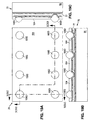
- FIG. 3A A power MOSFET package made by the process of this invention is shown in concept in Figs. 3A-3C .
- package 10 includes a silicon chip 11, in which a power MOSFET (not shown) has been formed by known processes of implantation and diffusion of dopants into the silicon.
- the power MOSFET would often contain an epitaxial layer grown over a silicon substrate, with the active regions of the device being formed in the epitaxial layer.
- a backside support substrate 14 is attached to the back side of chip 11 with a layer of conductive adhesive 13, which could be a conductive epoxy or metal foils.
- the power MOSFET within chip 11 is a vertical device, some of the terminals (e.g., the source and the gate terminals) are located adjacent the front side of the chip 11, and another terminal (e.g., the drain) is located adjacent the back side of the chip 11, electrically connected to the adhesive layer 13.
- a source contact including a source metal layer 12, source pads 15 and source solder bumps 16, is electrically connected to the source terminal.
- Vias 17 extend entirely through the chip 11 and are filled with metal that makes electrical contact with the adhesive layer 13.
- a drain contact, including drain pads 18 and drain solder bumps 19, is electrically connected to the metal in vias 17.
- package 10 can be mounted on a printed circuit board (PCB) or other structure with electrical contact to the drain of power MOSFET being made through solder bumps 19 and electrical contact to the source being made through solder bumps 16.
- PCB printed circuit board
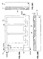
- Fig. 3B shows a bottom view of package 10, showing the section I-I through which Fig. 3A is taken.
- the locations of the drain solder bumps 19 along opposite sides of the package 10 and the source solder bumps 16 in a central region of the chip 11 are shown.
- a gate solder bump 20 at a corner of the chip 11 which makes electrical contact with a gate metal layer within package 10.
- the formation and arrangement of the source and gate metal layers within the package 10 are well known in the art and do not form a part of this invention.
- Fig. 3C is a cross-sectional view of package 10 taken at the section III-III shown in Fig. 3B along the row of drain solder bumps 19.
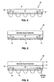
- Figs. 4-6 illustrate several packages.
- Package 40 shown in Fig. 4 omits the backside support substrate 14, and chip 41 would therefore typically be somewhat thicker than chip 11, but otherwise package 40 is similar to package 10 shown in Fig. 1 .
- Vias 41 extend through chip 41 to a layer 43 of conductive material on the back side of chip 41.
- Package 50 shown in Fig. 5 is similar to package 10 but solder balls 16 and 19 are omitted. Package 50 is mounted on a PCB or other structure by making direct connections to source pads 15 and drain pads 18.
- Package 60 shown in Fig. 6 is also similar to package 10, but vias 62 terminate in chip 11 instead of extending entirely through the chip.
- Vias 62 which can be in the form of holes or trenches, terminate in the doped region of the power MOSFET within chip 11 that is adjacent the back side of the chip. For example, for an N-channel MOSFET vias 62 would terminate in the N+ region that forms the drain terminal adjacent the back side of the chip 11.
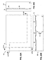
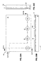
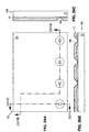
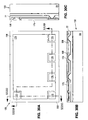
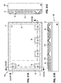
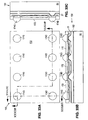
- FIGs. 7A-7C through 20A-20C illustrate a process that may be used to fabricate a package for a power MOSFET in accordance with this invention.
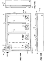
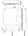
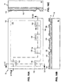
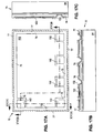
- the figure labeled “A” is a top view of the chip and the figures labeled "B” and “C” are cross-sectional views taken at the sections designated accordingly in the figure labeled "A".
- Figs. 21A to 58C illustrate processes not part of the claimed invention.
- Figs. 7A-7C through 20A-20C illustrate a process sequence which includes forming vias from the front side to the back side of the chip.
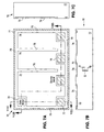
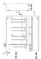
- the initial form of the chip 70 after the power MOSFET and metal contact pads have been formed is shown in Figs. 7A-7C .
- the upper surface of the chip 70 includes a gate contact pad 72 and a source contact pad 74 insulated from each other by a passivation layer 76.
- the gate and source contact pads 72 and 74 are typically made of aluminum, but they could also be made of other metals such as copper or nonmetallic electrically conductive materials.
- a power MOSFET (shown symbolically) is formed in a semiconductor substrate 77, typically silicon. Cross-sectional views taken at sections VIIB-VIIB and VIIC-VIIC, respectively, are shown in Figs. 7B and 7C .
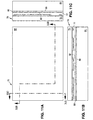
- a substrate 78 is removably attached to the front side of chip 70 with a layer 80 of wax or some other material that allows support substrate 78 to be detached from chip 70 at a later stage. ( Figs. 8A-8C )
- Substrate 77 is thinned by grinding its back side.
- other thinning techniques such as wet etching and vacuum plasma etching can be used to thin substrate 77.
- ADP atmospheric downstream plasma
- substrate 77 can be thinned to a thickness of only 2 mils, for example.
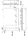
- a barrier layer 82 of Ta/Cu is sputtered on the back side of substrate 77.
- Layer 82 can be 0.5-1.0 ⁇ m thick, for example.
- conductive materials other than Ta/Cu can be used and processes other than sputtering can be used to form the layer. ( Figs. 10A-10C )
- a barrier layer 88 of Ta/Cu is sputtered on a backside substrate 84, and backside substrate 84 is attached to the back side of silicon substrate 77 by means of a layer 86 of solder or another conductive material such as epoxy. ( Figs. 11A-11C )
- Wax layer 80 is heated and support substrate 78 is removed from the front side of silicon substrate 77. ( Figs. 12A-12C )
- a photoresist layer 92 is deposited on the front side of silicon substrate 77. Photoresist layer is patterned and etched to produce openings 94. The etch can be a conventional wet etch process, for example. While openings 94 are circular, they could be any shape. Silicon substrate 77 is etched through openings to form vias 96 and thereby expose the surface of barrier layer 82. As shown, vias 96 are conical in shape because silicon etches along oblique planes. Again, depending on the shape of openings 94, vias 96 could be any shape. As used herein, the word "via” refers to a cavity of any shape whatever that extends partially or entirely through a semiconductor substrate. ( Figs. 13A-13C )
- Photoresist layer 92 is removed exposing vias 96 which extend to the surface of barrier layer 82. ( Figs. 14A-14C )
- a layer 98 of TalCu is sputtered onto the entire surface of chip 70.
- Ta/Cu layer 98 can be 0.5-1.0 ⁇ m thick, for example. ( Figs. 15A-15C )
- a photoresist layer 100 is deposited and patterned, leaving portions of the Ta/Cu layer 98 exposed.
- a copper layer 102 is plated onto the exposed portions of Ta/Cu layer 98. Copper layer 102 generally overlies the gate and source metals and the areas where vias 96 are located. ( Figs. 16A-16C )
- Photoresist layer 100 is removed, leaving the copper layer 102 in place and exposing portions of the silicon substrate 77 and the passivation layer 76. ( Figs. 17A - 17C)
- a passivation layer 104 is patterned over the surface of chip 70 by screen printing, with openings that expose portions of copper layer 102.
- the portion labeled 102G is electrically connected to gate contact pad 72
- portions labeled 102S are electrically connected to source contact pad 74
- portions 102D are electrically connected to solder layer 86, backside substrate 84 and the drain terminal of the power MOSFET. ( Figs. 18A-18C )
- chip 70 and the other chips in the wafer can be labeled with a product or company designation by laser marking the surface of the backside substrate 84.
- Solder bumps 106 are formed over the exposed portions 102G, 102S and 102D of the copper layer 102. Bumps 106G and 106S are electrically connected to the gate and source metal, respectively. Bumps 106D are electrically connected to solder layer 86 and backside substrate 84. ( Figs. 19A-19C )
- Chip 70 is separated from other chips in the wafer by sawing at the locations designated 108.
- the result is a power MOSFET package that can be mounted on a PCB or other structure using flip-chip mounting techniques. ( Figs. 20A-20C )
- Figs. 21A-21 C through 34A-34C illustrate a process sequence which includes forming vias from the back side to the front side of the chip.
- the process begins with a chip 150, shown in Figs. 21A-21C , that is identical to chip 70 shown in Figs. 7A-7C .
- the support substrate 78 is removably attached to the front side of chip 70 with the layer 80 of wax or some other material that allows support substrate 78 to be detached from chip 70 at a later stage. ( Figs. 22A-22C )
- Silicon substrate 77 is thinned by grinding its back side.
- other thinning techniques such as wet etching and vacuum plasma etching can be used to thin substrate 77.
- ADP atmospheric downstream plasma
- substrate 77 can be thinned to a thickness of only 2 mils, for example.
- a photoresist layer 152 is deposited on the back side of the thinned substrate 77. Photoresist layer 152 is patterned and etched to form openings 154. Substrate 77 is etched through openings 154 to form vias 156, with wax layer 80 acting as an etch stop. As shown, vias 156 are conical in shape because silicon etches along oblique planes. Depending on the shape of openings 154, vias 156 could be any shape. ( Figs. 24A - 24C)
- Photoresist layer 152 is removed, leaving vias 156 exposed. ( Figs. 25A-25C )
- Ta/Cu layer 158 can be 0.5-1.0 ⁇ m thick, for example.
- Wax layer 80 is heated and support substrate 78 is removed from the front side of silicon substrate 77. ( Figs. 28A-28C )
- Ta/Cu layer 166 can be 0.5-1.0 ⁇ m thick, for example.
- a photoresist layer 168 is deposited and patterned, leaving portions of the Ta/Cu layer 166 exposed.
- a copper layer 170 is plated onto the exposed portions of Ta/Cu layer 166. Copper layer 170 generally overlies the gate and source metals and the areas where vias 156 are located. ( Figs. 30A-30C )
- Photoresist layer 168 is removed, leaving the copper layer 170 in place and exposing portions of the silicon substrate 77 and the passivation layer 76.
- a passivation layer 172 is patterned over the surface of chip 70 by screen printing, with openings that expose portions of copper layer 170.
- the portion labeled 170G is electrically connected to gate contact pad 72
- portions labeled 170S are electrically connected to source contact pad 74
- portions 170D are electrically connected to solder layer 162, backside substrate 84 and the drain terminal of the power MOSFET. ( Figs. 32A-32C )
- chip 150 and the other chips in the wafer can be labeled with a product or company designation by laser marking the surface of the backside substrate 84.
- Solder bumps 174 are formed over the exposed portions 170G, 170S and 170D of the copper layer 170. Bumps 174G and 174S are electrically connected to the gate and source metal, respectively. Bumps 174D are electrically connected to solder layer 162 and backside substrate 84. ( Figs. 33A-33C )
- Chip 150 is separated from other chips in the wafer by sawing at the locations designated 108.
- the result is a power MOSFET package that can be mounted on a PCB or other structure using flip-chip mounting techniques. ( Figs. 34A-34C )
- vias extend into the drain region but not entirely through the chip.
- Two methods for fabricating packages with this configuration are described below. In both of these methods the resulting package contains vias in the form of trenches that extend into the drain region.
- the first method is described in Figs. 35A-35C to 46A-46C.
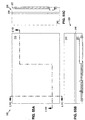
- the initial form of the chip 180 after the power MOSFET and metal contact pads have been formed is shown in Figs. 35A-35C .
- the upper surface of the chip 180 includes a gate contact pad 182, a source contact pad 184 and a passivation layer 186.
- a power MOSFET (shown symbolically) is formed in a semiconductor substrate 187.
- a series of stripes 185 are formed in source contact pad 184, each of stripes 185 containing a central area of substrate 187 surrounded by a border area of passivation layer 186.
- Stripes 185 are formed by the same photolithographic techniques used to pattern the remainder of the surface of chip 180. In place of stripes 185 other geometric shapes could be used to form areas of exposed substrate 187.
- a photoresist layer 192 (e.g., 5 ⁇ m thick) is deposited on the front side of chip 180. Photoresist layer 192 is patterned and etched to produce openings overlying the areas of substrate 187 within the stripes 185. Silicon substrate 187 is etched through the openings in photoresist layer 192 to form trenches 196 in substrate 187. Trenches 196 can be 5 ⁇ m deep. Again, depending on the shape of the openings in photoresist layer 192, circular holes or cavities of other shapes could be formed extending into substrate 187. As stated above, the word "via” is used herein as a generic term referring to trenches, holes or other cavities of any shape whatever that extend partially or entirely through a semiconductor substrate. ( Figs. 36A-36C )
- Photoresist layer 192 is removed and a layer 198 of TalCu is sputtered onto the entire surface of chip 180, including the inside surfaces of trenches 196.
- Ta/Cu layer 198 can be 0.5-1.0 ⁇ m thick, for example. ( Figs. 37A-37C )
- a photoresist layer 200 is deposited and patterned, leaving portions of the Ta/Cu layer 198 exposed.
- a copper layer 202 is plated onto the exposed portions of Ta/Cu layer 198. Copper layer 202 generally overlies the gate and source metals and fills the trenches 196. ( Figs. 38A-38C )
- Photoresist layer 200 is removed, leaving the copper layer 202 in place and exposing portions of Ta/Cu layer 189, the silicon substrate 187 and the passivation layer186. The exposed portions of the Ta/Cu layer 198 are then etched. The copper layer 202 remains in place over the gate contact pad 182 and source contact pad 184, and the portion of copper layer 202 in the trenches also remains in place. ( Figs. 39A - 39C)
- a passivation layer 204 is deposited over the surface of chip 180 and openings are etched in passivation layer 204 to expose portions of copper layer 202.
- the portion labeled 202G is electrically connected to gate contact pad 182
- portions labeled 202S are electrically connected to source contact pad 184
- portions 202D remain in the trenches and extend into the drain region of substrate 187.
- a Ta/Cu layer 205 (e.g., 0.5-1.0 ⁇ m ⁇ m thick) is sputtered over the entire top surface of chip 180. ( Figs. 41A-41C )
- a photoresist layer 206 is deposited on Ta/Cu layer 205 and photolithographically patterned to form apertures 208.
- a Cu layer 210 is plated onto the portions of Ta/Cu layer 205 that are exposed through apertures 208.
- a section 210G is electrically connected to gate contact pad 182, portions labeled 210S are electrically connected to source contact pad 184, and portions 210D are electrically connected to the drain region of substrate 187 via the portions of copper layer 202 that are in trenches 196. ( Figs. 42A-42C )
- Photoresist layer 206 is stripped and Ta/Cu layer 205 is etched, leaving exposed the top surface of passivation layer 204. ( Figs. 43A-43C )
- chip 180 and the other chips in the wafer can be labeled with a product or company designation by laser marking the backside of substrate 187.
- Solder bumps 214 are formed over the exposed portions 210G, 210S and 210D of the copper layer 210. Bumps 214G and 214S are electrically connected to the gate and source metal, respectively. Bumps 214D are electrically connected to the drain region of substrate 187. ( Figs. 45A-45C )
- Chip 180 is separated from other chips in the wafer by sawing at the locations designated 216.
- the result is a power MOSFET package that can be mounted on a PCB or other structure using flip-chip mounting techniques. ( Figs. 46A-46C )
- Figs. 47A-47C The second method of fabricating a package with vias extending part way through the substrate is described in Figs. 47A-47C to 58A-58C.
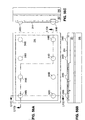
- the initial form of the chip 220 after the power MOSFET and metal contact pads have been formed is shown in Figs. 47A-47C .
- the upper surface of the chip 220 includes a gate contact pad 222, a source contact pad 224 and a passivation layer 226.
- a power MOSFET (shown symbolically) is formed in a semiconductor substrate 227.
- a series of stripes 225 are formed in source contact pad 224, each of stripes 225 containing a central area of substrate 227 bordered by an area of passivation layer 226.
- Stripes 225 are formed by the same photolithographic techniques used to pattern the remainder of the surface of chip 220. In place of stripes 225, other geometric shapes could be used to form areas of exposed substrate 227.
- a photoresist layer 232 (e.g., 5 ⁇ m thick) is deposited on the front side of chip 220. Photoresist layer 232 is patterned and etched to produce openings overlying the areas of substrate 227. ( Figs. 48A-48C )
- Silicon substrate 227 is etched through the openings in photoresist layer 192 to form trenches 236 in substrate 227.
- Trenches 236 can be 5 ⁇ m deep. Again, depending on the shape of the openings in photoresist layer 232, circular holes or cavities of other shapes could be formed extending into substrate 227. As stated above, the word "via” is used herein as a generic term referring to trenches, holes or other cavities of any shape whatever that extend partially or entirely through a semiconductor substrate.
- Photoresist layer 232 is removed, exposing the surface of chip 220. ( Figs. 49A-49C )
- a layer 238 of Ta/Cu is sputtered onto the entire surface of chip 220, including the inside surfaces of trenches 236.
- Ta/Cu layer 238 can 0.5-1.0 ⁇ m thick, for example. ( Figs. 50A-50C )
- a photoresist layer 240 is deposited and patterned, leaving portions of the Ta/Cu layer 238 exposed.
- a copper layer 242 is plated onto the exposed portions of Ta/Cu layer 238. Copper layer 242 generally overlies the gate and source metals and fills the trenches 236. ( Figs. 51A-51C )
- Photoresist layer 240 is removed, leaving the copper layer 242 in place and exposing portions of Ta/Cu layer 238.
- the exposed portions of the Ta/Cu layer 238 are then etched, exposing portions of the silicon substrate 277 and the passivation layer 226.
- the copper layer 242 remains in place over the gate contact pad 222 and source contact pad 224, and the portion of copper layer 242 in the trenches also remains in place. ( Figs. 52A-52C )
- a thick passivation layer 244 is patterned over the surface of chip 220 by screen-printing , with expose portions of copper layer 242 being left exposed.
- the portion labeled 242G is electrically connected to gate contact pad 222
- portions labeled 242S are electrically connected to source contact pad 224
- portions 242D are electrically connected to the drain region of the MOSFET. While openings 241 are shown as circular, other shapes can be used. ( Figs. 53A-53C )
- Substrate 227 is thinned by grinding its back side.
- other thinning techniques such as wet etching and vacuum plasma etching can be used to thin substrate 227.
- ADP atmospheric downstream plasma
- substrate 227 can be thinned to a thickness of only 10 mils, for example.
- a heat sink 245 is bonded to the back side of the thinned substrate 227 using an adhesive layer 246 of, for example, solder or epoxy.
- Heat sink 245 can be a 10 mil thick sheet of copper, for example. ( Figs. 55A-55C )
- chip 220 and the other chips in the wafer can be labeled with a product or company designation by laser marking the backside of substrate 227.
- Solder bumps 248 are formed over the exposed portions 242G, 242S and 242D of the copper layer 242. Bumps 248G and 248S are electrically connected to the gate and source metal, respectively. Bumps 248D are electrically connected to the drain region of substrate 227. ( Figs. 56A-56C )
- Substrate 227 is sawed at the locations designated 250 to separate it from the portions of the substrate in other chips on the wafer.
- the heat sink 245 is left intact. ( Figs. 57A-57C )
- An optional passivation layer 246 is formed on heat sink 245, and chip 220 is separated from other chips in the wafer by sawing through the heat sink 245 at the locations designated 252.
- the result is a power MOSFET package that can be mounted on a PCB or other structure using flip-chip mounting techniques. ( Figs. 58A-58C )
- Figs. 59A and 59B illustrate a diode package the anode being a doped region on the front side of the chip and the cathode being a doped region of opposite conductivity type on the back side of the chip.
- the via that connects the cathode region to the cathode terminal on front side extends all the way through the chip to metal plate that is attached to the back side.
- the via extends only part of the way through the chip into the cathode region.
- Figs. 60A and 60B illustrate a capacitor package, the gate contact being attached to a metal plate that is separated from a heavily-doped silicon region by a nonconductive passivation layer.
- a via connects the heavily-doped region with a back contact on the front side of the chip.
- the via extends all the way through the chip to a metal plate attached to the back side of the chip; in Fig. 60B , the via extends into the heavily-doped region of the chip but does not reach all the way through the chip.
Landscapes
- Internal Circuitry In Semiconductor Integrated Circuit Devices (AREA)
- Electrodes Of Semiconductors (AREA)
Abstract
Description
- This invention relates to wafer-level packaging techniques for semiconductor chips and in particular to packaging techniques for semiconductor chips that contain devices or components, such as vertical power MOSFETs that have terminals on both sides of the chip.
- After the processing of a semiconductor wafer has been completed, the resulting semiconductor chips, which could be integrated circuit (IC) or MOSFET chips for example, must be separated and packaged in such a way that they can be connected to external circuitry. There are many known packaging techniques. Most involve mounting the chip on a leadframe, connecting the chip pads to the leadframe by wire-bonding or otherwise, and then encapsulating the chip and wire bonds in a plastic capsule, with the leadframe left protruding from the capsule. The encapsulation is often done by injection-molding. The leadframe is then trimmed to remove the tie bars that hold it together, and the leads are bent in such a way that the package can be mounted on a flat surface, typically a printed circuit board (PCB).
-
WO 01/59842 DE 19907525 teaches another wafer level chip scale package. Gupta et al. in IEEE Transactions on Electron Devices, vol. ED-30, no. 1, 1983, pp. 16-20, discuss yield considerations for ion-implanted GAAS MMIC's. Chang et al. in IEEE Transactions on Semiconductor Manufacturing, vol. 4, no. 1, pp. 66-68, discuss a hybrid wafer-dicing process for GaAs MMIC production. - This is generally an expensive, time-consuming process, since the individual chips are typically handled separately. Moreover, the resulting semiconductor package is considerably larger than the chip itself, using up an undue amount of scarce "real estate" on the PCB. In addition, wire bonds are fragile and introduce a considerable resistance between the chip pads and the leads of the package.
- The problems are particularly difficult when the device to be packaged is a "vertical" device, having terminals on opposite faces of the chip. For example, a power MOSFET typically has its source and gate terminals on the front side of the chip and its drain terminal on the back side of the chip. Similarly, a vertical diode has its anode terminal on one face of the chip and its cathode terminal on the opposite face of the chip. Bipolar transistors, junction field effect transistors (JFETs), and various types of integrated circuits (ICs) can also be fabricated in a "vertical" configuration, as can passive components components such as semiconductor capacitors or resistors.
- Accordingly, there is a need for a process which is simpler and less expensive than existing processes and which produces a package that is essentially the same size as the chip. There is a particular need for such a process and package that can be used with semiconductor dice having terminals on both their front and back sides. For reasons of economy and enhanced performance, it is desirable that the process be performed on all of the chips in the wafer form before they are separated from each other, i.e., that the process be vertical wafer-level chip-scale packaging.
- The invention is defined in
claim 1. - The invention includes a process of fabricating a power MOSFET package in wafer form, the process comprising the steps of: providing a semiconductor wafer comprising a plurality of chips, each of the chips comprising a power MOSFET, each of the chips having a front side adjacent to which a source region and a gate electrode are located; forming a mask over a front side of the wafer, the mask having a plurality of openings; etching the wafer through the openings in the mask to form a plurality of vias extending through the wafer; depositing metal in the vias; and separating the chips from each other. The process includes the steps of thinning the wafer, for example by grinding or lapping the back side of the wafer, and/or attaching a support substrate to a back side of the wafer. The support substrate can be electrically conductive.
- The process may also include forming solder bumps in the openings for the source, gate and drain pads and insulating the solder bumps by forming a passivation layer.
- The process of this invention can be used to fabricate a package for junction field effect transistors (JFETs).
-
-
Fig. 1 is a cross-sectional view of a conventional vertical trench MOSFET. -
Fig. 2 is a cross-sectional view of a conventional vertical planar DMOSFET. -
Fig. 3A is a general conceptual cross-sectional view of a first embodiment of a semiconductor package. -
Fig. 3B is a bottom view of the package shown inFig. 3A . -
Fig. 3C is another cross-sectional view of the package shown inFig. 3A . -
Fig. 4 is a cross-sectional view of a package without a backside support substrate. -
Fig. 5 is a cross-sectional view of a package with a backside support substrate. -
Fig. 6 is a cross-sectional view of a package wherein the vias extend only part of the way through the semiconductor substrate. -
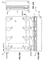
Figs. 7A-7C through 20A-20C illustrate steps of a process of fabricating a package wherein the vias are formed from the front side to the back side of the chip. -
Figs. 21A-21C through 34A-34C illustrate steps of a process of fabricating a package wherein the vias are formed from the back side to the front side of the chip. -
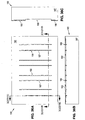
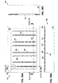
Figs. 35A-35C through 46A-46C illustrate steps of a process of fabricating a package wherein the vias are formed part way through the chip. -
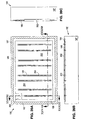
Figs. 47A-47C through 58A-58C illustrate steps of another process of fabricating a package wherein the vias are formed part way through the chip. -
Figs. 59A and 59B are cross-sectional views of diode packages. -
Figs. 60A and 60B are cross-sectional views of capacitor packages. -
Figs. 1 and 2 show cross-sectional views of typical vertical MOSFETs.Fig. 1 shows a trench MOSFET, in which the N+ source regions are located adjacent the trenches at the front side of the chip. A P-body region abuts the N+ source regions along the sides of the trenches, where a channel is formed when the device is conductive. A metal layer on the front side contacts the N+ source regions and the P-body region through a P+ body contact region. An N+ substrate and an N-drift region form the drain region of the MOSFET which is normally contacted by a metal layer at the back side of the chip. The gate is formed in the trenches and controls a flow of current through the channel adjacent the sides of the trenches.Fig. 2 shows a vertical planar double-diffused DMOSFET. The structure is generally similar, but the gate is located over the surface of the chip instead of being in a trench, and controls a flow of current laterally in a channel just below the surface of the P-body regions. Again the drain is located at the back side of the chip. It is important to note that in both devices the drain terminal is located at the back side of the chip and is difficult to access in a package that is to have all terminals on the front side of the chip. (Note: The designations "source" and "drain" are somewhat arbitrary. As used herein, the term "source" refers to the terminal region adjacent the front side of the chip and the term "drain" refers to the terminal region adjacent the back side of the chip.) - A power MOSFET package made by the process of this invention is shown in concept in
Figs. 3A-3C . As shown inFig. 3A ,package 10 includes asilicon chip 11, in which a power MOSFET (not shown) has been formed by known processes of implantation and diffusion of dopants into the silicon. The power MOSFET would often contain an epitaxial layer grown over a silicon substrate, with the active regions of the device being formed in the epitaxial layer. Abackside support substrate 14 is attached to the back side ofchip 11 with a layer of conductive adhesive 13, which could be a conductive epoxy or metal foils. Since the power MOSFET withinchip 11 is a vertical device, some of the terminals (e.g., the source and the gate terminals) are located adjacent the front side of thechip 11, and another terminal (e.g., the drain) is located adjacent the back side of thechip 11, electrically connected to theadhesive layer 13. A source contact, including asource metal layer 12,source pads 15 and source solder bumps 16, is electrically connected to the source terminal.Vias 17 extend entirely through thechip 11 and are filled with metal that makes electrical contact with theadhesive layer 13. A drain contact, includingdrain pads 18 and drain solder bumps 19, is electrically connected to the metal invias 17. - Thus package 10 can be mounted on a printed circuit board (PCB) or other structure with electrical contact to the drain of power MOSFET being made through solder bumps 19 and electrical contact to the source being made through solder bumps 16.
-
Fig. 3B shows a bottom view ofpackage 10, showing the section I-I through whichFig. 3A is taken. The locations of the drain solder bumps 19 along opposite sides of thepackage 10 and the source solder bumps 16 in a central region of thechip 11 are shown. Also shown is agate solder bump 20 at a corner of thechip 11 which makes electrical contact with a gate metal layer withinpackage 10. The formation and arrangement of the source and gate metal layers within thepackage 10 are well known in the art and do not form a part of this invention.Fig. 3C is a cross-sectional view ofpackage 10 taken at the section III-III shown inFig. 3B along the row of drain solder bumps 19. -
Figs. 4-6 illustrate several packages.Package 40 shown inFig. 4 omits thebackside support substrate 14, andchip 41 would therefore typically be somewhat thicker thanchip 11, but otherwisepackage 40 is similar to package 10 shown inFig. 1 .Vias 41 extend throughchip 41 to alayer 43 of conductive material on the back side ofchip 41. -
Package 50 shown inFig. 5 is similar to package 10 butsolder balls Package 50 is mounted on a PCB or other structure by making direct connections to sourcepads 15 anddrain pads 18. -
Package 60 shown inFig. 6 is also similar topackage 10, but vias 62 terminate inchip 11 instead of extending entirely through the chip.Vias 62, which can be in the form of holes or trenches, terminate in the doped region of the power MOSFET withinchip 11 that is adjacent the back side of the chip. For example, for an N-channel MOSFET vias 62 would terminate in the N+ region that forms the drain terminal adjacent the back side of thechip 11. -
Figs. 7A-7C through 20A-20C illustrate a process that may be used to fabricate a package for a power MOSFET in accordance with this invention. In each drawing, the figure labeled "A" is a top view of the chip and the figures labeled "B" and "C" are cross-sectional views taken at the sections designated accordingly in the figure labeled "A". -
Figs. 21A to 58C illustrate processes not part of the claimed invention. -
Figs. 7A-7C through 20A-20C illustrate a process sequence which includes forming vias from the front side to the back side of the chip. The initial form of thechip 70 after the power MOSFET and metal contact pads have been formed is shown inFigs. 7A-7C . As shown in the top view ofFig. 7A , the upper surface of thechip 70 includes agate contact pad 72 and asource contact pad 74 insulated from each other by apassivation layer 76. The gate andsource contact pads semiconductor substrate 77, typically silicon. Cross-sectional views taken at sections VIIB-VIIB and VIIC-VIIC, respectively, are shown inFigs. 7B and 7C . - A
substrate 78 is removably attached to the front side ofchip 70 with alayer 80 of wax or some other material that allowssupport substrate 78 to be detached fromchip 70 at a later stage. (Figs. 8A-8C ) -
Substrate 77 is thinned by grinding its back side. Alternatively, other thinning techniques such as wet etching and vacuum plasma etching can be used tothin substrate 77. Another possibility is the atmospheric downstream plasma (ADP) plasma etching system available from Tru-Si Technologies, Inc. of Sunnyvale, California. In this manner,substrate 77 can be thinned to a thickness of only 2 mils, for example. (Figs. 9A-9C ) - A
barrier layer 82 of Ta/Cu is sputtered on the back side ofsubstrate 77.Layer 82 can be 0.5-1.0 µm thick, for example. Alternatively, conductive materials other than Ta/Cu can be used and processes other than sputtering can be used to form the layer. (Figs. 10A-10C ) - A
barrier layer 88 of Ta/Cu is sputtered on abackside substrate 84, andbackside substrate 84 is attached to the back side ofsilicon substrate 77 by means of alayer 86 of solder or another conductive material such as epoxy. (Figs. 11A-11C ) -
Wax layer 80 is heated andsupport substrate 78 is removed from the front side ofsilicon substrate 77. (Figs. 12A-12C ) - A
photoresist layer 92 is deposited on the front side ofsilicon substrate 77. Photoresist layer is patterned and etched to produceopenings 94. The etch can be a conventional wet etch process, for example. Whileopenings 94 are circular, they could be any shape.Silicon substrate 77 is etched through openings to formvias 96 and thereby expose the surface ofbarrier layer 82. As shown,vias 96 are conical in shape because silicon etches along oblique planes. Again, depending on the shape ofopenings 94, vias 96 could be any shape. As used herein, the word "via" refers to a cavity of any shape whatever that extends partially or entirely through a semiconductor substrate. (Figs. 13A-13C ) -
Photoresist layer 92 is removed exposingvias 96 which extend to the surface ofbarrier layer 82. (Figs. 14A-14C ) - A
layer 98 of TalCu is sputtered onto the entire surface ofchip 70. Ta/Cu layer 98 can be 0.5-1.0 µm thick, for example. (Figs. 15A-15C ) - A
photoresist layer 100 is deposited and patterned, leaving portions of the Ta/Cu layer 98 exposed. Acopper layer 102 is plated onto the exposed portions of Ta/Cu layer 98.Copper layer 102 generally overlies the gate and source metals and the areas wherevias 96 are located. (Figs. 16A-16C ) -
Photoresist layer 100 is removed, leaving thecopper layer 102 in place and exposing portions of thesilicon substrate 77 and thepassivation layer 76. (Figs. 17A -17C) - A
passivation layer 104 is patterned over the surface ofchip 70 by screen printing, with openings that expose portions ofcopper layer 102. The portion labeled 102G is electrically connected togate contact pad 72, portions labeled 102S are electrically connected to sourcecontact pad 74, andportions 102D are electrically connected tosolder layer 86,backside substrate 84 and the drain terminal of the power MOSFET. (Figs. 18A-18C ) - If desired,
chip 70 and the other chips in the wafer can be labeled with a product or company designation by laser marking the surface of thebackside substrate 84. - Solder bumps 106 are formed over the exposed
portions copper layer 102.Bumps Bumps 106D are electrically connected tosolder layer 86 andbackside substrate 84. (Figs. 19A-19C ) -
Chip 70 is separated from other chips in the wafer by sawing at the locations designated 108. The result is a power MOSFET package that can be mounted on a PCB or other structure using flip-chip mounting techniques. (Figs. 20A-20C ) -
Figs. 21A-21C through 34A-34C illustrate a process sequence which includes forming vias from the back side to the front side of the chip. The process begins with achip 150, shown inFigs. 21A-21C , that is identical to chip 70 shown inFigs. 7A-7C . - The
support substrate 78 is removably attached to the front side ofchip 70 with thelayer 80 of wax or some other material that allowssupport substrate 78 to be detached fromchip 70 at a later stage. (Figs. 22A-22C ) -
Silicon substrate 77 is thinned by grinding its back side. Alternatively, other thinning techniques such as wet etching and vacuum plasma etching can be used tothin substrate 77. Another possibility is the atmospheric downstream plasma (ADP) plasma etching system available from Tru-Si Technologies, Inc., of Sunnyvale, California. In this manner,substrate 77 can be thinned to a thickness of only 2 mils, for example. (Figs. 23A-23C ) - A
photoresist layer 152 is deposited on the back side of the thinnedsubstrate 77.Photoresist layer 152 is patterned and etched to formopenings 154.Substrate 77 is etched throughopenings 154 to form vias 156, withwax layer 80 acting as an etch stop. As shown,vias 156 are conical in shape because silicon etches along oblique planes. Depending on the shape ofopenings 154, vias 156 could be any shape. (Figs. 24A -24C) -
Photoresist layer 152 is removed, leavingvias 156 exposed. (Figs. 25A-25C ) - A
layer 158 of Ta/Cu is sputtered onto the back side ofchip 70, extending into thevias 156 and covering thewax layer 80 at the bottom of thevias 156. Ta/Cu layer 158 can be 0.5-1.0 µm thick, for example. (Figs. 26A-26C ) -
Layer 164 of Ta/Cu sputtered on abackside substrate 160, andbackside substrate 160 is attached to the back side ofsilicon substrate 77 by means of alayer 162 of solder or another conductive material such as epoxy.Solder layer 162 fills thevias 156. (Figs. 27A-27C ) -
Wax layer 80 is heated andsupport substrate 78 is removed from the front side ofsilicon substrate 77. (Figs. 28A-28C ) - A
layer 166 of Ta/Cu is sputtered onto the entire surface ofchip 70. Ta/Cu layer 166 can be 0.5-1.0 µm thick, for example. (Figs. 29A-29C ) - A
photoresist layer 168 is deposited and patterned, leaving portions of the Ta/Cu layer 166 exposed. Acopper layer 170 is plated onto the exposed portions of Ta/Cu layer 166.Copper layer 170 generally overlies the gate and source metals and the areas wherevias 156 are located. (Figs. 30A-30C ) -
Photoresist layer 168 is removed, leaving thecopper layer 170 in place and exposing portions of thesilicon substrate 77 and thepassivation layer 76. (31A-31C) - A
passivation layer 172 is patterned over the surface ofchip 70 by screen printing, with openings that expose portions ofcopper layer 170. The portion labeled 170G is electrically connected togate contact pad 72, portions labeled 170S are electrically connected to sourcecontact pad 74, andportions 170D are electrically connected tosolder layer 162,backside substrate 84 and the drain terminal of the power MOSFET. (Figs. 32A-32C ) - If desired,
chip 150 and the other chips in the wafer can be labeled with a product or company designation by laser marking the surface of thebackside substrate 84. - Solder bumps 174 are formed over the exposed
portions copper layer 170.Bumps Bumps 174D are electrically connected tosolder layer 162 andbackside substrate 84. (Figs. 33A-33C ) -
Chip 150 is separated from other chips in the wafer by sawing at the locations designated 108. The result is a power MOSFET package that can be mounted on a PCB or other structure using flip-chip mounting techniques. (Figs. 34A-34C ) - In other packages such as those shown in
Figs. 4, 5 and 6 , vias extend into the drain region but not entirely through the chip. Two methods for fabricating packages with this configuration are described below. In both of these methods the resulting package contains vias in the form of trenches that extend into the drain region. - The first method is described in
Figs. 35A-35C to 46A-46C. The initial form of thechip 180 after the power MOSFET and metal contact pads have been formed is shown inFigs. 35A-35C . As shown in the top view ofFig. 35A , the upper surface of thechip 180 includes agate contact pad 182, asource contact pad 184 and apassivation layer 186. A power MOSFET (shown symbolically) is formed in asemiconductor substrate 187. A series ofstripes 185 are formed insource contact pad 184, each ofstripes 185 containing a central area ofsubstrate 187 surrounded by a border area ofpassivation layer 186.Stripes 185 are formed by the same photolithographic techniques used to pattern the remainder of the surface ofchip 180. In place ofstripes 185 other geometric shapes could be used to form areas of exposedsubstrate 187. - A photoresist layer 192 (e.g., 5 µm thick) is deposited on the front side of
chip 180.Photoresist layer 192 is patterned and etched to produce openings overlying the areas ofsubstrate 187 within thestripes 185.Silicon substrate 187 is etched through the openings inphotoresist layer 192 to formtrenches 196 insubstrate 187.Trenches 196 can be 5 µm deep. Again, depending on the shape of the openings inphotoresist layer 192, circular holes or cavities of other shapes could be formed extending intosubstrate 187. As stated above, the word "via" is used herein as a generic term referring to trenches, holes or other cavities of any shape whatever that extend partially or entirely through a semiconductor substrate. (Figs. 36A-36C ) -
Photoresist layer 192 is removed and alayer 198 of TalCu is sputtered onto the entire surface ofchip 180, including the inside surfaces oftrenches 196. Ta/Cu layer 198 can be 0.5-1.0 µm thick, for example. (Figs. 37A-37C ) - A
photoresist layer 200 is deposited and patterned, leaving portions of the Ta/Cu layer 198 exposed. Acopper layer 202 is plated onto the exposed portions of Ta/Cu layer 198.Copper layer 202 generally overlies the gate and source metals and fills thetrenches 196. (Figs. 38A-38C ) -
Photoresist layer 200 is removed, leaving thecopper layer 202 in place and exposing portions of Ta/Cu layer 189, thesilicon substrate 187 and the passivation layer186. The exposed portions of the Ta/Cu layer 198 are then etched. Thecopper layer 202 remains in place over thegate contact pad 182 andsource contact pad 184, and the portion ofcopper layer 202 in the trenches also remains in place. (Figs. 39A -39C) - A
passivation layer 204 is deposited over the surface ofchip 180 and openings are etched inpassivation layer 204 to expose portions ofcopper layer 202. The portion labeled 202G is electrically connected togate contact pad 182, portions labeled 202S are electrically connected to sourcecontact pad 184, andportions 202D remain in the trenches and extend into the drain region ofsubstrate 187. (Figs. 40A-40C ) - A Ta/Cu layer 205 (e.g., 0.5-1.0 µm µm thick) is sputtered over the entire top surface of
chip 180. (Figs. 41A-41C ) - A
photoresist layer 206 is deposited on Ta/Cu layer 205 and photolithographically patterned to formapertures 208. A Cu layer 210 is plated onto the portions of Ta/Cu layer 205 that are exposed throughapertures 208. Asection 210G is electrically connected togate contact pad 182, portions labeled 210S are electrically connected to sourcecontact pad 184, andportions 210D are electrically connected to the drain region ofsubstrate 187 via the portions ofcopper layer 202 that are intrenches 196. (Figs. 42A-42C ) -
Photoresist layer 206 is stripped and Ta/Cu layer 205 is etched, leaving exposed the top surface ofpassivation layer 204. (Figs. 43A-43C ) - An
epoxy layer 212 deposited on the surface ofpassivation layer 204, and reflowed. This can be done by a screen-printing process to leaveportions Cu layer 205 exposed. - If desired,
chip 180 and the other chips in the wafer can be labeled with a product or company designation by laser marking the backside ofsubstrate 187. - Solder bumps 214 are formed over the exposed
portions Bumps Bumps 214D are electrically connected to the drain region ofsubstrate 187. (Figs. 45A-45C ) -
Chip 180 is separated from other chips in the wafer by sawing at the locations designated 216. The result is a power MOSFET package that can be mounted on a PCB or other structure using flip-chip mounting techniques. (Figs. 46A-46C ) - The second method of fabricating a package with vias extending part way through the substrate is described in
Figs. 47A-47C to 58A-58C. The initial form of thechip 220 after the power MOSFET and metal contact pads have been formed is shown inFigs. 47A-47C . As shown in the top view ofFig. 47A , the upper surface of thechip 220 includes agate contact pad 222, asource contact pad 224 and apassivation layer 226. A power MOSFET (shown symbolically) is formed in asemiconductor substrate 227. A series ofstripes 225 are formed insource contact pad 224, each ofstripes 225 containing a central area ofsubstrate 227 bordered by an area ofpassivation layer 226.Stripes 225 are formed by the same photolithographic techniques used to pattern the remainder of the surface ofchip 220. In place ofstripes 225, other geometric shapes could be used to form areas of exposedsubstrate 227. - A photoresist layer 232 (e.g., 5 µm thick) is deposited on the front side of
chip 220.Photoresist layer 232 is patterned and etched to produce openings overlying the areas ofsubstrate 227. (Figs. 48A-48C ) -
Silicon substrate 227 is etched through the openings inphotoresist layer 192 to formtrenches 236 insubstrate 227.Trenches 236 can be 5 µm deep. Again, depending on the shape of the openings inphotoresist layer 232, circular holes or cavities of other shapes could be formed extending intosubstrate 227. As stated above, the word "via" is used herein as a generic term referring to trenches, holes or other cavities of any shape whatever that extend partially or entirely through a semiconductor substrate.Photoresist layer 232 is removed, exposing the surface ofchip 220. (Figs. 49A-49C ) - A
layer 238 of Ta/Cu is sputtered onto the entire surface ofchip 220, including the inside surfaces oftrenches 236. Ta/Cu layer 238 can 0.5-1.0 µm thick, for example. (Figs. 50A-50C ) - A
photoresist layer 240 is deposited and patterned, leaving portions of the Ta/Cu layer 238 exposed. Acopper layer 242 is plated onto the exposed portions of Ta/Cu layer 238.Copper layer 242 generally overlies the gate and source metals and fills thetrenches 236. (Figs. 51A-51C ) -
Photoresist layer 240 is removed, leaving thecopper layer 242 in place and exposing portions of Ta/Cu layer 238. The exposed portions of the Ta/Cu layer 238 are then etched, exposing portions of the silicon substrate 277 and thepassivation layer 226. Thecopper layer 242 remains in place over thegate contact pad 222 andsource contact pad 224, and the portion ofcopper layer 242 in the trenches also remains in place. (Figs. 52A-52C ) - A
thick passivation layer 244 is patterned over the surface ofchip 220 by screen-printing , with expose portions ofcopper layer 242 being left exposed. The portion labeled 242G is electrically connected togate contact pad 222, portions labeled 242S are electrically connected to sourcecontact pad 224, andportions 242D are electrically connected to the drain region of the MOSFET. Whileopenings 241 are shown as circular, other shapes can be used. (Figs. 53A-53C ) -
Substrate 227 is thinned by grinding its back side. Alternatively, other thinning techniques such as wet etching and vacuum plasma etching can be used tothin substrate 227. Another possibility is the atmospheric downstream plasma (ADP) plasma etching system available from Tru-Si Technologies, Inc. In this manner,substrate 227 can be thinned to a thickness of only 10 mils, for example. (Figs. 54A-54C ) - A
heat sink 245 is bonded to the back side of the thinnedsubstrate 227 using anadhesive layer 246 of, for example, solder or epoxy.Heat sink 245 can be a 10 mil thick sheet of copper, for example. (Figs. 55A-55C ) - If desired,
chip 220 and the other chips in the wafer can be labeled with a product or company designation by laser marking the backside ofsubstrate 227. - Solder bumps 248 are formed over the exposed
portions copper layer 242.Bumps Bumps 248D are electrically connected to the drain region ofsubstrate 227. (Figs. 56A-56C ) -
Substrate 227 is sawed at the locations designated 250 to separate it from the portions of the substrate in other chips on the wafer. Theheat sink 245 is left intact. (Figs. 57A-57C ) - An
optional passivation layer 246 is formed onheat sink 245, andchip 220 is separated from other chips in the wafer by sawing through theheat sink 245 at the locations designated 252. The result is a power MOSFET package that can be mounted on a PCB or other structure using flip-chip mounting techniques. (Figs. 58A-58C ) -
Figs. 59A and 59B illustrate a diode package the anode being a doped region on the front side of the chip and the cathode being a doped region of opposite conductivity type on the back side of the chip. InFig. 59A , the via that connects the cathode region to the cathode terminal on front side extends all the way through the chip to metal plate that is attached to the back side. InFig. 59B , the via extends only part of the way through the chip into the cathode region. -
Figs. 60A and 60B illustrate a capacitor package, the gate contact being attached to a metal plate that is separated from a heavily-doped silicon region by a nonconductive passivation layer. A via connects the heavily-doped region with a back contact on the front side of the chip. InFig. 60A , the via extends all the way through the chip to a metal plate attached to the back side of the chip; inFig. 60B , the via extends into the heavily-doped region of the chip but does not reach all the way through the chip. - While specific embodiments of this invention have been described, it will be apparent to those skilled in the art that numerous alternative embodiments may be fabricated in accordance with the broad principles of this invention. For example, while the embodiments above relate to N-channel MOSFETs, this invention is also applicable to P-channel MOSFETs. While the conductive material in the vias and elsewhere has been described as a metal, other types of conductive materials such as polysilicon can be used in some embodiments. These and other variations are included within the scope of this invention.
Claims (7)
- A process of fabricating a power MOSFET package or a JFET package the process comprising:providing a semiconductor wafer comprising a plurality of chips (70), each of the chips (70) comprising a power MOSFET or JFET, the wafer having first and second principal surfaces, each power MOSFET or JFET having at least one gate contact pad (72) and at least one source contact pad (74) on the first principal surface, and a drain region;removably attaching a first support substrate (78) to an attaching layer (80) on the first principal surface;thinning the semiconductor wafer from the second principal surface; such that the drain region is located adjacent the second principal surface; depositing a conductive barrier layer (82) on the second principal surface;attaching a second support substrate (84, 88, 86) to the conductive barrier layer (82) on the second principal surface;removing the attaching layer (80) and the first support substrate (78) from the first principal surface;forming a mask (92) over the first principal surface of the wafer, the mask having a plurality of openings (94), there being at least one opening over each of the chips;etching the wafer through the openings (94) in the mask (92) to expose the conductive barrier layer (82) of the second principal surface to form a plurality of vias (96);removing the mask (92);depositing an electrically conductive material (98, 102) in the vias (96) such that the electrically conductive material (98, 102) electrically couples to the drain region of the wafer; andseparating the chips (70) from each other.
- The process of Claim 1 wherein thinning the wafer comprises grinding or lapping the wafer.
- The process of Claim 1 wherein thinning the wafer comprises etching the wafer.
- The process of Claim 1 wherein depositing an electrically conductive material comprises depositing a metal.
- The process of Claim 4 wherein depositing a metal comprises electrolytic plating
- The process of Claim 5 wherein depositing metal in the vias comprises forming a second mask layer having openings coinciding with the locations of the vias.
- The process of Claim 5 wherein depositing metal in the vias comprises sputtering a first metal layer (98) on the first principal surface of the wafer prior to electrolytic plating.
Applications Claiming Priority (3)
| Application Number | Priority Date | Filing Date | Title |
|---|---|---|---|
| US09/545,287 US6392290B1 (en) | 2000-04-07 | 2000-04-07 | Vertical structure for semiconductor wafer-level chip scale packages |
| US545287 | 2000-04-07 | ||
| PCT/US2001/011324 WO2001078144A1 (en) | 2000-04-07 | 2001-04-06 | Vertical structure and process for semiconductor wafer-level chip scale packages |
Publications (2)
| Publication Number | Publication Date |
|---|---|
| EP1273039A1 EP1273039A1 (en) | 2003-01-08 |
| EP1273039B1 true EP1273039B1 (en) | 2009-09-16 |
Family
ID=24175621
Family Applications (1)
| Application Number | Title | Priority Date | Filing Date |
|---|---|---|---|
| EP01924799A Expired - Lifetime EP1273039B1 (en) | 2000-04-07 | 2001-04-06 | Process for semiconductor wafer-level chip scale packages |
Country Status (6)
| Country | Link |
|---|---|
| US (1) | US6392290B1 (en) |
| EP (1) | EP1273039B1 (en) |
| JP (1) | JP4828075B2 (en) |
| AU (1) | AU2001251418A1 (en) |
| DE (2) | DE1273039T1 (en) |
| WO (1) | WO2001078144A1 (en) |
Families Citing this family (77)
| Publication number | Priority date | Publication date | Assignee | Title |
|---|---|---|---|---|
| US7211877B1 (en) * | 1999-09-13 | 2007-05-01 | Vishay-Siliconix | Chip scale surface mount package for semiconductor device and process of fabricating the same |
| CN1315195C (en) * | 2000-02-10 | 2007-05-09 | 国际整流器有限公司 | Vertical conductive flip-chip device with bulk connection on one side |
| US7151036B1 (en) * | 2002-07-29 | 2006-12-19 | Vishay-Siliconix | Precision high-frequency capacitor formed on semiconductor substrate |
| US7132712B2 (en) | 2002-11-05 | 2006-11-07 | Fairchild Semiconductor Corporation | Trench structure having one or more diodes embedded therein adjacent a PN junction |
| US6645791B2 (en) | 2001-04-23 | 2003-11-11 | Fairchild Semiconductor | Semiconductor die package including carrier with mask |
| US20020173077A1 (en) * | 2001-05-03 | 2002-11-21 | Ho Tzong Da | Thermally enhanced wafer-level chip scale package and method of fabricating the same |
| US7061066B2 (en) | 2001-10-17 | 2006-06-13 | Fairchild Semiconductor Corporation | Schottky diode using charge balance structure |
| US6947234B2 (en) * | 2002-07-23 | 2005-09-20 | International Business Machines Corporation | Method, system, and program for performing error correction in a storage device having a magnetic storage medium |
| US6667191B1 (en) * | 2002-08-05 | 2003-12-23 | Asat Ltd. | Chip scale integrated circuit package |
| US7045884B2 (en) * | 2002-10-04 | 2006-05-16 | International Rectifier Corporation | Semiconductor device package |
| TWI227050B (en) * | 2002-10-11 | 2005-01-21 | Sanyo Electric Co | Semiconductor device and method for manufacturing the same |
| US6969909B2 (en) | 2002-12-20 | 2005-11-29 | Vlt, Inc. | Flip chip FET device |
| US7038917B2 (en) * | 2002-12-27 | 2006-05-02 | Vlt, Inc. | Low loss, high density array interconnection |
| US7217594B2 (en) * | 2003-02-11 | 2007-05-15 | Fairchild Semiconductor Corporation | Alternative flip chip in leaded molded package design and method for manufacture |
| JP4130158B2 (en) * | 2003-06-09 | 2008-08-06 | 三洋電機株式会社 | Semiconductor device manufacturing method, semiconductor device |
| EP1482553A3 (en) * | 2003-05-26 | 2007-03-28 | Sanyo Electric Co., Ltd. | Semiconductor device and manufacturing method thereof |
| DE10345494B4 (en) * | 2003-09-30 | 2016-04-07 | Infineon Technologies Ag | Method for processing a thin semiconductor substrate |
| JP3929966B2 (en) * | 2003-11-25 | 2007-06-13 | 新光電気工業株式会社 | Semiconductor device and manufacturing method thereof |
| US7217988B2 (en) * | 2004-06-04 | 2007-05-15 | International Business Machines Corporation | Bipolar transistor with isolation and direct contacts |
| FR2874127B1 (en) * | 2004-08-03 | 2006-12-08 | United Monolithic Semiconduct | MINIATURE MICROFREQUENCY CASE FOR SURFACE MOUNTING AND METHOD FOR MANUFACTURING THE HOUSING |
| US7352036B2 (en) | 2004-08-03 | 2008-04-01 | Fairchild Semiconductor Corporation | Semiconductor power device having a top-side drain using a sinker trench |
| JP4153932B2 (en) * | 2004-09-24 | 2008-09-24 | 株式会社東芝 | Semiconductor device and manufacturing method of semiconductor device |
| WO2006108011A2 (en) | 2005-04-06 | 2006-10-12 | Fairchild Semiconductor Corporation | Trenched-gate field effect transistors and methods of forming the same |
| JP2006352008A (en) * | 2005-06-20 | 2006-12-28 | Nec Electronics Corp | Semiconductor device and circuit board |
| US7635637B2 (en) * | 2005-07-25 | 2009-12-22 | Fairchild Semiconductor Corporation | Semiconductor structures formed on substrates and methods of manufacturing the same |
| DE102005053842B4 (en) * | 2005-11-09 | 2008-02-07 | Infineon Technologies Ag | Semiconductor device with connecting elements and method for producing the same |
| JP2007184553A (en) * | 2005-12-06 | 2007-07-19 | Sanyo Electric Co Ltd | Semiconductor device and manufacturing method thereof |
| US20070158796A1 (en) * | 2005-12-09 | 2007-07-12 | International Rectifier Corporation | Semiconductor package |
| DE102006012739B3 (en) * | 2006-03-17 | 2007-11-08 | Infineon Technologies Ag | Power transistor and power semiconductor device |
| US7446374B2 (en) | 2006-03-24 | 2008-11-04 | Fairchild Semiconductor Corporation | High density trench FET with integrated Schottky diode and method of manufacture |
| US7635635B2 (en) * | 2006-04-06 | 2009-12-22 | Fairchild Semiconductor Corporation | Method for bonding a semiconductor substrate to a metal substrate |
| US7768075B2 (en) | 2006-04-06 | 2010-08-03 | Fairchild Semiconductor Corporation | Semiconductor die packages using thin dies and metal substrates |
| KR100691632B1 (en) | 2006-05-16 | 2007-03-12 | 삼성전기주식회사 | Semiconductor chip, manufacturing method of semiconductor chip and semiconductor chip package |
| US7285477B1 (en) | 2006-05-16 | 2007-10-23 | International Business Machines Corporation | Dual wired integrated circuit chips |
| JP5141076B2 (en) * | 2006-06-05 | 2013-02-13 | 株式会社デンソー | Semiconductor device |
| DE102006033319B4 (en) * | 2006-07-17 | 2010-09-30 | Infineon Technologies Ag | Method for producing a semiconductor device in semiconductor chip size with a semiconductor chip |
| US7982309B2 (en) * | 2007-02-13 | 2011-07-19 | Infineon Technologies Ag | Integrated circuit including gas phase deposited packaging material |
| US7482645B2 (en) * | 2007-03-30 | 2009-01-27 | Fairchild Semiconductor Corporation | Method and structure for making a top-side contact to a substrate |
| US8217511B2 (en) * | 2007-07-31 | 2012-07-10 | Freescale Semiconductor, Inc. | Redistributed chip packaging with thermal contact to device backside |
| US20090032871A1 (en) * | 2007-08-01 | 2009-02-05 | Louis Vervoort | Integrated circuit with interconnected frontside contact and backside contact |
| US8101500B2 (en) | 2007-09-27 | 2012-01-24 | Fairchild Semiconductor Corporation | Semiconductor device with (110)-oriented silicon |
| US7884390B2 (en) * | 2007-10-02 | 2011-02-08 | Fairchild Semiconductor Corporation | Structure and method of forming a topside contact to a backside terminal of a semiconductor device |
| US20090127677A1 (en) * | 2007-11-21 | 2009-05-21 | Gomez Jocel P | Multi-Terminal Package Assembly For Semiconductor Devices |
| US20090137097A1 (en) * | 2007-11-26 | 2009-05-28 | United Microelectronics Corp. | Method for dicing wafer |
| US7910992B2 (en) * | 2008-07-15 | 2011-03-22 | Maxim Integrated Products, Inc. | Vertical MOSFET with through-body via for gate |
| JP5313601B2 (en) * | 2008-07-17 | 2013-10-09 | ローム株式会社 | Semiconductor device unit |
| US8039877B2 (en) * | 2008-09-09 | 2011-10-18 | Fairchild Semiconductor Corporation | (110)-oriented p-channel trench MOSFET having high-K gate dielectric |
| US8710665B2 (en) | 2008-10-06 | 2014-04-29 | Infineon Technologies Ag | Electronic component, a semiconductor wafer and a method for producing an electronic component |
| US8058732B2 (en) * | 2008-11-20 | 2011-11-15 | Fairchild Semiconductor Corporation | Semiconductor die structures for wafer-level chipscale packaging of power devices, packages and systems for using the same, and methods of making the same |
| US8174067B2 (en) * | 2008-12-08 | 2012-05-08 | Fairchild Semiconductor Corporation | Trench-based power semiconductor devices with increased breakdown voltage characteristics |
| US8304829B2 (en) * | 2008-12-08 | 2012-11-06 | Fairchild Semiconductor Corporation | Trench-based power semiconductor devices with increased breakdown voltage characteristics |
| US7960800B2 (en) * | 2008-12-12 | 2011-06-14 | Fairchild Semiconductor Corporation | Semiconductor dice with backside trenches filled with elastic material for improved attachment, packages using the same, and methods of making the same |
| US8227855B2 (en) * | 2009-02-09 | 2012-07-24 | Fairchild Semiconductor Corporation | Semiconductor devices with stable and controlled avalanche characteristics and methods of fabricating the same |
| US8148749B2 (en) * | 2009-02-19 | 2012-04-03 | Fairchild Semiconductor Corporation | Trench-shielded semiconductor device |
| US8323996B2 (en) * | 2009-03-02 | 2012-12-04 | Infineon Technologies Ag | Semiconductor device |
| US8174131B2 (en) * | 2009-05-27 | 2012-05-08 | Globalfoundries Inc. | Semiconductor device having a filled trench structure and methods for fabricating the same |
| US8563360B2 (en) * | 2009-06-08 | 2013-10-22 | Alpha And Omega Semiconductor, Inc. | Power semiconductor device package and fabrication method |
| US8049276B2 (en) | 2009-06-12 | 2011-11-01 | Fairchild Semiconductor Corporation | Reduced process sensitivity of electrode-semiconductor rectifiers |
| US20110147796A1 (en) * | 2009-12-17 | 2011-06-23 | Infineon Technologies Austria Ag | Semiconductor device with metal carrier and manufacturing method |
| US8487371B2 (en) | 2011-03-29 | 2013-07-16 | Fairchild Semiconductor Corporation | Vertical MOSFET transistor having source/drain contacts disposed on the same side and method for manufacturing the same |
| US8791015B2 (en) | 2011-04-30 | 2014-07-29 | Stats Chippac, Ltd. | Semiconductor device and method of forming shielding layer over active surface of semiconductor die |
| US20160247879A1 (en) * | 2015-02-23 | 2016-08-25 | Polar Semiconductor, Llc | Trench semiconductor device layout configurations |
| TWI690083B (en) * | 2015-04-15 | 2020-04-01 | 杰力科技股份有限公司 | Power mosfet and manufacturing method thereof |
| KR102163602B1 (en) * | 2017-07-13 | 2020-10-12 | 매그나칩 반도체 유한회사 | Semiconductor Device with Stacking Structure of Silicon-Conductor layer-Silicon |
| US10991660B2 (en) * | 2017-12-20 | 2021-04-27 | Alpha Anc Omega Semiconductor (Cayman) Ltd. | Semiconductor package having high mechanical strength |
| CN109473362B (en) * | 2018-10-29 | 2020-04-21 | 上海朕芯微电子科技有限公司 | A CSP packaging method for power devices |
| IT201900006736A1 (en) | 2019-05-10 | 2020-11-10 | Applied Materials Inc | PACKAGE MANUFACTURING PROCEDURES |
| IT201900006740A1 (en) * | 2019-05-10 | 2020-11-10 | Applied Materials Inc | SUBSTRATE STRUCTURING PROCEDURES |
| EP3761357A1 (en) * | 2019-07-04 | 2021-01-06 | Infineon Technologies Austria AG | Semiconductor device |
| US11862546B2 (en) | 2019-11-27 | 2024-01-02 | Applied Materials, Inc. | Package core assembly and fabrication methods |
| CN114982078B (en) * | 2020-01-13 | 2023-04-28 | 新唐科技日本株式会社 | Semiconductor device with a semiconductor device having a plurality of semiconductor chips |
| US11257790B2 (en) | 2020-03-10 | 2022-02-22 | Applied Materials, Inc. | High connectivity device stacking |
| US11454884B2 (en) | 2020-04-15 | 2022-09-27 | Applied Materials, Inc. | Fluoropolymer stamp fabrication method |
| US11676832B2 (en) | 2020-07-24 | 2023-06-13 | Applied Materials, Inc. | Laser ablation system for package fabrication |
| US11404318B2 (en) | 2020-11-20 | 2022-08-02 | Applied Materials, Inc. | Methods of forming through-silicon vias in substrates for advanced packaging |
| CN114695301A (en) * | 2020-12-30 | 2022-07-01 | 万国半导体国际有限合伙公司 | Semiconductor package having thin substrate and method of manufacturing the same |
| CN114944340B (en) * | 2022-05-03 | 2025-09-09 | 上海韦尔半导体股份有限公司 | Chip packaging technology and chip |
Citations (1)
| Publication number | Priority date | Publication date | Assignee | Title |
|---|---|---|---|---|
| WO2001059842A1 (en) * | 2000-02-10 | 2001-08-16 | International Rectifier Corporation | Vertical conduction flip-chip device with bump contacts on single surface |
Family Cites Families (12)
| Publication number | Priority date | Publication date | Assignee | Title |
|---|---|---|---|---|
| JPS61131435A (en) * | 1984-11-30 | 1986-06-19 | Toshiba Corp | Semiconductor device |
| US5103290A (en) * | 1989-06-16 | 1992-04-07 | General Electric Company | Hermetic package having a lead extending through an aperture in the package lid and packaged semiconductor chip |
| JP2713113B2 (en) * | 1993-08-17 | 1998-02-16 | 日本電気株式会社 | Method for manufacturing semiconductor device |
| DE19543540C1 (en) * | 1995-11-22 | 1996-11-21 | Siemens Ag | Vertically integrated semiconductor component |
| US6020637A (en) * | 1997-05-07 | 2000-02-01 | Signetics Kp Co., Ltd. | Ball grid array semiconductor package |
| JP4147596B2 (en) | 1997-06-20 | 2008-09-10 | 東洋紡績株式会社 | Incubator and analyzer equipped with the same |
| JP2868008B1 (en) * | 1997-11-21 | 1999-03-10 | 日本電気株式会社 | Semiconductor device and manufacturing method thereof |
| DE69737262T2 (en) | 1997-11-26 | 2007-11-08 | Stmicroelectronics S.R.L., Agrate Brianza | A method of manufacturing a front-to-back via in micro-integrated circuits |
| JP3447941B2 (en) * | 1998-01-05 | 2003-09-16 | 株式会社東芝 | Semiconductor device and manufacturing method thereof |
| US6075290A (en) | 1998-02-26 | 2000-06-13 | National Semiconductor Corporation | Surface mount die: wafer level chip-scale package and process for making the same |
| US6048772A (en) | 1998-05-04 | 2000-04-11 | Xemod, Inc. | Method for fabricating a lateral RF MOS device with an non-diffusion source-backside connection |
| EP1151476B1 (en) * | 1999-11-11 | 2008-04-16 | Nxp B.V. | Semiconductor device having a field effect transistor and a method of manufacturing such a device |
-
2000
- 2000-04-07 US US09/545,287 patent/US6392290B1/en not_active Expired - Lifetime
-
2001
- 2001-04-06 DE DE1273039T patent/DE1273039T1/en active Pending
- 2001-04-06 JP JP2001574900A patent/JP4828075B2/en not_active Expired - Lifetime
- 2001-04-06 DE DE60139927T patent/DE60139927D1/en not_active Expired - Lifetime
- 2001-04-06 WO PCT/US2001/011324 patent/WO2001078144A1/en not_active Ceased
- 2001-04-06 AU AU2001251418A patent/AU2001251418A1/en not_active Abandoned
- 2001-04-06 EP EP01924799A patent/EP1273039B1/en not_active Expired - Lifetime
Patent Citations (1)
| Publication number | Priority date | Publication date | Assignee | Title |
|---|---|---|---|---|
| WO2001059842A1 (en) * | 2000-02-10 | 2001-08-16 | International Rectifier Corporation | Vertical conduction flip-chip device with bump contacts on single surface |
Also Published As
| Publication number | Publication date |
|---|---|
| JP4828075B2 (en) | 2011-11-30 |
| DE60139927D1 (en) | 2009-10-29 |
| US6392290B1 (en) | 2002-05-21 |
| WO2001078144A1 (en) | 2001-10-18 |
| AU2001251418A1 (en) | 2001-10-23 |
| EP1273039A1 (en) | 2003-01-08 |
| JP2003530695A (en) | 2003-10-14 |
| DE1273039T1 (en) | 2003-08-14 |
Similar Documents
| Publication | Publication Date | Title |
|---|---|---|
| US6392290B1 (en) | Vertical structure for semiconductor wafer-level chip scale packages | |
| US6867489B1 (en) | Semiconductor die package processable at the wafer level | |
| KR100737204B1 (en) | Manufacturing Method of Semiconductor Device | |
| US6830959B2 (en) | Semiconductor die package with semiconductor die having side electrical connection | |
| CN101904004B (en) | Wafer level chip scale package and process of manufacture | |
| JP4878030B2 (en) | Re-dispersed solder pads using etched lead frames | |
| US12087717B2 (en) | Semiconductor package and methods of manufacturing a semiconductor package | |
| US20110018116A1 (en) | Chip scale surface mounted semiconductor device package and process of manufacture | |
| US20070045785A1 (en) | Reversible-multiple footprint package and method of manufacturing | |
| US8723300B2 (en) | Multi-chip module power clip | |
| JP2005332999A (en) | CIRCUIT DEVICE, ITS MANUFACTURING METHOD, AND PLATE | |
| JP4094075B2 (en) | Module package without wire bond and manufacturing method | |
| CN108807197B (en) | Chip package with sidewall metallization | |
| US5444009A (en) | Fabricating a semiconductor with an insulative coating | |
| KR100357803B1 (en) | Method of fabricating multi-chip packages | |
| KR100738149B1 (en) | Semiconductor device and manufacturing method thereof | |
| US5521420A (en) | Fabricating a semiconductor with an insulative coating | |
| US12622279B2 (en) | Package with dual layer routing including ground return path | |
| US11721654B2 (en) | Ultra-thin multichip power devices | |
| CN112185931B (en) | semiconductor devices | |
| JP2003124222A (en) | Semiconductor device | |
| US6787871B2 (en) | Integrated schottky barrier diode and manufacturing method thereof | |
| US20240429140A1 (en) | Semiconductor package having multiple redistribution layers and method of making the same | |
| US20260114297A1 (en) | Integrated circuit chip package that does not utilize a leadframe | |
| JP2000100864A (en) | Semiconductor device and its assembly |
Legal Events
| Date | Code | Title | Description |
|---|---|---|---|
| PUAI | Public reference made under article 153(3) epc to a published international application that has entered the european phase |
Free format text: ORIGINAL CODE: 0009012 |
|
| 17P | Request for examination filed |
Effective date: 20021106 |
|
| AK | Designated contracting states |
Kind code of ref document: A1 Designated state(s): AT BE CH CY DE DK ES FI FR GB GR IE IT LI LU MC NL PT SE TR |
|
| AX | Request for extension of the european patent |
Free format text: AL;LT;LV;MK;RO;SI |
|
| EL | Fr: translation of claims filed | ||
| DET | De: translation of patent claims | ||
| 17Q | First examination report despatched |
Effective date: 20020804 |
|
| RBV | Designated contracting states (corrected) |
Designated state(s): DE FR |
|
| GRAP | Despatch of communication of intention to grant a patent |
Free format text: ORIGINAL CODE: EPIDOSNIGR1 |
|
| RIC1 | Information provided on ipc code assigned before grant |
Ipc: H01L 21/768 20060101AFI20090401BHEP |
|
| RTI1 | Title (correction) |
Free format text: PROCESS FOR SEMICONDUCTOR WAFER-LEVEL CHIP SCALE PACKAGES |
|
| GRAS | Grant fee paid |
Free format text: ORIGINAL CODE: EPIDOSNIGR3 |
|
| GRAA | (expected) grant |
Free format text: ORIGINAL CODE: 0009210 |
|
| AK | Designated contracting states |
Kind code of ref document: B1 Designated state(s): DE FR |
|
| REF | Corresponds to: |
Ref document number: 60139927 Country of ref document: DE Date of ref document: 20091029 Kind code of ref document: P |
|
| PLBE | No opposition filed within time limit |
Free format text: ORIGINAL CODE: 0009261 |
|
| STAA | Information on the status of an ep patent application or granted ep patent |
Free format text: STATUS: NO OPPOSITION FILED WITHIN TIME LIMIT |
|
| 26N | No opposition filed |
Effective date: 20100617 |
|
| REG | Reference to a national code |
Ref country code: FR Ref legal event code: PLFP Year of fee payment: 16 |
|
| REG | Reference to a national code |
Ref country code: FR Ref legal event code: PLFP Year of fee payment: 17 |
|
| REG | Reference to a national code |
Ref country code: FR Ref legal event code: PLFP Year of fee payment: 18 |
|
| PGFP | Annual fee paid to national office [announced via postgrant information from national office to epo] |
Ref country code: DE Payment date: 20200429 Year of fee payment: 20 Ref country code: FR Payment date: 20200427 Year of fee payment: 20 |
|
| REG | Reference to a national code |
Ref country code: DE Ref legal event code: R071 Ref document number: 60139927 Country of ref document: DE |