EP1271777A1 - A digital technologic attenuate control circuit of current-model step by step - Google Patents
A digital technologic attenuate control circuit of current-model step by step Download PDFInfo
- Publication number
- EP1271777A1 EP1271777A1 EP01905585A EP01905585A EP1271777A1 EP 1271777 A1 EP1271777 A1 EP 1271777A1 EP 01905585 A EP01905585 A EP 01905585A EP 01905585 A EP01905585 A EP 01905585A EP 1271777 A1 EP1271777 A1 EP 1271777A1
- Authority
- EP
- European Patent Office
- Prior art keywords
- mos transistor
- current
- input
- drain
- mos
- Prior art date
- Legal status (The legal status is an assumption and is not a legal conclusion. Google has not performed a legal analysis and makes no representation as to the accuracy of the status listed.)
- Granted
Links
Images




Classifications
-
- H—ELECTRICITY
- H03—ELECTRONIC CIRCUITRY
- H03G—CONTROL OF AMPLIFICATION
- H03G1/00—Details of arrangements for controlling amplification
- H03G1/0005—Circuits characterised by the type of controlling devices operated by a controlling current or voltage signal
- H03G1/0088—Circuits characterised by the type of controlling devices operated by a controlling current or voltage signal using discontinuously variable devices, e.g. switch-operated
-
- H—ELECTRICITY
- H03—ELECTRONIC CIRCUITRY
- H03H—IMPEDANCE NETWORKS, e.g. RESONANT CIRCUITS; RESONATORS
- H03H11/00—Networks using active elements
- H03H11/02—Multiple-port networks
- H03H11/24—Frequency-independent attenuators
Definitions
- the present invention relates generally to an interface integrated circuit for data communication, and more particularly to a current mode step attenuation control circuit with digital technology.
- Voltage attenuation control has an important role in signal processing circuit with Digital Signal Process (DSP) as a kernel.
- DSP Digital Signal Process
- amplitude limit distortion will be lowered and accuracy of signal processing will be raised.
- signal output when signal amplitude is too large, attenuation will lower interference to adjacent channel and raise the whole system performance.
- a conventional voltage attenuation circuit is consisted of one operational amplifier and two variable resistors, wherein V in is an input voltage signal, V bias is a DC bias voltage, V out is an output voltage signal and variable resistors R1 and R2 are used to adjust gain.
- output voltage has a linear relationship with resistance ratio of variable resistors R1 and R2, but the polarity is opposite to the input signal.
- step voltage attenuation control can be implemented.
- changing R2 resistance is an easier way to attenuate by digital signal control, but when attenuation amplitude is large, connected larger resistance R2 will cause larger noise.
- this attenuation circuit which is consisted of resistors, some elements, such as MOS switch etc., work at nonlinear zone and there are conducting resistances, so the attenuation circuit must have larger resistance of R2, otherwise control accuracy is worse. As there are larger resistances, the attenuation circuit cannot be integrated by standard digital integrated circuit technology.
- FIG. 2 shows a step attenuation circuit controlled by 5bits digital signal.
- V inP and V inN are two complement input voltage signals
- V outP and V outN are two complement output voltage signals too
- b0 ⁇ b4 are five levels digital signal for step attenuation control.
- the 2 to 4 decoder decodes 2 Most Signification Bits (2MSB) of the digital signal.
- the outputs of 2 to 4 decoder are IN0 ⁇ IN3 which control cut-in or cut-off of full differential operational amplifier input switches: SW1P and SW1N, SW2P and SW2N, SW3P and SW3N, SW4P and SW4N, respectively.
- the 3 to 8 decoder decodes 3 Lowest Signification Bits (3LSB) of the digital signal.
- the outputs of 3 to 8 decoder are OUT0, OUT1, ... ... OUT7 which control cut-in and cut-off of full differential operational amplifier output switches: SWO1P and SWO1N, SWO2P and SWO2N, ... ... , SWO7P and SWO7N, SWO8P and SWO8N, respectively.
- the VDC is a needed DC component of output differential signal
- CMFB in is the input of CMFB
- CMFB out is the output of CMFB.
- the voltage attenuation control in circuit above is in segment, i.e. with 2MSB decoder, the control is divided into four segments and each 8DB is a control segment.
- n is a decimal number corresponding to 3LSB of a binary digital control signal.
- a calculated number n is used in attenuation calculation formulas to sum the corresponding cut in resistances in numerator and denominator.
- MOS switch has a conducting resistance, said above, when considering switch conducting resistance, control accuracy of voltage attenuation will be affected. Taking 0DB attenuation as an example, after considering the conducting resistance effect of MOS switch, a real attenuation is
- numerator is a total output resistance of cut in circuits and denominator is a total input resistance of cut in circuits.
- the attenuation calculating formula is similar as above, the only difference is by considering the MOS switch conducting resistance effect in the acting on input circuit resistance. When an output switch is also cut in the circuit, switch conducting resistance effect is also considered in corresponding numerator items. Because, at output, switches are parallel cut in, at most only one switch conducting resistance effect is considered, but, at input, switches are serially cut in, so at most it should consider conducting resistance effect for three switches.
- Attenuation can be gradually increased in an equal step length for DB value, but for resistance of a cut-in circuit corresponding to the increasing DB value, the resistance is increased in an irregular way. Consequently, for twelve resistances in a cut-in circuit, each one has a different increased resistance.
- resistance match if ratio of two matched resistances is a integer, especially 1, 2, 4, 8, ..., the match performance are best. Therefore, for resistances match in a circuit, if there is a resistance match with non- integer proportional relationship, then implementation of layout is very difficult.
- Table 1 shows relationship between DB attenuation and real attenuation multiple.
- the invention provides a current mode step attenuation control circuit, which is suitable for Application Specific Integrated Circuit (ASIC) manufacturing technology and has high control accuracy. It takes advantage of large digital integrated circuit technology for digital communication interface, based on DSP.
- ASIC Application Specific Integrated Circuit
- a current mode step attenuation control circuit comprises several stages of current attenuation circuits connected serially. Each stage of the current attenuation circuit has a digital control input, a common mode feedback signal input and a bias input which are connected to a digital control signal, a common mode feedback current and a bias voltage, respectively. An analog input signal is connected to input of the first stage current attenuation circuit.
- the circuit attenuation stage design is based on binary weighted match.
- the step length is set according to necessity, and the attenuation is directly controlled by a digital signal, i.e. it implements current mode step attenuation control without any decoder circuit.
- the invention changes conventional voltage attenuation control to current attenuation control to solve step attenuation problem, which depends on resistances match in convention.
- the invention utilizes MOS transistor conducting resistance to form an equivalent resistance or current source match to control attenuation. By using transistor match to implement attenuation control, it eliminates thoroughly dependence on resistance match. It has advantages of high transmission speed, small phase delay, high control accuracy and compatible with digital integrated circuit technology.
- the current mode step attenuation control circuit can be integrated with DSP circuit in one chip to lower system cost and raise system reliability.
- the step attenuation control circuit includes several current attenuation stages. Design of attenuation stages is based on binary weighted match. Therefore, digital signal controls attenuation directly without assistance of any decoder circuit, and design complexity of the circuit is greatly simplified.
- FIG. 3 depicts a block diagram of the invention.
- the current mode step attenuation control circuit comprises five stages of current attenuation circuit (1, 2, 3, 4, 5): 1DB, 2DB, 4DB, 8DB and 16DB.
- Digital control signals 1N0, 1N1, 1N2, 1N3, 1N4 are connected to control input of current attenuation circuits (1, 2, 3, 4, 5), respectively.
- Common Mode Feedback currents, Incmfb1 to Incomfb5 are connected to the CMFB current input of current attenuation circuits (1, 2, 3, 4, 5), respectively.
- Bias voltage of current attenuation circuits (1, 2, 3, 4, 5) are connected to a bias voltage Vbias.
- a power supply terminal and ground terminal of current attenuation circuits (1, 2, 3, 4, 5) are connected to power supply Vdd and ground Vss, respectively.
- An analog input signal INsignal is connected to input of the first stage current attenuation circuit (1).
- Current attenuation circuits (1, 2, 3, 4) output is connected to next stage input sequentially.
- Output signal lout of fifth stage current attenuation circuit (5) is a final output current of the circuit.
- the circuit attenuation stages design is a binary weighted match with a 1DB step, a digital control signal can control attenuation without decoder circuit, i.e. 31DB step attenuation control can be implemented.
- a step length of the step attenuation control circuit can be less than 1DB, such as 0.5DB, 0.25DB etc.
- a step length is 0.5DB
- six stages current attenuation circuit can be serially connected and digital signal controls attenuation directly, it implements 0 to 31.5DB step attenuation control.
- a step attenuation control circuit is consisted of two to six stages of current attenuation circuit connected serially.
- the current attenuation circuit has a digital control input, a CMFB current input, a bias voltage, an analogy signal input, an analogy signal output and a power supply.
- a current attenuation circuit of the invention has several embodiments, one of them uses MOS transistor conducting resistance to form an equivalent resistance for attenuation. By using MOS transistor conducting resistance directly, channel length modulated effect can be controlled.
- As input signal current can be either injecting current or pull-down current, it is designed two kinds of current attenuation circuits. In these two kinds of circuits, attenuation accuracy is decided by number of matching transistors and what positions they are located in the layout. In general, the control accuracy can be ⁇ 1%.
- FIG. 4 shows topological principle of an equivalent resistance attenuation, wherein V 1 and V 2 are two bias voltages connecting points, I 1 is a current passing through resistance mR, I 2 is a current passing though resistance nR and the total current is I .
- V 1 V 2
- DB attenuation value Real attenuation value m value n value -1 8.91E-01 1 9 -2 7.94E-01 2 8 -4 6.31E-01 9 16 -8 3.98E-01 6 4 -16 1.58E-01 21 4
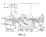
- FIG. 6 is a pull-down current attenuation circuit. It contains: four operational amplifiers, two inverters, two sets of (m + n) long channel PMOS transistors used as equivalent resistance, four MOS switches ( SW 5 to SW 8) and several MOS transistors.
- MOS transistor M 24 and operational amplifier opamp 5 constitute a first voltage follower.
- MOS transistor M 25 and operational amplifier opamp 6 constitute a second voltage follower.
- Source of MOS transistor M 24 (contact A) is connected to source of a set of n parallel PMOS transistors, and drain of MOS transistor M 24 is connected to one end of switch SW 5.
- Source of MOS transistor M 25 (contact B) is connected to drain of a set of m parallel PMOS transistors.
- Source of said m parallel PMOS transistors and drain of said n parallel PMOS transistors are connected to contact E.
- Grid of said m parallel PMOS transistors and grid of said n parallel PMOS transistors are connected to output of the inverter INV 2.
- MOS transistors M 30 and M 31 constitute a current mirror, input of the current mirror is connected to the input signal INsignal and output of the current mirror is connected with the MOS transistor M 28. Drain of the MOS transistor M 28 is connected with one end of switch SW 6 at contact E. Another end of switches SW 5 and SW 6 are all connected to input of the current mirror consisted of MOS transistors M 21 and M 22 at contact G.
- Output of the cascade transistor M 23, it grid is connected to bias voltage Vbias 1, is connected to output of the MOS transistor M 22.
- Input of the inverter INV 2 and control end of the switch SW 5 are connected to digital control signal INlogic , and output of the inverter INV 2 is connected to control end of the switch SW 6.
- MOS transistor M 26 and operational amplifier opamp 7 constitute a third voltage follower
- MOS transistor M27 and operational amplifier opamp 8 constitute a fourth voltage follower.
- Source (contact D) of the MOS transistor M 26 is connected to source of another set of n parallel PMOS transistors. Drain of the MOS transistor M26 is connected to power supply VDD.
- Source (contact C) of the MOS transistor M 27 is connected to drain electrode of another set of m parallel PMOS transistors.
- the SW 7 is connected between drain of the M 27 and contact G. Source of said m parallel PMOS transistors and drain of said n parallel PMOS transistors are connected to contact F.
- Grid of said m parallel PMOS transistors, and grid of said n parallel PMOS transistors, and control end of switch SW 8 are all connected to output of inverter INV 3.
- Input of current mirror consisted of MOS transistors M 32 and M 33, is connected to the common mode signal INcmfb , and output cascade transistor of the current mirror is MOS transistor M 29. Drain of the MOS transistor M 29 and one end of switch SW 8 are connected to contact F.
- Input of the inverter INV 3 and control end of the switch SW 7 are connected to the digital control signal INlogic .
- Input with phase coincidence of said four operational amplifiers are all connected to bias voltage Vbias 2, and grid of MOS transistors M 28 and M 29 is connected to bias voltage Vbias 3.
- VDD is a power supply.
- Vbias 1 and Vbias 3 are biases of CASCADE stage (a cascade, hereinafter, known as CASCADE), used to decrease channel length modulation effect of a MOS transistor.
- Vbias 2 is an externally added bias, used for DC bias of an equivalent resistance.
- INlogic is a digital control signal for controlling step attenuation
- INsignal is an input signal to be attenuated
- INcmfb is a CMFB current input
- Iout is a current output.
- I INsignal is current of the input signal
- I INcmfb is CMFB current (equals to the DC component of input signal current
- I AC is AC component of the input signal current.
- I out is an output current
- I(G) is an input current of the current mirror M 21 and M 22 at the contact G.
- control accuracy mainly depends on (1) match of m MOS transistors and n MOS transistors; (2) an offset voltage of operational amplifier (hereinafter, known as OFFSET).
- OFFSET of operational amplifier is related to integrated circuit manufacture technology, at present it is about 2mV.
- Match of MOS transistors can be solved by increasing MOS transistor area.
- deviation current during step control is a ratio of an operational amplifier OFFSET voltage and a MOS transistor conducting resistance used as equivalent resistance. Therefore, increasing channel length of MOS transistor can increase transistor conducting resistance to increase step control accuracy.
- maximum deviation current is 1uA; this means that when I INsignal is 100uA, step control accuracy is 1%.
- control accuracy relates to MOS transistors match accuracy; so for MOS transistors match when m or n has a smaller value, they can be increased with same proportion to utilize manufacture technology for raising step control accuracy.
- Corresponding relationship between number of said long channel PMOS transistors m , n, which are used for equivalent resistance, and DB attenuation value are as follow: when m takes 1 and n takes 9, DB attenuation value is -1; when m takes 2 and n takes 8, DB attenuation value is -2; when m takes 9 and n takes 16, DB attenuation value is -4; when m takes 6 and n takes 4, DB attenuation value is -8; and when m takes 21 and n takes 4, DB attenuation value is -16.
- FIG. 7 shows an injection current attenuation circuit, which contains four operational amplifiers, one inverter, two sets of ( m + n ) long channel NMOS transistors used as equivalent resistance, four MOS switches ( SW 1 to SW 4) and several MOS transistors.
- MOS transistor M 7 and operational amplifier opamp 1 constitute a first voltage follower
- MOS transistor M 8 and operational amplifier opamp 2 constitute a second voltage follower.
- Source and drain of MOS transistor M7 are connected to drains of a set of n parallel NMOS transistors and one end of switch SW 1, respectively.
- Source of MOS transistor M 8 is connected to sources of a set of m NMOS transistors, connected in parallel.
- Drains of said m NMOS transistors, sources of said n NMOS and switch SW 2 are connected to drain of MOS transistor M3.
- Input of current mirror consisted of MOS transistors M 1 and M2, is connected to input signal INsignal , and output of the current mirror is cascaded to MOS transistor M3.
- One end of switches SW 1, SW 2 and SW 3 is connected to input of current mirror, consisted of MOS transistors M 12 and M 13, and output of the current mirror is cascaded to MOS transistor M 11.
- Control ends of switches SW 1 and SW 3, said inverter INV 1 input, and grids of said m NMOS transistors and said n NMOS transistors are all connected to digital control signal INlogic.
- Output of inverter INV 1 is connected to control ends of switches SW 2 and SW 4.
- MOS transistor M 9 and operational amplifier opamp 3 constitute a third voltage follower
- MOS transistor M 10 and operational amplifier opamp 4 constitute a fourth voltage follower.
- Source of MOS transistor M 9 is connected to drains of another set of n parallel NMOS transistors, and drain of MOS transistor M 9 is connected to the ground.
- Source and drain of MOS transistor M 10 are connected to sources of another set of m parallel NMOS transistors and another end of switch SW 3, respectively. Grid of said m NMOS transistors and said n NMOS transistors are all connected to digital control signal INlogic.
- Input of current mirror consisted of MOS transistors M 4 and M 5, is connected to common mode signal INcmfb , and output of the current mirror is cascaded to MOS transistor M 6.
- Drain of MOS transistor M 6 drain of said m NMOS transistors and source of said n NMOS transistors are all connected to one end of switch SW 4, another end of switch SW 4 is connected to the ground.
- Phase coincidence input terminal of said four operational amplifiers are all connected to bias voltage Vbias 2
- grid of MOS transistors M 3 and M 6 are connected to bias voltage Vbias 1.
- an equivalent resistance implementation is also related to MOS transistor working state; in general, when MOS transistor equivalent resistance is working at a stable conducting state, the MOS transistor grid voltage VGS wants to be greater than 1.6V.
- Corresponding relationship between number of said long channel NMOS transistor m , n and DB attenuation value is as follow: when m takes 1 and n takes 9, DB attenuation value is -1; when m takes 2 and n takes 8, DB attenuation value is -2; when m takes 9 and n takes 16, DB attenuation value is -4; when m takes 6 and n takes 4, DB attenuation value is -8; and when m takes 21 and n takes 4, DB attenuation value is -16.
- INsignal is the signal current input
- INcmfb is the CMFB current input
- INlogic is the input of step attenuation digital control signal
- Vbias 1 and Vbias 3 are the bias voltage inputs of CASCADE stage
- Iout is the current output
- VDD is the power supply.
- MOS transistors in parallel, and n MOS transistors, in parallel, should be adjusted gently according to the necessary state; when their grid voltage is 3.3V and the drain voltage of MOS transistor M 3 is at 1.7 to 1.4V, they can work at equivalent resistance zone. When the drain voltage is too high, it is possible that equivalent resistance does not conduct enough; and when the drain voltage of M3 is too low, there is a higher requirement to operational amplifiers performance.
- Another current attenuation circuit implementation scheme of the invention is by using current sources match to attenuate.
- attenuation error of current source mainly comes from channel length modulation effect of devices, so in the design by appropriate increase device length and adjusting device working area, attenuation error will be decreased effectively.
- PMOS current attenuation circuit and NMOS current attenuation circuit are designed, respectively, in order to use different noise suppression ability of NMOS current source and PMOS current source. In principle, these two circuits are the same, only the polarity of signal attenuation is opposite.
- FIG. 8 shows a current attenuation circuit of P trap technology, which contains: MOS switches SW 11 and SW 12, an inverter INV 4, a MOS transistor M 41 and a current mirror I ; an area A1 consisted of ( m + n ) NMOS transistors connected in parallel, it grids and drains are connected together; an area B1 consisted of ( m + n ) NMOS transistors connected in parallel, it drains are connected to the source of MOS transistor M 41 across the MOS switch SW 11; an area C1 consisted of n NMOS transistors connected in parallel, it drains are connected with the output of current mirror I ; grid of areas A1, B1 and C1 are all connected to a input Iinsignal , source of areas A1, B1 and C1 are all connected to the ground GND; an area D1 consisted of ( m + n ) PMOS transistors connected in parallel, it grids and drains are mutually connected; an area E1 consisted of m PMOS transistors connected in parallel
- the circuit is divided into five areas A1, B1, C1, D1, and E1.
- Areas D1 and E1 constitute common mode feedback current attenuation stage
- areas A1 and B1 constitute signal current copy stage
- areas C1 and A1 constitute signal current attenuation stage.
- the area D1 is consisted of ( m + n ) PMOS transistors connected in parallel, with a common source, a common grid and a common drain.
- the area E1 is consisted of m PMOS transistors connected in parallel, with a common source, a common grid and a common drain.
- Areas A1 and B1 are consisted of ( m + n ) NMOS connected in parallel, with a common source, a common grid and a common drain.
- the area C1 is consisted of n NMOS transistors connected in parallel, with a common source, a common grid and a common drain.
- the Iincmfb is a common mode feedback current input
- the Iinsignal is a signal input
- the INlogic is a step gain digital control input
- the Vbias is bias voltage
- Iout is current output.
- the common mode feedback input Iincmfb is a DC current
- the signal input Iinsignal is DC current I DC plus AC current I AC .
- the DC component of common mode feedback input equals to the DC component of signal input, and the bias voltage Vbias decreases effectively the MOS transistor channel length modulate effect.
- Iinsignal I DC + I AC
- m is the number of PMOS transistors in area E1 ( m + n ) is the number of PMOS transistors in area D1. It can be seen from the formula above, common mode feedback current cut in current mirror is a proportional relationship with ratio of transistor number in areas D1 and E1.
- Attenuation of AC signal is n /( m + n ), and DC signal keeps unchanged.
- each stage attenuates AC signal and keeps DC component unchanged.
- the attenuation of AC signal is n /( m + n ), where n and m is a number of transistors.
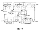
- FIG.9 shows a current attenuation circuit, with N trap technology, which contains: MOS switches SW 13 and SW 14, an inverter INV 5, a MOS transistor M 42 and current mirrors II and III.
- An area C2 that is consisted of ( m + n ) PMOS transistors connected in parallel, it grids and drains are connected together.
- An area D2 that is consisted of ( m + n ) PMOS transistors connected in parallel, it drains are connected to input of the current mirror II.
- E2 that is consisted of n PMOS transistors connected in parallel, it drains are connected to input of the current mirror III .
- Grids of areas C2, D2 and E2 are all connected to signal input Iinsignal, sources of areas C2, D2 and E2 are all connected to power supply VDD.
- Grids of areas A2 and B2 are all connected to common mode signal input Iincmfb , and sources of areas A2 and B2 are all connected to ground GND.
- the MOS switch SW 13 is connected between source of the MOS transistor M 42 and the current mirror II , and
- the MOS switch SW 14 is connected between source of the MOS transistor M 42 and drains of the area B2.
- the third end of MOS switches SW 13 and SW 14 is connected to power supply VDD, and the control end of MOS switch SW 14 and input of the inverter INV 5 are connected to digital control signal INlogic.
- the output of inverter INV 5 is connected to the control end of MOS switch SW 13; and the drain of MOS transistor M 42, it grid is connected to the bias voltage Vbias , is the current output Iout .
- step attenuation control circuit is divided into five areas: A2, B2, C2, D2 and E2.
- Areas A2 and B2 constitute common mode feedback current attenuation stage.
- Areas C2 and D2 constitute signal current copy stage.
- Areas c2 and E2 constitute signal current attenuation stage.
- the area A2 is consisted of ( m + n ) NMOS transistors, connected in parallel, with a common source, a common grid and a common drain.
- the area B2 is consisted of m NMOS transistors, connected in parallel, with a common source, a common grid and a common drain.
- Areas C2 and D2 are consisted of ( m + n ) PMOS transistors, connected in parallel, with a common source, a common grid and a common drain, respectively.
- the area E2 is consisted of n PMOS transistors, connected in parallel, with a common source, a common grid and a common drain.
- Iincmfb is a common mode feedback current input
- Iinsignal is a signal input
- INlogic is a step gain digital control signal input
- Vbias is a bias voltage
- Iout is a current output.
- output AC signal current is equal to input current, i.e. attenuation is 0DB.
- signal attenuation is n/(m+n).
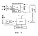
- FIG. 10 shows a typical application example of the invention.
- peripherals such as ADC and DAC etc., used as interface for DSP.
- ADC automatic gain control circuit
- DAC step attenuation circuit
- a step attenuation circuit is set after DAC to adjust output signal amplitude.
- AGC automatic gain control circuit
- a technology used to manufacture digital integrated circuit is generally used to integrate AGC and ADC circuit. Manufacturing technology of the step attenuation control circuit of the invention is compatible with typical digital integrated circuit manufacturing technology, so DSP and step attenuation control circuit can be integrated on one chip to decrease system cost and increase system reliability effectively.
- step attenuation control circuit can be used in fields such as ADSL, VDSL and video band transmission etc.
- an analog input signal is inputted from VinP and VinN, and CM is a common mode voltage input used to adjust circuit working point.
- CM is a common mode voltage input used to adjust circuit working point.
- the three input signal are converted from voltage to current.
- the current signals enter a current mode gain control stage to adjust gain, then the amplified signals are converted from current to voltage.
- the voltage signals are outputted to ADC by three lines to convert from analogy to digital, and the digital signal enters DSP to have necessary processing.
- DSP determines that ADC converting accuracy is unsatisfied, it uses BUS gain control b[0 - 4] to adjust amplification multiple of current mode gain stage until it is satisfied.
- DSP can output the processed signal such as image data to some peripheral digital equipment such PC etc., and DSP can also output another digital signal to DAC to convert to an analog output signal, such as stereo audio signal etc.
- the DAC output after filtering, is connected to an output stage to have a power output.
- DSP will attenuate the signal according to the channel characteristics, and then sends the attenuated signal to power amplifier.
- FIG. 5 shows relationship between digital control signal and attenuation, wherein sine waves are simplified.
- a digital input is 0, an output equals to the input, the attenuation is 0DB.
- a digital input signal is 31, an output sine wave corresponding to the input sine wave is 0.0282, i.e. -31DB.
- the signal attenuated is only the AC component, and the DC component is unchanged. Therefore, the purpose of only amplifying AC component without isolating capacitor is obtained. Consequently, circuits can be directly coupled with later stages.
- current mode DC suppression circuit has wider bandwidth, so in a wider frequency domain, DC component of a signal is effectively suppressed and the current mode CMRR has a stable value.
Landscapes
- Amplifiers (AREA)
- Networks Using Active Elements (AREA)
- Analogue/Digital Conversion (AREA)
- Control Of Eletrric Generators (AREA)
- Control Of Electric Motors In General (AREA)
- Air Bags (AREA)
- Oscillators With Electromechanical Resonators (AREA)
- Electrophonic Musical Instruments (AREA)
Abstract
Description


| DB attenuation | Real multiple | DB attenuation | Real multiple | DB attenuation | Real multiple | DB attenuation | Real multiple |
| 0 | 1.00E+00 | -8 | 3.98E-01 | -16 | 1.58E-01 | -24 | 6.31E-02 |
| -1 | 8.91E-01 | -9 | 3.55E-01 | -17 | 1.41E-01 | -25 | 5.62E-02 |
| -2 | 7.94E-01 | -10 | 3.16E-01 | -18 | 1.26E-01 | -26 | 5.07E-02 |
| -3 | 7.08E-01 | -11 | 2.82E-01 | -19 | 1.12E-01 | -27 | 4.47E-02 |
| -4 | 6.31E-01 | -12 | 2.51E-01 | -20 | 1.00E-01 | -28 | 3.98E-02 |
| -5 | 5.62E-01 | -13 | 2.24E-01 | -21 | 8.91E-02 | -29 | 3.55E-02 |
| -6 | 5.01E-01 | -14 | 2.00E-01 | -22 | 7.94E-02 | -30 | 3.16E-02 |
| -7 | 4.47E-01 | -15 | 1.78E-01 | -23 | 7.08E-02 | -31 | 2.82E-02 |
RO8N(P)=(1.0-0.891)*R1P(N)=0.109R1P(N).
RO7N(P) = (0.891-0.794)*R1P(N) = 0.097R1P(N).
| DB attenuation value | Real attenuation value | m value | n value |
| -1 | 8.91E-01 | 1 | 9 |
| -2 | 7.94E-01 | 2 | 8 |
| -4 | 6.31E-01 | 9 | 16 |
| -8 | 3.98E-01 | 6 | 4 |
| -16 | 1.58E-01 | 21 | 4 |
Claims (8)
- A current mode step attenuation control circuit with digital technology, it is characterized that the circuit comprises:several stages of current attenuation circuit, the current attenuation circuits are serially connected;a digital control input of each current attenuation circuit stage is connected with a digital control signal; a common mode feedback signal input of each current attenuation circuit stage is connected with a common mode feedback current; a bias input of each current attenuation circuit stage is connected with a bias voltage; andan analog input signal is connected to input of the first stage of current attenuation circuit.
- The circuit according to Claim 1, wherein the current mode step attenuation control circuit comprises 2 to 6 stages of current attenuation circuit.
- The circuit according to Claim 2, wherein the current mode step attenuation control circuit comprises 5 stages of current attenuation circuit.
- The circuit according to Claim 1, wherein the current attenuation circuit has at least terminals: a digital control input, a common mode feedback signal input, a bias input, an signal input, an signal output and a power supply.
- The circuit according to Claim 4, wherein the current attenuation circuit comprises four operational amplifiers opamp5 to opamp8, two inverters INV2 and INV3, two sets of m+n long channel PMOS transistors used as equivalent resistance, four MOS switches SW5 to SW8 and several MOS transistors;
the MOS transistor M24 and the operational amplifier opamp5 constituting a first voltage follower; the MOS transistor M25 and the operational amplifier opamp6 constituting a second voltage follower, source and drain of the MOS transistor M24 connecting to source of a set of n parallel PMOS transistors and one end of the switch SW5, respectively; source of the MOS transistor M25 connecting to drain of a set of m parallel PMOS transistors; sources of the m parallel PMOS transistors, drains of then n parallel PMOS transistors and drain of the MOS transistor M28 all connecting to one end of the switch SW6; grid of the m parallel PMOS transistors, grid of the n parallel PMOS transistors and control end of the switch SW6 all connecting to output of the inverter INV2; input and output of a first current mirror consisted of first pair of MOS transistors connecting to the signal input INsignal and cascading to the MOS transistor M28, respectively; input and output of a second current mirror consisted of second pair of MOS transistors connecting to another end of the switches SW5 and SW6 and cascading to the MOS transistor M23, respectively; input of the inverter INV2 and control end of the switch SW5 connecting to the digital control input INlogic;
the MOS transistor M26 and the operational amplifier opamp7 constituting a third voltage follower; the MOS transistor M27 and the operational amplifier opamp8 constituting a fourth voltage follower; source and drain of the MOS transistor M26 connecting to source of another set of n parallel PMOS transistors and the power supply VDD, respectively; source of the MOS transistor M27 connecting to drain of another set of m parallel PMOS transistors; the switch SW7 crossing between drain of the MOS transistor M27 and input of the second current mirror; source of the m parallel PMOS transistors, drain of the n parallel PMOS transistors and drain of the MOS transistor M29 all connecting to one end of the switch SW8 connected to the power supply VDD with another end; grid of the m parallel PMOS transistors, grid of the n parallel PMOS transistors and control end of the switch SW8 all connecting to output of the inverter INV3; input of a third current mirror consisted of third pair MOS transistors connecting to the common mode feedback signal input INcmfb, output of the third current mirror cascading to the MOS transistor M29; input of the inverter INV3 and control end of the switch SW7 connecting to the digital control input INlogic. - The circuit according to Claim 4, wherein the current attenuation circuit comprises four operational amplifiers opamp1 to opamp4, one inverter INV1, two sets of m+n long channel NMOS transistors used for equivalent resistance, four MOS switches SW1 to SW4 and several MOS transistors;
the MOS transistor M7 and the operational amplifier opamp1 constituting a first voltage follower; the MOS transistor M8 and the operational amplifier opamp2 constituting a second voltage follower; source and drain of the MOS transistor M7 connecting to drain of a set of n parallel NMOS transistors and one end of the switch SW1, respectively; source of the MOS transistor M8 connecting to source of a set of m parallel NMOS transistors; input and output of a first current mirror, consisted of first pair of MOS transistors, connecting to the signal input INsignal and cascading to the MOS transistor M3, respectively; drain of the m parallel NMOS transistors, source of n parallel NMOS transistors and the switch SW2 all connecting to drain of the MOS transistor M3; input and output of a second current mirror, consisted of second pair of MOS transistors, connecting to one end of switches SW1 to SW3 and cascading to the MOS transistor M11, respectively; control end of switches SW1 and SW3, input of the inverter INV1, gird of the m parallel NMOS transistors and the n parallel NMOS transistors all connecting to the digital control input INlogic; output of the inverter INV1 connecting to control end of switches SW2 and SW4;
the MOS transistor M9 and the operational amplifier opamp3 constituting a third voltage follower, and the MOS transistor M10 and the operational amplifier opamp4 constituting a fourth voltage follower; source and drain of the MOS transistor M9 connecting to drain of another set of n parallel NMOS transistors and the power supply ground, respectively; source and drain of the MOS transistor M10 connecting to source of another set of m parallel NMOS transistors and another end of the switch SW3, respectively; grid of the m parallel NMOS transistors and the n parallel NMOS transistors connecting to the digital control input INlogic; input and output of a third current mirror, consisted of third pair MOS transistors, connecting to the common mode feedback signal input INcmfb and cascading to the MOS transistor M6, respectively; drain of the m parallel NMOS transistors, source of the n parallel NMOS transistors and drain of the MOS transistor M6 all connecting to one end of the switch SW4; another end of the switch SW4 connecting to the power supply ground. - The circuit according to Claim 4, wherein the current attenuation circuit comprises:two MOS switches SW11 and SW12, one inverter INV4, one MOS transistor M41 and one current mirror I;one area A1 consisted of m+n parallel NMOS transistors, grid and drain of the area A1 connecting to each other;one area B1 consisted of m+n parallel NMOS transistors, the MOS switch SW11 crossing between drain of the area B1 and the MOS transistor M41;one area C1 consisted of n parallel NMOS transistors, drain of the area C1 connecting to output of the current mirror I, grid of the areas A1, B1 and C1 all connecting to the signal input Iinsignal, source of the A1, B1 and C1 all connecting to the power supply GND;one area D1 consisted of m+n parallel PMOS transistors, grid and drain of the area D1 connecting to each other;one area E1 consisted of m parallel PMOS transistors, drain of the area E1 connecting to input of the current mirror I; grid of the areas D1 and E1 all connecting to the common mode feedback signal input Iincmfb, source of the areas D1 and E1 all connecting to the power supply VDD;the MOS switch SW12 crossing between the MOS transistor M41 and drain of the C1 area; third end of MOS switches SW11 and SW12 all connecting to the power supply VDD; control end of the MOS switch SW12 and input of the inverter INV4 all connecting to the digital control input INlogic; output of the inverter INV4 connecting to control end of the MOS switch SW11; grid of the MOS transistor M41 connecting to the bias voltage and drain of the MOS transistor M41 being the signal output Iout.
- The circuit according to Claim 4, wherein the current attenuation circuit comprises:two MOS switches SW13 and SW14, one inverter INV5, one MOS transistor M42, two current mirrors II and III;one area C2 consisted of m+n parallel PMOS transistors, grid and drain of the area C2 connecting to each other;one area D2 consisted of m+n parallel PMOS transistors, drain of the area D2 connecting to input of the current mirror II;one area E2 consisted of n parallel PMOS transistors, drain of the area E2 connecting to input of the current mirror III; grid of the areas C2, D2 and E2 all connecting to the signal input Iinsignal, source of the areas C2, D2 and E2 all connecting to the power supply VDD;one area A2 consisted of m+n parallel NMOS transistors, grid and drain of the area A2 connecting to each other;one area B2 consisted of m parallel NMOS transistors, drain of the area B2 connecting to output of the current mirror III, grid of the areas A2 and B2 all connecting to the common mode feedback signal input Iincmfb, source of the areas A2 and B2 all connecting to the power supply GND;the MOS switch SW13 crossing between the MOS transistor M42 and the current mirror II; the MOS switch SW14 crossing between the MOS transistor M42 and drain of the area B2; third end of the MOS switches SW13 and SW14 all connecting to the power supply VDD; control end of the MOS switch SW14 and input of the inverter INV5 connecting to the digital control input INlogic; output of the inverter INV5 connecting to control end of the switch SW13; grid of the MOS transistor M42 connecting to the bias voltage and drain of the MOS transistor M42 being the signal output Iout.
Applications Claiming Priority (3)
| Application Number | Priority Date | Filing Date | Title |
|---|---|---|---|
| CNB00101594XA CN1142627C (en) | 2000-01-26 | 2000-01-26 | Current Mode Step Decay Control Circuit of Digital Technology |
| CN101594X | 2000-01-26 | ||
| PCT/CN2001/000097 WO2001056152A1 (en) | 2000-01-26 | 2001-01-22 | A digital technologic attenuate control circuit of current-model step by step |
Publications (3)
| Publication Number | Publication Date |
|---|---|
| EP1271777A1 true EP1271777A1 (en) | 2003-01-02 |
| EP1271777A4 EP1271777A4 (en) | 2006-12-20 |
| EP1271777B1 EP1271777B1 (en) | 2008-11-05 |
Family
ID=4576086
Family Applications (1)
| Application Number | Title | Priority Date | Filing Date |
|---|---|---|---|
| EP01905585A Expired - Lifetime EP1271777B1 (en) | 2000-01-26 | 2001-01-22 | A digital technologic attenuate control circuit of current-model step by step |
Country Status (7)
| Country | Link |
|---|---|
| US (1) | US6542018B1 (en) |
| EP (1) | EP1271777B1 (en) |
| CN (1) | CN1142627C (en) |
| AT (1) | ATE413727T1 (en) |
| AU (1) | AU2001233571A1 (en) |
| DE (1) | DE60136447D1 (en) |
| WO (1) | WO2001056152A1 (en) |
Families Citing this family (5)
| Publication number | Priority date | Publication date | Assignee | Title |
|---|---|---|---|---|
| JP4601615B2 (en) * | 2003-07-07 | 2010-12-22 | アナログデバイス,インコーポレイテッド | system |
| US8710899B2 (en) * | 2008-09-17 | 2014-04-29 | Lockheed Martin Corporation | Stepped delay control of integrated switches |
| CN102355615B (en) * | 2011-06-10 | 2014-03-12 | 无锡市晶源微电子有限公司 | Internal integration method for audio frequency deemphasis network |
| US9595937B2 (en) | 2014-09-17 | 2017-03-14 | Texas Instruments Incorporated | Programmable step attenuator with cross connection |
| CN115296620B (en) * | 2022-09-29 | 2022-12-30 | 深圳飞骧科技股份有限公司 | Multi-band adjustable gain low-noise amplifier |
Family Cites Families (10)
| Publication number | Priority date | Publication date | Assignee | Title |
|---|---|---|---|---|
| US5006735A (en) * | 1990-01-23 | 1991-04-09 | Triquint Semiconductor, Inc. | Method and apparatus for compensating a solid state attenuator |
| DE69306603T2 (en) | 1992-02-11 | 1997-06-05 | Philips Electronics Nv | Current divider and integrated circuit with multiple current dividers |
| EP0555905B1 (en) * | 1992-02-11 | 1996-12-18 | Koninklijke Philips Electronics N.V. | Current divider and integrated circuit comprising a plurality of current dividers |
| US5281928A (en) * | 1992-10-26 | 1994-01-25 | M/A-Com, Inc. | Electronic attenuator |
| US5623228A (en) * | 1993-05-17 | 1997-04-22 | Dan Inbar | Non-linear feedback network providing a linear transfer function |
| US5440280A (en) * | 1993-09-17 | 1995-08-08 | Mpr Teltech Ltd. | Digital microwave multi-bit attenuator |
| JP3362931B2 (en) * | 1993-09-30 | 2003-01-07 | ソニー株式会社 | Attenuator circuit |
| US5442352A (en) * | 1994-01-14 | 1995-08-15 | Motorola, Inc. | Linear attenuator for current-mode digital-to-analog converter (DAC) or the like |
| US6060933A (en) * | 1998-07-08 | 2000-05-09 | Analog Devices, Inc. | Electronic vernier systems and methods |
| US6229375B1 (en) * | 1999-08-18 | 2001-05-08 | Texas Instruments Incorporated | Programmable low noise CMOS differentially voltage controlled logarithmic attenuator and method |
-
2000
- 2000-01-26 CN CNB00101594XA patent/CN1142627C/en not_active Expired - Lifetime
-
2001
- 2001-01-22 WO PCT/CN2001/000097 patent/WO2001056152A1/en not_active Ceased
- 2001-01-22 AT AT01905585T patent/ATE413727T1/en not_active IP Right Cessation
- 2001-01-22 DE DE60136447T patent/DE60136447D1/en not_active Expired - Lifetime
- 2001-01-22 EP EP01905585A patent/EP1271777B1/en not_active Expired - Lifetime
- 2001-01-22 AU AU2001233571A patent/AU2001233571A1/en not_active Abandoned
-
2002
- 2002-07-26 US US10/206,560 patent/US6542018B1/en not_active Expired - Lifetime
Also Published As
| Publication number | Publication date |
|---|---|
| US6542018B1 (en) | 2003-04-01 |
| DE60136447D1 (en) | 2008-12-18 |
| CN1142627C (en) | 2004-03-17 |
| EP1271777A4 (en) | 2006-12-20 |
| AU2001233571A1 (en) | 2001-08-07 |
| EP1271777B1 (en) | 2008-11-05 |
| CN1307405A (en) | 2001-08-08 |
| WO2001056152A1 (en) | 2001-08-02 |
| ATE413727T1 (en) | 2008-11-15 |
Similar Documents
| Publication | Publication Date | Title |
|---|---|---|
| US7586373B2 (en) | Fully differential class AB amplifier and amplifying method using single-ended, two-stage amplifier | |
| US7088180B2 (en) | Programmable gain current amplifier | |
| KR100946815B1 (en) | Programmable Low Noise Amplifiers and Methods | |
| JPH0779121A (en) | Calculation transconductance amplifier of wide tuning range | |
| US5789981A (en) | High-gain operational transconductance amplifier offering improved bandwidth | |
| US6876256B2 (en) | Balanced amplifier and filter using the same | |
| US6316997B1 (en) | CMOS amplifiers with multiple gain setting control | |
| US6737919B2 (en) | Method and apparatus for calibrating a Gm cell utilizing a replica Gm cell | |
| CN114172467B (en) | A reconfigurable ultra-wideband high-precision variable gain amplifier core circuit | |
| US8169263B2 (en) | Differential gm-boosting circuit and applications | |
| US20020171486A1 (en) | High gain, high bandwidth, fully differential amplifier | |
| US20060001489A1 (en) | Highly linear variable gain amplifier | |
| US4947135A (en) | Single-ended chopper stabilized operational amplifier | |
| KR20030040185A (en) | Variable gain amplifier and filter circuit | |
| EP1271777B1 (en) | A digital technologic attenuate control circuit of current-model step by step | |
| Lee | Low-voltage op amp design and differential difference amplifier design using linear transconductor with resistor input | |
| JP3854218B2 (en) | Balanced amplifier and filter using the same | |
| JPS63313903A (en) | Amplifier circuit and optical communication system using it | |
| JPH0380608A (en) | Push-pull amplifier | |
| CN101416386A (en) | High-linearity variable gain amplifier | |
| CN111697936A (en) | Low-power-consumption complementary digital variable gain amplifier | |
| US20050146382A1 (en) | Differential amplifier with improved frequency characteristic | |
| US6819167B2 (en) | Filter circuit | |
| US20230361737A1 (en) | Circuit having an amplifier stage and a current mirror loop or stability network | |
| SU1676065A1 (en) | Operational amplifiers based on cmos transistors |
Legal Events
| Date | Code | Title | Description |
|---|---|---|---|
| PUAI | Public reference made under article 153(3) epc to a published international application that has entered the european phase |
Free format text: ORIGINAL CODE: 0009012 |
|
| 17P | Request for examination filed |
Effective date: 20020816 |
|
| AK | Designated contracting states |
Kind code of ref document: A1 Designated state(s): AT BE CH CY DE DK ES FI FR GB GR IE IT LI LU MC NL PT SE TR |
|
| AX | Request for extension of the european patent |
Free format text: AL;LT;LV;MK;RO;SI |
|
| A4 | Supplementary search report drawn up and despatched |
Effective date: 20061122 |
|
| 17Q | First examination report despatched |
Effective date: 20071127 |
|
| GRAP | Despatch of communication of intention to grant a patent |
Free format text: ORIGINAL CODE: EPIDOSNIGR1 |
|
| GRAS | Grant fee paid |
Free format text: ORIGINAL CODE: EPIDOSNIGR3 |
|
| GRAA | (expected) grant |
Free format text: ORIGINAL CODE: 0009210 |
|
| AK | Designated contracting states |
Kind code of ref document: B1 Designated state(s): AT BE CH CY DE DK ES FI FR GB GR IE IT LI LU MC NL PT SE TR |
|
| REG | Reference to a national code |
Ref country code: GB Ref legal event code: FG4D |
|
| REG | Reference to a national code |
Ref country code: CH Ref legal event code: EP |
|
| REG | Reference to a national code |
Ref country code: IE Ref legal event code: FG4D |
|
| REF | Corresponds to: |
Ref document number: 60136447 Country of ref document: DE Date of ref document: 20081218 Kind code of ref document: P |
|
| NLV1 | Nl: lapsed or annulled due to failure to fulfill the requirements of art. 29p and 29m of the patents act | ||
| PG25 | Lapsed in a contracting state [announced via postgrant information from national office to epo] |
Ref country code: AT Free format text: LAPSE BECAUSE OF FAILURE TO SUBMIT A TRANSLATION OF THE DESCRIPTION OR TO PAY THE FEE WITHIN THE PRESCRIBED TIME-LIMIT Effective date: 20081105 Ref country code: ES Free format text: LAPSE BECAUSE OF FAILURE TO SUBMIT A TRANSLATION OF THE DESCRIPTION OR TO PAY THE FEE WITHIN THE PRESCRIBED TIME-LIMIT Effective date: 20090216 |
|
| PG25 | Lapsed in a contracting state [announced via postgrant information from national office to epo] |
Ref country code: FI Free format text: LAPSE BECAUSE OF FAILURE TO SUBMIT A TRANSLATION OF THE DESCRIPTION OR TO PAY THE FEE WITHIN THE PRESCRIBED TIME-LIMIT Effective date: 20081105 Ref country code: NL Free format text: LAPSE BECAUSE OF FAILURE TO SUBMIT A TRANSLATION OF THE DESCRIPTION OR TO PAY THE FEE WITHIN THE PRESCRIBED TIME-LIMIT Effective date: 20081105 |
|
| PG25 | Lapsed in a contracting state [announced via postgrant information from national office to epo] |
Ref country code: BE Free format text: LAPSE BECAUSE OF FAILURE TO SUBMIT A TRANSLATION OF THE DESCRIPTION OR TO PAY THE FEE WITHIN THE PRESCRIBED TIME-LIMIT Effective date: 20081105 Ref country code: DK Free format text: LAPSE BECAUSE OF FAILURE TO SUBMIT A TRANSLATION OF THE DESCRIPTION OR TO PAY THE FEE WITHIN THE PRESCRIBED TIME-LIMIT Effective date: 20081105 |
|
| PG25 | Lapsed in a contracting state [announced via postgrant information from national office to epo] |
Ref country code: MC Free format text: LAPSE BECAUSE OF NON-PAYMENT OF DUE FEES Effective date: 20090131 Ref country code: PT Free format text: LAPSE BECAUSE OF FAILURE TO SUBMIT A TRANSLATION OF THE DESCRIPTION OR TO PAY THE FEE WITHIN THE PRESCRIBED TIME-LIMIT Effective date: 20090406 Ref country code: SE Free format text: LAPSE BECAUSE OF FAILURE TO SUBMIT A TRANSLATION OF THE DESCRIPTION OR TO PAY THE FEE WITHIN THE PRESCRIBED TIME-LIMIT Effective date: 20090205 |
|
| REG | Reference to a national code |
Ref country code: CH Ref legal event code: PL |
|
| PLBE | No opposition filed within time limit |
Free format text: ORIGINAL CODE: 0009261 |
|
| STAA | Information on the status of an ep patent application or granted ep patent |
Free format text: STATUS: NO OPPOSITION FILED WITHIN TIME LIMIT |
|
| 26N | No opposition filed |
Effective date: 20090806 |
|
| REG | Reference to a national code |
Ref country code: IE Ref legal event code: MM4A |
|
| PG25 | Lapsed in a contracting state [announced via postgrant information from national office to epo] |
Ref country code: LI Free format text: LAPSE BECAUSE OF NON-PAYMENT OF DUE FEES Effective date: 20090131 Ref country code: CH Free format text: LAPSE BECAUSE OF NON-PAYMENT OF DUE FEES Effective date: 20090131 |
|
| PG25 | Lapsed in a contracting state [announced via postgrant information from national office to epo] |
Ref country code: IE Free format text: LAPSE BECAUSE OF NON-PAYMENT OF DUE FEES Effective date: 20090122 |
|
| PG25 | Lapsed in a contracting state [announced via postgrant information from national office to epo] |
Ref country code: GR Free format text: LAPSE BECAUSE OF FAILURE TO SUBMIT A TRANSLATION OF THE DESCRIPTION OR TO PAY THE FEE WITHIN THE PRESCRIBED TIME-LIMIT Effective date: 20090206 |
|
| PG25 | Lapsed in a contracting state [announced via postgrant information from national office to epo] |
Ref country code: IT Free format text: LAPSE BECAUSE OF FAILURE TO SUBMIT A TRANSLATION OF THE DESCRIPTION OR TO PAY THE FEE WITHIN THE PRESCRIBED TIME-LIMIT Effective date: 20081105 |
|
| PG25 | Lapsed in a contracting state [announced via postgrant information from national office to epo] |
Ref country code: LU Free format text: LAPSE BECAUSE OF NON-PAYMENT OF DUE FEES Effective date: 20090122 |
|
| PG25 | Lapsed in a contracting state [announced via postgrant information from national office to epo] |
Ref country code: TR Free format text: LAPSE BECAUSE OF FAILURE TO SUBMIT A TRANSLATION OF THE DESCRIPTION OR TO PAY THE FEE WITHIN THE PRESCRIBED TIME-LIMIT Effective date: 20081105 |
|
| PG25 | Lapsed in a contracting state [announced via postgrant information from national office to epo] |
Ref country code: CY Free format text: LAPSE BECAUSE OF FAILURE TO SUBMIT A TRANSLATION OF THE DESCRIPTION OR TO PAY THE FEE WITHIN THE PRESCRIBED TIME-LIMIT Effective date: 20081105 |
|
| REG | Reference to a national code |
Ref country code: FR Ref legal event code: PLFP Year of fee payment: 16 |
|
| REG | Reference to a national code |
Ref country code: FR Ref legal event code: PLFP Year of fee payment: 17 |
|
| REG | Reference to a national code |
Ref country code: FR Ref legal event code: PLFP Year of fee payment: 18 |
|
| PGFP | Annual fee paid to national office [announced via postgrant information from national office to epo] |
Ref country code: FR Payment date: 20191216 Year of fee payment: 20 |
|
| PGFP | Annual fee paid to national office [announced via postgrant information from national office to epo] |
Ref country code: DE Payment date: 20200107 Year of fee payment: 20 Ref country code: GB Payment date: 20200115 Year of fee payment: 20 |
|
| REG | Reference to a national code |
Ref country code: DE Ref legal event code: R071 Ref document number: 60136447 Country of ref document: DE |
|
| REG | Reference to a national code |
Ref country code: GB Ref legal event code: PE20 Expiry date: 20210121 |
|
| PG25 | Lapsed in a contracting state [announced via postgrant information from national office to epo] |
Ref country code: GB Free format text: LAPSE BECAUSE OF EXPIRATION OF PROTECTION Effective date: 20210121 |