EP1271743A2 - Schaltungstopologie für einen bidirektionalen Energietransfer - Google Patents
Schaltungstopologie für einen bidirektionalen Energietransfer Download PDFInfo
- Publication number
- EP1271743A2 EP1271743A2 EP02012846A EP02012846A EP1271743A2 EP 1271743 A2 EP1271743 A2 EP 1271743A2 EP 02012846 A EP02012846 A EP 02012846A EP 02012846 A EP02012846 A EP 02012846A EP 1271743 A2 EP1271743 A2 EP 1271743A2
- Authority
- EP
- European Patent Office
- Prior art keywords
- mosfet
- circuit topology
- energy transfer
- connections
- gate
- Prior art date
- Legal status (The legal status is an assumption and is not a legal conclusion. Google has not performed a legal analysis and makes no representation as to the accuracy of the status listed.)
- Withdrawn
Links
Images
Classifications
-
- H—ELECTRICITY
- H03—ELECTRONIC CIRCUITRY
- H03K—PULSE TECHNIQUE
- H03K17/00—Electronic switching or gating, i.e. not by contact-making and –breaking
- H03K17/51—Electronic switching or gating, i.e. not by contact-making and –breaking characterised by the components used
- H03K17/56—Electronic switching or gating, i.e. not by contact-making and –breaking characterised by the components used by the use, as active elements, of semiconductor devices
- H03K17/687—Electronic switching or gating, i.e. not by contact-making and –breaking characterised by the components used by the use, as active elements, of semiconductor devices the devices being field-effect transistors
- H03K17/6871—Electronic switching or gating, i.e. not by contact-making and –breaking characterised by the components used by the use, as active elements, of semiconductor devices the devices being field-effect transistors the output circuit comprising more than one controlled field-effect transistor
- H03K17/6874—Electronic switching or gating, i.e. not by contact-making and –breaking characterised by the components used by the use, as active elements, of semiconductor devices the devices being field-effect transistors the output circuit comprising more than one controlled field-effect transistor in a symmetrical configuration
Definitions
- the present invention relates to a circuit topology for bidirectional energy transfer.
- Circuit topology is known from DE 195 48 612 A1.
- Circuit topologies for bidirectional, unregulated energy transfer known.
- the previous Realizations each see a circuit block for each transfer direction, which is a double execution of the circuit block means.
- the one for each circuit block each backward direction must usually protected against reverse polarity by a protective mechanism become.
- the object of the present invention is now a Circuit topology for bidirectional energy transfer to provide through which the bidirectional energy transfer is adjustable, which has as few components as possible and is easy and economical to implement.
- a circuit topology is provided for a bidirectional Energy transfer, with two channels each one Have MOSFET, wherein the circuit topology is characterized is that the MOSFET with their respective gate and Source connections are connected, and the control voltage is created through a common resistance.
- each a P-channel transistor with a voltage Uds ⁇ 0 im Forward operation the other with a voltage Uds> 0 is in reverse operation.
- the circuit topology according to the invention draws is preferably further characterized in that a switch is provided for selection of the current flow direction.
- the current flows from one Voltage U1 to the other voltage U2, in the other switch position vice versa accordingly.
- the actual value of the respective output voltage with a Setpoint value of a reference voltage Uref compared.
- the circuit topology is preferably also characterized by this from that an error amplifier is provided which is used for Generates a corresponding control signal, independently from the position of the switch.
- circuit topology can also be and capacitor elements for compensation of the control loop be supplemented.
- the circuit according to the invention makes it possible to use a bidirectional energy transfer via a 2 MOSFET To provide an actuator which is not only switching, but can also be operated analog.
- the advantage of the invention is, among other things, that the number of components and required control signals compared to the known circuit topologies for the bidirectional energy transfer roughly halved, which is a place economical and cost-effective implementation in an overall system facilitated.
- the invention can be used in battery-operated devices that have a contact socket for charging.
- the same can now also be used to supply the socket used by consumers, e.g. a mobile phone with charging socket via which also attachable accessories are supplied can be.
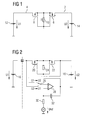
- FIG. 1 shows the schematic representation of a circuit topology for bidirectional energy transfer.
- Two feed lines 2, 4 are provided, each one Have MOSFET 6, 8. 1 can be seen the MOSFET 6, 8 connected to their gate and source connections.
- the control voltage is via a two MOSFET 6, 8 common resistor 10 applied.
- FIG. 2 is a schematic representation of the use the circuit topology for bidirectional energy transfer shown in a mobile phone.
- the area to the right of the dashed line denotes a mobile phone arrangement with a voltage source 16, at which in the illustrated embodiment is a battery or an accumulator.
- a own voltage source 18 generally a separate, pluggable Accessories what as an energy source or consumer serves, e.g. a charger or an MP3 player.
- the circuit in accordance with FIG. 2 has two P-channel MOSFETs 20 and 22 on.
- the gate and source connections of the MOSFET 20 are with the corresponding gate and source connections of the MOSFET 22 connected so that the control voltage via a two MOSFET 20, 22 common resistor 24 can be created.
- This configuration (common source) has bidirectional compared to the usual interconnection Switch (common drain) has the advantage that only one Control signal for both transistors 20, 22 is required. What is common to both configurations, however, is that each is always a P-channel transistor 20 with a drain-source voltage Uds ⁇ 0 is in forward operation, the other one Transistor 22 with a drain-source voltage Uds> 0 in reverse operation.
- An error amplifier 28 is also provided, which is independent the corresponding position of the switch 26 Control signal generated.
- the power supply of the error amplifier 28 is not shown in FIG. 2.
- Fig. 2 another resistance element 30 and a capacitor element 32 intended.
- the elements 30 and 32 are used for compensation of the control loop and are particularly suitable for analog operation the arrangement required.
- the circuit as shown in Fig. 2 serves a bidirectional Energy transfer via a single actuator enable which is not only switching, but also analog can be operated.
- a single actuator enable which is not only switching, but also analog can be operated.
Landscapes
- Direct Current Feeding And Distribution (AREA)
- Charge And Discharge Circuits For Batteries Or The Like (AREA)
- Networks Using Active Elements (AREA)
- Continuous-Control Power Sources That Use Transistors (AREA)
Abstract
Description
- Fig. 1
- die schematische Darstellung einer SchaltungsTopologie für einen bidirektionalen Energietransfer,
- Fig. 2
- die schematische Darstellung der Verwendung der Schaltungstopologie für einen bidirektionalen Energietransfer in einem Mobiltelefon.
Claims (3)
- Schaltungstopologie für einen bidirektionalen Energietransfer, mit zwei Zuleitungen (2, 4), die jeweils einen MOSFET (6, 8, 20, 22) aufweisen, wobei die MOSFET (6, 8, 20, 22) mit ihren Gate- und ihren Source-Anschlüssen verbunden sind und ein Widerstand (10, 24) zwischen die verbundenen Gate-Anschlüsse und die verbundenen Source-Anschlüsse der MOSFET geschaltet sind, und wobei ein Fehlerverstärker (28) zur Erzeugung einer Steuerspannung für die Gate-Anschlüsse der MOSFET vorgesehen ist und
der Fehlerverstärker (28) zum Vergleich eines Istwertes einer jeweiligen Ausgangsspannung (U1, U2) der Schaltungstopologie mit einem Sollwert einer Referenzspannung (Uref) angeordnet ist. - Schaltungstopologie nach Anspruch 1,
dadurch gekennzeichnet, dass ein Schalter (26) zur Auswahl der Stromflussrichtung vorgesehen ist. - Schaltungstopologie nach einem der Ansprüche 1 bis 2,
dadurch gekennzeichnet, dass sie in ein mobiles Telekommunikationsgerät integriert ist.
Applications Claiming Priority (2)
| Application Number | Priority Date | Filing Date | Title |
|---|---|---|---|
| DE10129353 | 2001-06-19 | ||
| DE2001129353 DE10129353C1 (de) | 2001-06-19 | 2001-06-19 | Schaltungstopologie für einen bidirektionalen Energietransfer |
Publications (2)
| Publication Number | Publication Date |
|---|---|
| EP1271743A2 true EP1271743A2 (de) | 2003-01-02 |
| EP1271743A3 EP1271743A3 (de) | 2005-01-05 |
Family
ID=7688572
Family Applications (1)
| Application Number | Title | Priority Date | Filing Date |
|---|---|---|---|
| EP02012846A Withdrawn EP1271743A3 (de) | 2001-06-19 | 2002-06-10 | Schaltungstopologie für einen bidirektionalen Energietransfer |
Country Status (2)
| Country | Link |
|---|---|
| EP (1) | EP1271743A3 (de) |
| DE (1) | DE10129353C1 (de) |
Cited By (2)
| Publication number | Priority date | Publication date | Assignee | Title |
|---|---|---|---|---|
| EP1482641A3 (de) * | 2003-05-20 | 2006-01-04 | AMI Semiconductor, Inc. | Vielfachfehlergeschützter spannungsseitiger Schalter mit Stromerfassung |
| EP4697602A1 (de) | 2024-08-14 | 2026-02-18 | Siemens Aktiengesellschaft | Common-source-konfiguration von zwei transistoren |
Families Citing this family (1)
| Publication number | Priority date | Publication date | Assignee | Title |
|---|---|---|---|---|
| JP4618164B2 (ja) * | 2005-09-20 | 2011-01-26 | 株式会社デンソー | スイッチ回路 |
Citations (2)
| Publication number | Priority date | Publication date | Assignee | Title |
|---|---|---|---|---|
| DE19548612A1 (de) | 1995-12-23 | 1997-06-26 | Bosch Gmbh Robert | Elektronischer Schalter |
| US5847912A (en) | 1996-05-03 | 1998-12-08 | Nat Semiconductor Corp | Active rectification and battery protection circuit |
Family Cites Families (3)
| Publication number | Priority date | Publication date | Assignee | Title |
|---|---|---|---|---|
| JPS63227215A (ja) * | 1987-03-17 | 1988-09-21 | Toshiba Corp | 半導体スイツチ回路 |
| US5287024A (en) * | 1993-01-21 | 1994-02-15 | Northern Telecom Limited | FET bidirectional switching arrangements and methods for preventing pn junctions of FETs from being forward-biased |
| US5635821A (en) * | 1995-06-30 | 1997-06-03 | National Semiconductor Corporation | Low cell charge enable circuit |
-
2001
- 2001-06-19 DE DE2001129353 patent/DE10129353C1/de not_active Expired - Lifetime
-
2002
- 2002-06-10 EP EP02012846A patent/EP1271743A3/de not_active Withdrawn
Patent Citations (2)
| Publication number | Priority date | Publication date | Assignee | Title |
|---|---|---|---|---|
| DE19548612A1 (de) | 1995-12-23 | 1997-06-26 | Bosch Gmbh Robert | Elektronischer Schalter |
| US5847912A (en) | 1996-05-03 | 1998-12-08 | Nat Semiconductor Corp | Active rectification and battery protection circuit |
Cited By (2)
| Publication number | Priority date | Publication date | Assignee | Title |
|---|---|---|---|---|
| EP1482641A3 (de) * | 2003-05-20 | 2006-01-04 | AMI Semiconductor, Inc. | Vielfachfehlergeschützter spannungsseitiger Schalter mit Stromerfassung |
| EP4697602A1 (de) | 2024-08-14 | 2026-02-18 | Siemens Aktiengesellschaft | Common-source-konfiguration von zwei transistoren |
Also Published As
| Publication number | Publication date |
|---|---|
| DE10129353C1 (de) | 2002-10-10 |
| EP1271743A3 (de) | 2005-01-05 |
Similar Documents
| Publication | Publication Date | Title |
|---|---|---|
| DE68917226T2 (de) | Gegen die Polaritätsumkehr seiner Versorgungsbatterie geschützte elektronische Schaltung. | |
| DE69530131T2 (de) | Schutzanordnung für eine aktive Fernsprechsleitungsschnittstellenschaltung | |
| DE19706946A1 (de) | Battierüberwachungseinheit | |
| DE2953275C2 (de) | ||
| DE60027899T2 (de) | System und verfahren zur unabhängigen versorgungsfolge integrierter schaltungen | |
| DE19548612A1 (de) | Elektronischer Schalter | |
| DE102009052212A1 (de) | System und Verfahren zum Schutz vor Batterieverlust in Geräten mit Verpolungsschutz | |
| DE102013203929A1 (de) | Verfahren zur ansteuerung eines halbleiterbauelements | |
| DE2710049C2 (de) | Ultraschall-Zahnbehandlungsgerät | |
| DE10129353C1 (de) | Schaltungstopologie für einen bidirektionalen Energietransfer | |
| DE3029814A1 (de) | Automatische spannungsversorgungs- schalteinrichtung | |
| DE69635483T2 (de) | Schaltkreis mit verriegelungseinrichtung | |
| EP1203933A1 (de) | Sensoranordnung zur Erfassung wenigstens eines Messwerts | |
| DE3622713A1 (de) | Schaltungsanordnung mit einer brueckenendstufe | |
| WO2017097497A1 (de) | High-side-schalter für die stromversorgung mindestens eines sensors | |
| DE19805491C1 (de) | Diodenschaltung mit idealer Diodenkennlinie | |
| DE3834867C1 (en) | Circuit arrangement for the parallel connection of power supply devices | |
| EP0696849A2 (de) | Steuergerät mit einer Schaltungsanordnung zum Schutz des Steuergerätes bei Unterbrechung der Steuergerätemasse | |
| WO2000011788A2 (de) | Treiberschaltung | |
| DE102021206080A1 (de) | Integrierte Schaltung und Verfahren zum Begrenzen eines schaltbaren Laststroms | |
| DE2921712A1 (de) | Vorrichtung zur fernsteuerung der winkelposition einer drehantenne | |
| DE69933319T2 (de) | Strombegrenzungsempfänger mit Impedanz- /Lastanpassung für einen Empfängerchip in abgeschaltetem Zustand | |
| DE102006004267A1 (de) | Bordnetz für ein Fahrzeug | |
| DE10226082B4 (de) | Schaltungsanordnung zur Strombegrenzung | |
| DE69922495T2 (de) | Schaltung zur Verbindung zwischen einem Autoradio und einer Kraftfahrzeugbatterie |
Legal Events
| Date | Code | Title | Description |
|---|---|---|---|
| PUAI | Public reference made under article 153(3) epc to a published international application that has entered the european phase |
Free format text: ORIGINAL CODE: 0009012 |
|
| AK | Designated contracting states |
Kind code of ref document: A2 Designated state(s): AT BE CH CY DE DK ES FI FR GB GR IE IT LI LU MC NL PT SE TR |
|
| AX | Request for extension of the european patent |
Free format text: AL;LT;LV;MK;RO;SI |
|
| PUAL | Search report despatched |
Free format text: ORIGINAL CODE: 0009013 |
|
| AK | Designated contracting states |
Kind code of ref document: A3 Designated state(s): AT BE CH CY DE DK ES FI FR GB GR IE IT LI LU MC NL PT SE TR |
|
| AX | Request for extension of the european patent |
Extension state: AL LT LV MK RO SI |
|
| RIC1 | Information provided on ipc code assigned before grant |
Ipc: 7H 03K 17/687 B Ipc: 7H 02M 3/158 B Ipc: 7H 02J 7/00 A |
|
| 17P | Request for examination filed |
Effective date: 20050606 |
|
| AKX | Designation fees paid |
Designated state(s): DE FR GB |
|
| RAP1 | Party data changed (applicant data changed or rights of an application transferred) |
Owner name: BENQ MOBILE GMBH & CO. OHG |
|
| 19U | Interruption of proceedings before grant |
Effective date: 20070101 |
|
| 19W | Proceedings resumed before grant after interruption of proceedings |
Effective date: 20070702 |
|
| 19W | Proceedings resumed before grant after interruption of proceedings |
Effective date: 20090803 |
|
| RAP1 | Party data changed (applicant data changed or rights of an application transferred) |
Owner name: PALM, INC. |
|
| 17Q | First examination report despatched |
Effective date: 20090824 |
|
| RAP1 | Party data changed (applicant data changed or rights of an application transferred) |
Owner name: HEWLETT-PACKARD DEVELOPMENT COMPANY, L.P. |
|
| RAP1 | Party data changed (applicant data changed or rights of an application transferred) |
Owner name: QUALCOMM INCORPORATED |
|
| STAA | Information on the status of an ep patent application or granted ep patent |
Free format text: STATUS: THE APPLICATION IS DEEMED TO BE WITHDRAWN |
|
| 18D | Application deemed to be withdrawn |
Effective date: 20150806 |