EP1271653A1 - Insulated-gate bipolar transistor, semiconductor device, method of manufacturing insulated-gate bipolar transistor, and method of manufacturing semiconductor device - Google Patents
Insulated-gate bipolar transistor, semiconductor device, method of manufacturing insulated-gate bipolar transistor, and method of manufacturing semiconductor device Download PDFInfo
- Publication number
- EP1271653A1 EP1271653A1 EP01273674A EP01273674A EP1271653A1 EP 1271653 A1 EP1271653 A1 EP 1271653A1 EP 01273674 A EP01273674 A EP 01273674A EP 01273674 A EP01273674 A EP 01273674A EP 1271653 A1 EP1271653 A1 EP 1271653A1
- Authority
- EP
- European Patent Office
- Prior art keywords
- layer
- collector
- bipolar transistor
- gate bipolar
- insulated gate
- Prior art date
- Legal status (The legal status is an assumption and is not a legal conclusion. Google has not performed a legal analysis and makes no representation as to the accuracy of the status listed.)
- Granted
Links
Images








Classifications
-
- H—ELECTRICITY
- H10—SEMICONDUCTOR DEVICES; ELECTRIC SOLID-STATE DEVICES NOT OTHERWISE PROVIDED FOR
- H10D—INORGANIC ELECTRIC SEMICONDUCTOR DEVICES
- H10D12/00—Bipolar devices controlled by the field effect, e.g. insulated-gate bipolar transistors [IGBT]
- H10D12/01—Manufacture or treatment
- H10D12/031—Manufacture or treatment of IGBTs
- H10D12/032—Manufacture or treatment of IGBTs of vertical IGBTs
-
- H—ELECTRICITY
- H10—SEMICONDUCTOR DEVICES; ELECTRIC SOLID-STATE DEVICES NOT OTHERWISE PROVIDED FOR
- H10P—GENERIC PROCESSES OR APPARATUS FOR THE MANUFACTURE OR TREATMENT OF DEVICES COVERED BY CLASS H10
- H10P10/00—Bonding of wafers, substrates or parts of devices
-
- H—ELECTRICITY
- H02—GENERATION; CONVERSION OR DISTRIBUTION OF ELECTRIC POWER
- H02M—APPARATUS FOR CONVERSION BETWEEN AC AND AC, BETWEEN AC AND DC, OR BETWEEN DC AND DC, AND FOR USE WITH MAINS OR SIMILAR POWER SUPPLY SYSTEMS; CONVERSION OF DC OR AC INPUT POWER INTO SURGE OUTPUT POWER; CONTROL OR REGULATION THEREOF
- H02M7/00—Conversion of AC power input into DC power output; Conversion of DC power input into AC power output
- H02M7/003—Constructional details, e.g. physical layout, assembly, wiring or busbar connections
-
- H—ELECTRICITY
- H10—SEMICONDUCTOR DEVICES; ELECTRIC SOLID-STATE DEVICES NOT OTHERWISE PROVIDED FOR
- H10D—INORGANIC ELECTRIC SEMICONDUCTOR DEVICES
- H10D12/00—Bipolar devices controlled by the field effect, e.g. insulated-gate bipolar transistors [IGBT]
- H10D12/01—Manufacture or treatment
- H10D12/031—Manufacture or treatment of IGBTs
- H10D12/032—Manufacture or treatment of IGBTs of vertical IGBTs
- H10D12/038—Manufacture or treatment of IGBTs of vertical IGBTs having a recessed gate, e.g. trench-gate IGBTs
-
- H—ELECTRICITY
- H10—SEMICONDUCTOR DEVICES; ELECTRIC SOLID-STATE DEVICES NOT OTHERWISE PROVIDED FOR
- H10D—INORGANIC ELECTRIC SEMICONDUCTOR DEVICES
- H10D12/00—Bipolar devices controlled by the field effect, e.g. insulated-gate bipolar transistors [IGBT]
- H10D12/411—Insulated-gate bipolar transistors [IGBT]
- H10D12/441—Vertical IGBTs
-
- H—ELECTRICITY
- H10—SEMICONDUCTOR DEVICES; ELECTRIC SOLID-STATE DEVICES NOT OTHERWISE PROVIDED FOR
- H10D—INORGANIC ELECTRIC SEMICONDUCTOR DEVICES
- H10D12/00—Bipolar devices controlled by the field effect, e.g. insulated-gate bipolar transistors [IGBT]
- H10D12/411—Insulated-gate bipolar transistors [IGBT]
- H10D12/441—Vertical IGBTs
- H10D12/461—Vertical IGBTs having non-planar surfaces, e.g. having trenches, recesses or pillars in the surfaces of the emitter, base or collector regions
- H10D12/481—Vertical IGBTs having non-planar surfaces, e.g. having trenches, recesses or pillars in the surfaces of the emitter, base or collector regions having gate structures on slanted surfaces, on vertical surfaces, or in grooves, e.g. trench gate IGBTs
-
- H—ELECTRICITY
- H10—SEMICONDUCTOR DEVICES; ELECTRIC SOLID-STATE DEVICES NOT OTHERWISE PROVIDED FOR
- H10D—INORGANIC ELECTRIC SEMICONDUCTOR DEVICES
- H10D62/00—Semiconductor bodies, or regions thereof, of devices having potential barriers
- H10D62/10—Shapes, relative sizes or dispositions of the regions of the semiconductor bodies; Shapes of the semiconductor bodies
- H10D62/13—Semiconductor regions connected to electrodes carrying current to be rectified, amplified or switched, e.g. source or drain regions
- H10D62/141—Anode or cathode regions of thyristors; Collector or emitter regions of gated bipolar-mode devices, e.g. of IGBTs
- H10D62/142—Anode regions of thyristors or collector regions of gated bipolar-mode devices
-
- H—ELECTRICITY
- H10—SEMICONDUCTOR DEVICES; ELECTRIC SOLID-STATE DEVICES NOT OTHERWISE PROVIDED FOR
- H10W—GENERIC PACKAGES, INTERCONNECTIONS, CONNECTORS OR OTHER CONSTRUCTIONAL DETAILS OF DEVICES COVERED BY CLASS H10
- H10W90/00—Package configurations
-
- H—ELECTRICITY
- H10—SEMICONDUCTOR DEVICES; ELECTRIC SOLID-STATE DEVICES NOT OTHERWISE PROVIDED FOR
- H10W—GENERIC PACKAGES, INTERCONNECTIONS, CONNECTORS OR OTHER CONSTRUCTIONAL DETAILS OF DEVICES COVERED BY CLASS H10
- H10W72/00—Interconnections or connectors in packages
- H10W72/071—Connecting or disconnecting
- H10W72/075—Connecting or disconnecting of bond wires
- H10W72/07551—Connecting or disconnecting of bond wires characterised by changes in properties of the bond wires during the connecting
- H10W72/07554—Connecting or disconnecting of bond wires characterised by changes in properties of the bond wires during the connecting changes in dispositions
-
- H—ELECTRICITY
- H10—SEMICONDUCTOR DEVICES; ELECTRIC SOLID-STATE DEVICES NOT OTHERWISE PROVIDED FOR
- H10W—GENERIC PACKAGES, INTERCONNECTIONS, CONNECTORS OR OTHER CONSTRUCTIONAL DETAILS OF DEVICES COVERED BY CLASS H10
- H10W72/00—Interconnections or connectors in packages
- H10W72/50—Bond wires
- H10W72/541—Dispositions of bond wires
- H10W72/547—Dispositions of multiple bond wires
-
- H—ELECTRICITY
- H10—SEMICONDUCTOR DEVICES; ELECTRIC SOLID-STATE DEVICES NOT OTHERWISE PROVIDED FOR
- H10W—GENERIC PACKAGES, INTERCONNECTIONS, CONNECTORS OR OTHER CONSTRUCTIONAL DETAILS OF DEVICES COVERED BY CLASS H10
- H10W72/00—Interconnections or connectors in packages
- H10W72/50—Bond wires
- H10W72/541—Dispositions of bond wires
- H10W72/547—Dispositions of multiple bond wires
- H10W72/5475—Dispositions of multiple bond wires multiple bond wires connected to common bond pads at both ends of the wires
-
- H—ELECTRICITY
- H10—SEMICONDUCTOR DEVICES; ELECTRIC SOLID-STATE DEVICES NOT OTHERWISE PROVIDED FOR
- H10W—GENERIC PACKAGES, INTERCONNECTIONS, CONNECTORS OR OTHER CONSTRUCTIONAL DETAILS OF DEVICES COVERED BY CLASS H10
- H10W72/00—Interconnections or connectors in packages
- H10W72/50—Bond wires
- H10W72/551—Materials of bond wires
- H10W72/552—Materials of bond wires comprising metals or metalloids, e.g. silver
- H10W72/5524—Materials of bond wires comprising metals or metalloids, e.g. silver comprising aluminium [Al]
-
- H—ELECTRICITY
- H10—SEMICONDUCTOR DEVICES; ELECTRIC SOLID-STATE DEVICES NOT OTHERWISE PROVIDED FOR
- H10W—GENERIC PACKAGES, INTERCONNECTIONS, CONNECTORS OR OTHER CONSTRUCTIONAL DETAILS OF DEVICES COVERED BY CLASS H10
- H10W72/00—Interconnections or connectors in packages
- H10W72/851—Dispositions of multiple connectors or interconnections
- H10W72/874—On different surfaces
- H10W72/884—Die-attach connectors and bond wires
-
- H—ELECTRICITY
- H10—SEMICONDUCTOR DEVICES; ELECTRIC SOLID-STATE DEVICES NOT OTHERWISE PROVIDED FOR
- H10W—GENERIC PACKAGES, INTERCONNECTIONS, CONNECTORS OR OTHER CONSTRUCTIONAL DETAILS OF DEVICES COVERED BY CLASS H10
- H10W74/00—Encapsulations, e.g. protective coatings
-
- H—ELECTRICITY
- H10—SEMICONDUCTOR DEVICES; ELECTRIC SOLID-STATE DEVICES NOT OTHERWISE PROVIDED FOR
- H10W—GENERIC PACKAGES, INTERCONNECTIONS, CONNECTORS OR OTHER CONSTRUCTIONAL DETAILS OF DEVICES COVERED BY CLASS H10
- H10W90/00—Package configurations
- H10W90/701—Package configurations characterised by the relative positions of pads or connectors relative to package parts
- H10W90/751—Package configurations characterised by the relative positions of pads or connectors relative to package parts of bond wires
- H10W90/753—Package configurations characterised by the relative positions of pads or connectors relative to package parts of bond wires between laterally-adjacent chips
-
- H—ELECTRICITY
- H10—SEMICONDUCTOR DEVICES; ELECTRIC SOLID-STATE DEVICES NOT OTHERWISE PROVIDED FOR
- H10W—GENERIC PACKAGES, INTERCONNECTIONS, CONNECTORS OR OTHER CONSTRUCTIONAL DETAILS OF DEVICES COVERED BY CLASS H10
- H10W90/00—Package configurations
- H10W90/701—Package configurations characterised by the relative positions of pads or connectors relative to package parts
- H10W90/751—Package configurations characterised by the relative positions of pads or connectors relative to package parts of bond wires
- H10W90/756—Package configurations characterised by the relative positions of pads or connectors relative to package parts of bond wires between a chip and a stacked lead frame, conducting package substrate or heat sink
Definitions
- the present invention relates to an insulated gate bipolar transistor, a manufacturing method of such a transistor, a semiconductor device using such an insulated gate bipolar transistor and a manufacturing method thereof.
- an insulated gate bipolar transistor (referred to simply as an IGBT) is used in a rated voltage area of not less than 300 V as a switching element installed therein so as to provide a better characteristic.
- a circulating diode parallel-connected to the switching element is used at the same time.
- Fig. 29 is a front cross-sectional view that shows a conventional IGBT.
- This IGBT 151 comprises a semiconductor substrate 90 having first and second major surfaces.
- This semiconductor substrate 90 which is a silicon substrate, comprises a P + collector layer 91 that is a P + substrate exposed to the first major surface, an N + buffer layer 92 formed thereon, an N - base layer 93 that is formed thereon, and has a lower concentration of impurities than the N + buffer layer 92, a P base region 2 that is formed by selectively diffusing P-type impurities on the second major surface to which the N - base layer 93 is exposed, and an N + source region 3 that is formed as a shallower region than the P base region 2 by selectively diffusing N-type impurities with a high concentration inside this P base region 2.
- a gate insulating film 4 made of a silicon-dioxide in a manner so as to cover one portion of a surface of P the base region 2 and a surface of the N - base layer 93.
- a gate electrode 5 made of polysilicon is formed on the gate insulating film 4.
- an emitter electrode 7 is further formed so as to connect one portion of the surface of the N + source region 3 and a center area of the surface of the P base region 2.
- the gate electrode 5 and the emitter electrode 7 are insulated from each other by an interlayer insulating film 6.
- the N - base layer 93, the P base region 2 and the N + source region 3, which are formed on the second major surface side of the semiconductor substrate 90, correspond to a semiconductor portion of an MOS transistor.
- the portion having the same structure as the MOS transistor, which is formed on the second major surface of the semiconductor substrate 90, is referred to as an MOS structure M.
- a portion of the surface of the P base region 2, which is located right below the gate electrode 5, and sandwiched by the source region 3 and the N - base layer 93, that is, a portion at which the gate electrodes 5 face each other with the gate insulating film 4 sandwiched in between, corresponds to a channel region CH of the MOS structure M.
- the P base region 2 and the N + source region 3 are formed by selectively implanting and diffusing impurities by using the gate electrode 5 as a mask. That is, since the P base region 2 and the N + source region 3 form a double diffusion region, the MOS structure M forms one example of a Double Diffused MOS (referred to simply as a DMOS).
- a collector electrode 8 to be connected to the P + collector layer 91 is formed on the first major surface of the semiconductor substrate 90.
- Fig. 30 is a front cross-sectional view of an insulated gate bipolar transistor in accordance with another conventional example.
- This IGBT151a is typically different from IGBT151 in its MOS structure M formed on the second major surface side of the semiconductor substrate 90.
- a gate electrode 5 is buried inside the gate insulating film 4.
- a portion of a surface of the P base region 2 (which includes a surface exposed to the trench 9), which is sandwiched by the N + source region 3 and an N - base layer 93, that is, a portion at which the gate electrodes 5 face each other with the gate insulating film 4 sandwiched in between, corresponds to a channel region CH of an MOS transistor.
- each of the planar IGBT151 of Fig. 29 and the trench-type IGBT151a of Fig. 30 comprises the P + collector layer 91 that is exposed to the first major surface of the semiconductor substrate 90, the N base layers 92, 93 formed thereon, the MOS structure M (including one portion of the N - base layer 93) formed on the second major surface and the collector electrode 8 that is formed on the first major surface and connected to the P + collector layer 91.
- a number of cells shown in Figs. 29 and 30, are reciprocally arranged along the major surfaces of the semiconductor substrate 90 so that a greater current rate is obtained by this arrangement. In Fig. 29, one cell is drawn, and in Fig. 30, two cells are drawn.
- a collector voltage referred to as a collector voltage
- a gate-emitter voltage referred to as a gate voltage
- V GE a gate-emitter voltage
- a positive bias having a predetermined level is applied between the emitter electrode 7 and the gate electrode 5; that is, upon turning on the gate, the conductive type of the channel region CH is inverted from a P type to an N type.
- a channel serving as a carrier path is formed in the channel region CH. Electrons are injected from the emitter electrode 7 to the N - base layer through this channel.
- the electrons thus injected make the P + collector layer 91 and the N base layers 92, 93 forwardly biased so that holes are injected to the N base layers 92, 93 from the P + collector layer 91.
- the resistance of the N - base layer 92 drops greatly so that the current capacity of the IGBT151, 151a is increased.
- the gate voltage V GE is set from a positive bias value to 0 or a reverse bias value, that is, when the gate is turned off, the channel region CH, inverted to the N type, is restored to the P type. Consequently, the injection of electrons from the emitter electrode 7 is stopped. The stop of injection of electrons also stops the injection of holes from the P + collector layer 91. Thereafter, electrons and holes, accumulated in the N base layers 92, 93, are either drawn into the collector electrode 8 and the emitter electrode 7, respectively, or recombined with each other to disappear.
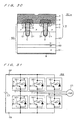
- FIG. 31 is a circuit diagram (in which 151 is typically added as a reference number for an IGBT) of a semiconductor device using the IGBTs151, 151a as switching elements.
- This semiconductor device 152 is formed as a three-phase inverter.
- Freewheel diodes 160 are parallel-connected to six IGBTs151, respectively. Freewheel diodes 160 are connected in such a direction that the reverse current of the corresponding IGBT151 is bypassed. The parallel connection in this direction is also referred to as "reverse parallel connection".
- IGBTs151 With respect to six IGBTs151, every two of them are series-connected.
- the collector electrode 8 of one of two series-connected IGBTs151 is connected to a higher potential power-supply terminal PP, and the emitter electrode 7 of the other is connected to a lower potential power-supply terminal NN. That is, three series circuits, each having two IGBTs151, are connected in parallel with each other between the higher potential power-supply terminal PP and the lower potential power-supply terminal NN.
- An external d-c power-supply 20 is connected to the higher potential power supply terminal PP and the lower potential power-supply terminal NN so as to supply a direct-current voltage.
- a connected portion of two IGBTs151 series-connected is connected to any one of output terminals U, V, W.
- a load 21 of, for example, a three-phase motor is connected to the three-phase output terminals U, V, W.
- a gate voltage V GE is externally applied to each of six gate electrodes 5 placed in six IGBTs151 individually so that six IGBTs151 are selectively turn on and off.
- three-phase alternating currents are supplied to the load 21.
- a single-phase inverter constituted by removing one of the three series circuits from the semiconductor device 152 of Fig. 31, has been conventionally used.
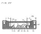
- Fig. 32 is a plan view of a conventionally-known semiconductor device that shows a specific construction of the semiconductor device (that is, a three-phase inverter) of Fig. 31, and Fig. 33 is a cross-sectional view of the semiconductor device taken along a cutting line X-X of Fig. 32.
- the circuit diagram of this semiconductor device 153 is shown in Fig. 31.
- the semiconductor device 153 comprises a housing 130, a heat-radiating plate 131 formed as one portion thereof, a substrate 135 placed on the heat-radiating plate 131, the six IGBTs151 placed on the substrate 135, the six freewheel diodes 160 also placed on the substrate 135, the higher potential power-supply terminal PP, the lower potential power-supply terminal NN, the three output terminals U, V, W, the six gate terminals G, a plurality of conductive wires w and a lid 133.
- the housing 130 (including the heat-radiating plate 131) and the lid 133 cooperatively form a closed space 132, and the substrate 135 is mounted in this closed space 132.
- the six IGBTs151 and the six freewheel diodes 160 are connected to the eleven terminals PP, NN, U, V, W, G through a number of conductive wires w.
- the conductive wires w are, for example, aluminum wires.
- Fig. 32 shows the semiconductor device 153 with its lid 133 removed.
- Fig. 34 is a plan view of the substrate 135, and also shows the IGBTs151 and the freewheel diodes 160 placed thereon.
- the substrate 135 comprises an insulating plate 136 and wiring patterns 137 placed thereon.
- the insulating plate 136 is fixed on the heat-radiating plate 131 (Fig. 33), and the IGBT151 and the freewheel diode 160 are mounted onto the wiring pattern 137, and electrically connected thereto. In this manner, both of the IGBT151 and the freewheel diode 160 are used in the form of a bear chip.
- the collector electrode 8 of each IGBT151 is connected to the cathode electrode of the corresponding freewheel diode 160 through the wiring pattern 137.
- the emitter electrode 7 of each IGBT151 and the anode electrode of the corresponding freewheel diode 160 are connected to each other through the conductive wire w.
- the emitter electrode 7 of one of the two IGBTs151 constituting a series circuit and the higher potential power-supply terminal PP are connected to each other by the conductive wire w
- the emitter electrode 7 of the other and any one of the three output terminals U, V, W, the collector electrode 8 of the one and any one of the three output terminals U, V, W, and the collector electrode 8 of the other and the lower potential power-supply terminal NN are respectively connected to each other by the wiring pattern 137 and the conductive wire w.
- the respective gate electrodes 5 of the six IGBTs151 and the corresponding gate terminals G are connected to each other by the conductive wires w.
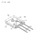
- Fig. 35 is an inner perspective view of a semiconductor device that shows another example of an applied apparatus.
- This semiconductor device 154 comprises a heat-radiating plate 125, an IGBT151 and a freewheel diode 160 that are placed thereon, a collector terminal 121, an emitter terminal 122, a gate terminal 123, conductive wires w and a sealing member 126 that seals all the elements except for the tip portions of the respective three terminals 121, 122, 123.
- a heat-radiating plate 125 which is made of cupper, and also referred to as a cupper frame, serves as a reinforcing member and a wiring pattern as well.
- the collector electrode 8 of the IGBT151 is connected to the cathode electrode of the corresponding freewheel diode 160 and the collector terminal 121 through the heat-radiating plate 125.
- the emitter electrode 7 of the IGBT151 and the anode electrode of the corresponding freewheel diode 160 are connected to each other by the conductive wire w.
- the emitter electrode 7 of the IGBT151 and the emitter terminal 122 are connected to each other by the conductive wire w, and the gate electrode 5 of the IGBT151 and the gate terminal 123 are also connected to each other by the conductive wire w.
- the freewheel diode 160 has been required so as to bypass a circulating current that forms a reverse current to the IGBT151.
- An inductive component included in the impedance of the inductive load (for example, represented by an induction L) stores energy in a magnetic field generated by a current. Therefore, a change in the current flowing through the induction L corresponds to a change in the energy to be stored.
- the induction L is exerted in such a way as to interrupt the change in current. Energy, accumulated in the induction L, is released to the IGBT151 that serves as a switching element to interrupt the current so that the current flowing through the induction L is attenuated.
- the energy accumulated in the induction L is so great that, if released instantaneously, it might easily break the IGBT151. Therefore, during the process in which the IGBT151 is turned off, the current flowing through the inductive load is circulated by bypassing it to the free-wheel diode 160 so that the current flowing through the inductive load is not changed by the switching.
- the semiconductor device 152 of Fig. 31 when one of the IGBTs151, which has been turned on to electrically connect the direct-current power supply 20 to the load 21 and supply a power-supply voltage to the load 21, is turned off, the current flowing through the load 21 is made to pass through the freewheel diode 160 and reversely flow through the direct-current power supply 20 by energy stored in the induction L of the load 21. As a result, a direct-current voltage that is reversed equivalently is applied to the load 21.
- the ratio between the time in which the IGBT151 is on and the time in which it is off is changed so that it is possible to control the average voltage to be applied to the load 21.
- this ratio to change in a sine-wave form, it is possible to supply to the load 21 a smooth alternating current without abruptly turning on or off the current flowing through the load 21 in synchronism with switching of the IGBT151.
- the inverter such as the semiconductor device 152 carries out the above-described operation so that, as shown in Figs. 31 to 33, it is necessary to connect the freewheel diode 160 in reverse-parallel to the corresponding IGBT151.
- a power MOSFET which has been used as a switching element since before the appearance of the IGBT151, inherently has a structure having a built-in reverse-parallel diode; therefore, it has been not necessary to connect the freewheel diodes 160 thereto in a separated manner.
- the power MOSFET has only a low current density, and is not suitable for the application with a great current.
- the IGBT which is suitable for the application with a great current, and has a construction in which an N + layer of the power MOSFET is replaced with the P + collector layer 91 so that a parasitic diode is formed between the P + collector layer 91 on the collector electrode 8 side and the N - base layers 92, 93.
- This tends to function as a high barrier with respect to a circulating current.
- the breakdown voltage of the parasitic diode is approximately 30 to 50 V, and this is an excessively high value so as to use the parasitic diode as a substitute for the reverse-parallel-connected freewheel diode. For this reason, if the freewheel diode 160 is not connected, IGBT151 might be damaged due to heat generated by a reverse voltage generated at the time of the circulation.
- the conventional IGBTs151, 151a are superior to the power MOSFETs in that the current density is great, they need to be connected to the freewheel diodes 160 when they are applied, and this causes extra costs and makes the structure of a semiconductor device serving as an application device complex, resulting in an increase in the size, an increase in the number of parts used for connections as well as an increase in processing costs.
- the present invention has been devised to solve the above-mentioned problems, and an object thereof is to provide an insulated gate bipolar transistor which can eliminate the necessity of connection to a freewheel diode, a semiconductor device using such a transistor, and manufacturing method thereof.
- the first aspect of the present invention is related to an insulated gate bipolar transistor comprising a semiconductor substrate having first and second major surfaces, a collector electrode which is located on said first major surface side of the semiconductor substrate, and an emitter electrode and a gate electrode that are located on said second major surface side, wherein the semiconductor substrate comprises a collector layer of a first conductive type that is exposed to the first major surface and connected to the collector electrode, and a base layer of a second conductive type that is formed on the collector layer and is not exposed to the first major surface, and wherein the base layer and the collector layer have a characteristic as a free-wheel diode.
- the second aspect of the present invention which relates to an insulated gate bipolar transistor in accordance with the first aspect, wherein a reverse voltage resistance, which is a minimum value of a collector-emitter voltage when a reverse current flows between the emitter electrode and the collector electrode, is set to not more than 5 times a collector-emitter saturated voltage.
- the third aspect of the present invention which relates to an insulated gate bipolar transistor in accordance with the second aspect, is designed so that the base layer comprises a base main body portion and a buffer layer that has a higher concentration of impurities than the base main body portion and is interpolated between the collector layer and the base main body portion, and a minimum value of a collector-emitter voltage when an avalanche current flows through a parasitic diode formed by the base layer and the collector layer is equivalent to the reverse voltage resistance.
- the fourth aspect of the present invention which relates to the insulated gate bipolar transistor in accordance with the second aspect, is designed so that the semiconductor substrate further comprises a reverse conductive-type layer of the second conductive type that is formed inside the collector layer so as not to be connected to the base layer, and selectively exposed to the first major surface, and connected to the collector electrode, and a minimum value of a collector-emitter voltage, that causes a punch through in which a depletion layer generated in a PN junction between the base layer and the collector layer reaches the reverse conductive-type layer, is equivalent to the reverse voltage resistance.
- the fifth aspect of the present invention which relates to the insulated gate bipolar transistor in accordance with the fourth aspect, is designed so that the collector layer comprises a low impurity concentration collector layer, and a high impurity concentration collector layer, the low impurity concentration collector layer comprises a portion of the collector layer sandwiched by the base layer and the reverse conductive-type layer, and the high impurity concentration collector layer has a concentration of impurities higher than the low impurity concentration collector layer.
- the sixth aspect of the present invention which relates to the insulated gate bipolar transistor in accordance with the fourth aspect, is designed so that the base layer comprises a base main body portion, and a buffer layer that has a higher concentration in impurities than the base main body portion, and is interpolated between the collector layer and the base main body portion.
- the seventh aspect of the present invention which relates to the insulated gate bipolar transistor in accordance with the second aspect, is designed so that the semiconductor substrate further comprises a reverse conductive-type layer of the second conductive type that is formed inside the collector layer so as not to be connected to the base layer, and selectively exposed to the first major surface and connected to the collector electrode, and a minimum value of a collector-emitter voltage when a parasitic bipolar transistor formed by the base layer, the collector layer and the reverse conductive type layer turns on, is equivalent to the reverse voltage resistance.
- the eighth aspect of the present invention which relates to the insulated gate bipolar transistor in accordance with the seventh aspect, is designed so that the collector layer comprises a low impurity concentration collector layer, and a high impurity concentration collector layer, and the low impurity concentration collector layer comprises a portion of the collector layer sandwiched by the base layer and the reverse conductive-type layer, and the high impurity concentration collector layer has a concentration of impurities higher than the low impurity concentration collector layer.
- the ninth aspect of the present invention which relates to the insulated gate bipolar transistor in accordance with the seventh aspect, is designed so that the base layer comprises a base main body portion, and a buffer layer that has a higher concentration in impurities than the base main body portion, and is interpolated between the collector layer and the base main body portion.
- the tenth aspect of the present invention which relates to the insulated gate bipolar transistor in accordance with the second aspect, is designed so that the reverse voltage resistance is not more than 10 V.
- a semiconductor device comprises the insulated gate bipolar transistor in accordance with the first aspect, a housing in which the insulated gate bipolar transistor is mounted, and three terminals each of which is attached to said housing with its one portion protruding from said housing toward the exterior, and which are electrically connected to said gate electrode, said emitter electrode and said collector electrode of the insulated gate bipolar transistor, respectively.
- the semiconductor device which relates to the eleventh aspect is designed so that the gate electrode, the emitter electrode and the collector electrode are electrically connected to the three terminals through conductive wires, respectively.
- the thirteenth aspect of the present invention which relates to the semiconductor device in accordance with the eleventh aspect, further comprises the insulated gate bipolar transistor serving as a first transistor, three insulated gate bipolar transistors having the same structure as the first transistor and serving as second through fourth transistors, the three-terminals serving as first to third terminals, and five terminals each of which is attached to the housing with one portion thereof protruding from the housing toward the exterior, the five terminals serving as fourth to eighth terminals, wherein the first and second transistors are series-connected, the third and fourth transistors are series-connected, the first terminal is electrically connected to the collector electrodes of the first and third transistors, the second terminal is electrically connected to connecting sections of the first and second transistors, the third terminal is electrically connected to the gate electrode of the first transistor, the fourth terminal is electrically connected to the emitter electrodes of the second and fourth transistors, the fifth terminal is electrically connected to connecting sections of the third and fourth transistors, and the sixth through eighth terminals are electrically connected to the gate electrodes of the second through
- the fourteenth aspect of the present invention which relates to the semiconductor device in accordance with the thirteenth aspect, further comprises an inductive load connected to the second terminal and the fifth terminal.
- the fifteenth aspect of the present invention which relates to a semiconductor device, comprises the insulated gate bipolar transistor in accordance with the first aspect, a sealing member that seals the insulated gate bipolar transistor, and three terminals each of which is sealed by the sealing member with one portion thereof protruding from the sealing member toward the exterior, the three terminals electrically connected to the gate electrode, the emitter electrode and the collector electrode of the insulated gate bipolar transistor, respectively.
- a manufacturing method of an insulated gate bipolar transistor which comprises a semiconductor substrate having first and second major surfaces, a collector electrode that is located on the first major surface side of the semiconductor substrate, and an emitter electrode and a gate electrode that are located on the second major surface side, comprising the steps of:(a) forming the semiconductor substrate so as to provide a collector layer of a first conductive type that is exposed to the first major surface and a base layer of a second conductive type that is formed on the collector layer and is not exposed to the first major surface, and (b) forming the collector electrode on the first major surface so as to be connected to the collector layer, wherein in the step (a), the semiconductor substrate is formed so that the base layer and the collector layer are allowed to have a characteristic as a freewheel diode.
- the seventeenth aspect of the present invention which relates to the manufacturing method of an insulated gate bipolar transistor in accordance with the sixteenth aspect, is designed so that in the step (a), the semiconductor substrate is formed in such a manner that a reverse voltage resistance, which is a minimum value of a collector-emitter voltage when a reverse current flows between the emitter electrode and the collector electrode, is set to not more than 5 times the collector-emitter saturated voltage.
- the eighteenth aspect of the present invention which relates to the manufacturing method of an insulated gate bipolar transistor in accordance with the seventeenth aspect, is designed so that in the step (a), the base layer comprises a base main body portion and a buffer layer that has a higher concentration in impurities than the base main body portion and is interpolated between the collector layer and the base main body portion, and the semiconductor substrate is formed so that a minimum value of a collector-emitter voltage when an avalanche current flows through a parasitic diode formed by the base layer and the collector layer is equivalent to the reverse voltage resistance.
- the nineteenth aspect of the present invention which relates to the manufacturing method of an insulated gate bipolar transistor in accordance with the seventeenth aspect, is designed so that in the step (a), the semiconductor substrate further comprises a reverse conductive-type layer of the second conductive type that is formed inside the collector layer so as not to be connected to the base layer, and selectively exposed to the first major surface, and connected to the collector electrode, and the semiconductor substrate is formed so that a minimum value of a collector-emitter voltage that causes a punch through in which a depletion layer generated in a PN junction between the base layer and the collector layer reaches the reverse conductive-type layer is equivalent to the reverse voltage resistance.
- the twentieth aspect of the present invention which relates to the manufacturing method of the insulated gate bipolar transistor in accordance with the nineteenth aspect, is designed so that in the above-mentioned step (a), the collector layer comprises a low impurity concentration collector layer and a high impurity concentration collector layer, and in the semiconductor substrate thus formed, the low impurity concentration collector layer includes a portion of the collector layer sandwiched by the base layer and the reverse conductive-type layer, and the high impurity concentration collector layer has a concentration of impurities higher than the low impurity concentration collector layer.
- the twenty-first aspect of the present invention which relates to the manufacturing method of the insulated gate bipolar transistor in accordance with the nineteenth aspect, is designed so that in the step (a), the semiconductor substrate is formed in such a manner that the base layer comprises a base main body portion and a buffer layer that has a higher concentration in impurities than the base main body portion, and is interpolated between the collector layer and the base main body portion.
- the twenty-second aspect of the present invention which relates to the manufacturing method of an insulated gate bipolar transistor in accordance with the seventeenth aspect, is designed so that in the step (a), the semiconductor substrate further comprises a reverse conductive-type layer of the second conductive type that is formed inside the collector layer so as not to be connected to the base layer, and selectively exposed to the first major surface, and connected to the collector electrode, and the semiconductor substrate is formed so that a minimum value of a collector-emitter voltage when a parasitic bipolar transistor formed by the base layer, the collector layer and the reverse conductive type layer turns on is equivalent to the reverse voltage resistance.
- the twenty-third aspect of the present invention which relates to the manufacturing method of the insulated gate bipolar transistor in accordance with the twenty-second aspect, is designed so that in the step (a), the semiconductor substrate is formed in such a manner that the collector layer comprises a low impurity concentration collector layer and a high impurity concentration collector layer, and in this structure, the low impurity concentration collector layer includes a portion of the collector layer sandwiched by the base layer and the reverse conductive-type layer, and the high impurity concentration collector layer has a concentration of impurities higher than the low impurity concentration collector layer.
- the twenty-fourth aspect of the present invention which relates to the manufacturing method of the insulated gate bipolar transistor in accordance with the twenty-second aspect, is designed so that in the step (a), the semiconductor substrate is formed in such a manner that the base layer comprises a base main body portion and a buffer layer that has a higher concentration in impurities than the base main body portion, and is interpolated between the collector layer and the base main body portion.
- the twenty-fifth aspect of the present invention which relates to the manufacturing method of the insulated gate bipolar transistor in accordance with the seventeenth aspect, is designed so that in the step (a), the semiconductor substrate is formed in such a manner that the reverse voltage resistance is set to not more than 10 V.
- a manufacturing method of a semiconductor device comprises the steps of: (A) obtaining a housing having three terminals each of which is attached thereto with its one portion protruding toward the exterior, (B) executing the manufacturing method of the insulated gate bipolar transistor according to claim 16 to thereby obtain the insulated gate bipolar transistor, (C) mounting the insulated gate bipolar transistor in the housing, and (D) electrically connecting the three terminals to the gate electrode, the emitter electrode and the collector electrode of the insulated gate bipolar transistor, respectively.
- the step (D) further comprises a step (D-1) of electrically connecting the gate electrode, the emitter electrode and the collector electrode to the three terminals respectively through conductive wires.
- the step (A) is arranged so that the housing is obtained with the three-terminals serving as the first to third terminals, and allowed to further include five terminals each of which is attached thereto with its one portion externally sticking out as the fourth through eighth terminals;
- the step (B) is arranged so that the insulated gate bipolar transistor is obtained as the first transistor with three insulated gate bipolar transistors having the same structure as the first transistor being obtained as the second through fourth transistors;
- the step (C) is arranged so that, in addition to the first transistor, the second through fourth transistors are mounted in the housing; and the step (D) further comprises the steps of: (D1) connecting the first and second transistors in series with each other; (D2) connecting the third and fourth transistors in series with each other; (D3) electrically connecting the first terminal to the collector electrodes of the first and third transistors; (D4) electrically connecting the second terminal to the connecting sections of
- the manufacturing method of the semiconductor device in accordance with the twenty-eighth aspect further comprises a step of (E) connecting an inductive load to the second terminal and the fifth terminal.
- a manufacturing method of a semiconductor device comprises the steps of: (A) obtaining three terminals, (B) executing the manufacturing method of the insulated gate bipolar transistor according to claim 16 to thereby obtain the insulated gate bipolar transistor, (C) electrically connecting the three terminals to the gate electrode, the emitter electrode and the collector electrode of the insulated gate bipolar transistor, respectively, and (D) sealing the insulated gate bipolar transistor and the three terminals in such a manner that one portion of each of the three terminals is allowed to protrude toward the exterior.
- the present invention which has the arrangements as described above, makes it possible to provide the following effects.
- the base layer and the collector layer have the characteristic of the freewheel diode, it is not necessary to externally connect the freewheel diode upon application thereof.
- the insulated gate bipolar transistor related to the second aspect of the present invention since the reverse voltage resistance is reduced to not more than 5 times the collector-emitter saturated voltage, the circulating current is allowed to flow through itself without the necessity of any special heat-radiating design even when an inductive load is connected thereto.
- the reverse voltage resistance is determined by the avalanche breakdown of the parasitic diode, it is possible to easily suppress the collector-emitter saturated voltage to a low level by increasing the concentration of impurities of the collector layer.
- the buffer layer since the buffer layer is installed, it is possible to make the base layer thinner, and consequently to further reduce both of the collector-emitter saturated voltage and the reverse voltage resistance.
- the reverse voltage resistance is determined by a punch through voltage, and it becomes possible to set the reverse voltage resistance to a low level.
- the collector layer comprises the high impurity concentration collector layer, it becomes possible to suppress the collector-emitter saturated voltage to a low level by compensating for the reduction in the amount of injection of holes due to the installed reverse conductive-type layer.
- the buffer layer since the buffer layer is installed, it is possible to make the base layer thinner, and consequently to further reduce both of the collector-emitter saturated voltage and the reverse voltage resistance.
- the reverse voltage resistance is determined by a turning-on of the parasitic bipolar transistor so that it becomes possible to easily set the reverse voltage resistance to a low level.
- the collector layer comprises the high impurity concentration collector layer, it becomes possible to suppress the collector-emitter saturated voltage to a low level by compensating for the reduction in the amount of injection of holes due to the installed reverse conductive-type layer.
- the buffer layer since the buffer layer is installed, it is possible to make the base layer thinner, and consequently to further reduce both of the collector-emitter saturated voltage and the reverse voltage resistance.
- the reverse voltage resistance is set to not more than 10 V, it is possible to reduce the amount of heat generation due to the reverse current to a low level, even in the case of a collector-emitter saturated voltage exceeding 2 V.
- the insulated gate bipolar transistor is mounted in a housing, it is possible to provide a convenient means in which the insulated gate bipolar transistor is connected to a power supply and a load and utilized. Moreover, since the insulated gate bipolar transistor in accordance with the first aspect of the present invention that requires no freewheel diodes is utilized, it is possible to miniaturize the device, and also to cut manufacturing costs.
- each electrode of the insulated gate bipolar transistor and each terminal are electrically connected through the conductive wire, it is possible to simplify the manufacturing process, and consequently to further reduce the manufacturing cost. In particular, since no freewheel diodes are required, it is possible to reduce the number of conductive wires and the number of connecting processes.
- the insulated gate bipolar transistor in accordance with the first aspect of the present invention that requires no freewheel diodes is utilized, it is possible to achieve a small-size inverter that is inexpensive and easily used.
- the insulated gate bipolar transistor is sealed by the sealing member, it is possible to provide a convenient means in which the insulated gate bipolar transistor is connected to a power supply and a load and utilized. Moreover, since the insulated gate bipolar transistor in accordance with the first aspect of the present invention that requires no freewheel diodes is utilized, it is possible to miniaturize the device, and also to cut manufacturing costs.
- the base layer and collector layer are allowed to have the characteristic as the freewheel diode, it is possible to obtain the insulated gate bipolar transistor that requires no externally connected freewheel diode upon application thereof.
- the reverse voltage resistance is reduced to not more than 5 times the collector-emitter saturated voltage, it is possible to provide the insulated gate bipolar transistor in which the circulating current is allowed to flow through itself without the necessity of any special heat-radiating design even when an inductive load is connected thereto.
- the semiconductor substrate is formed so that the reverse voltage resistance is determined by the avalanche breakdown of the parasitic diode, it is possible to easily suppress the collector-emitter saturated voltage to a low level by increasing the concentration of impurities of the collector layer.
- the buffer layer is installed, it is possible to make the base layer thinner, and consequently to further reduce both of the collector-emitter saturated voltage and the reverse voltage resistance.
- the semiconductor substrate is formed so that the reverse conductive-type layer is formed inside the collector layer and the reverse voltage resistance is consequently determined by a punch through voltage, it becomes possible to set the reverse voltage resistance to a low level.
- the semiconductor substrate is formed so that the collector layer comprises the high impurity concentration collector layer, it becomes possible to suppress the collector-emitter saturated voltage to a low level by compensating for the reduction in the amount of injection of holes due to the installed reverse conductive-type layer.
- the buffer layer since the buffer layer is installed, it is possible to make the base layer thinner, and consequently to further reduce both of the collector-emitter saturated voltage and the reverse voltage resistance.
- the semiconductor substrate is formed so that the reverse conductive-type layer is formed inside the collector layer with the reverse voltage resistance being determined by a turning-on of the parasitic bipolar transistor, it becomes possible to easily set the reverse voltage resistance to a low level.
- the semiconductor substrate is formed so that the collector layer has the high impurity concentration collector layer, it becomes possible to suppress the collector-emitter saturated voltage to a low level by compensating for the reduction in the amount of injection of holes due to the installed reverse conductive-type layer.
- the buffer layer since the buffer layer is installed, it is possible to make the base layer thinner, and consequently to further reduce both of the collector-emitter saturated voltage and the reverse voltage resistance.
- the reverse voltage resistance is set to not more than 10 V, it is possible to reduce the amount of heat generation due to the circulating current to a low level, even in the case of the collector-emitter saturated voltage exceeding 2 V.
- the insulated gate bipolar transistor is mounted in the housing, it is possible to provide the convenient means in which the insulated gate bipolar transistor is connected to a power supply and a load and utilized. Moreover, since the insulated gate bipolar transistor in accordance with the first aspect of the present invention that requires no freewheel diodes is utilized, it is possible to miniaturize the device, and also to cut manufacturing costs.
- each electrode of the insulated gate bipolar transistor and each terminal are electrically connected through the conductive wire, it is possible to simplify the manufacturing process, and consequently to further reduce the manufacturing cost. In particular, since no freewheel diodes are required, it is possible to reduce the number of conductive wires and the number of connecting processes.
- the insulated gate bipolar transistor in accordance with the first aspect of the present invention that requires no freewheel diodes is utilized, it. is possible to achieve a small-size inverter that is inexpensive and easily used.
- the insulated gate bipolar transistor is sealed by the sealing member, it is possible to provide the convenient semiconductor device in which the insulated gate bipolar transistor is connected to a power supply and a load, and utilized. Moreover, since the insulated gate bipolar transistor in accordance with the first aspect of the present invention that requires no freewheel diodes is utilized, it is possible to miniaturize the device, and also to cut manufacturing costs.
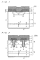
- Fig. 1 is a front cross-sectional view of an IGBT in accordance with a first preferred embodiment of the present invention.
- This IGBT101 comprises a semiconductor substrate 1 having first and second major surfaces.
- This semiconductor substrate 1 which is a silicon substrate, comprises a P + collector layer 11 that is a P + substrate that is exposed to the first major surface, an N + buffer layer 12 formed thereon, an N - base layer 13 that is formed thereon with a lower concentration of impurities than the N + buffer layer 12, a P base region 2 that is formed by selectively diffusing P-type impurities on the second major surface to which the N - base layer 13 is exposed, and an N + source region 3 that is formed as a region shallower than the P base region 2 by selectively diffusing N-type impurities with a high concentration inside this P base region 2.
- the concentration of the N-type impurities is set higher than that of the N + buffer layer 92 of the conventional IGBT151 (see Fig. 29).
- An emitter electrode 7 is further formed on the upper major surface of the semiconductor substrate 1 in a manner so as to connect with one portion of the surface of the N + source region 3 and a center area of the surface of the P base region 2.
- the gate electrode 5 and the emitter electrode 7 are insulated from each other by an interlayer insulating film 6.
- the N - base layer 13, the P base region 2 and the N + source region 3, which are formed on the second major surface side of the semiconductor substrate 1, correspond to a semiconductor portion of an MOS transistor.
- the portion having the same construction as the MOS transistor formed on the second major surface side of the semiconductor substrate 1. is referred to as an MOS construction M.
- a portion of the surface of the P base region 2, which is located right below the gate electrode 5, and sandwiched by the source region 3' and the N - base layer 13, that is, a portion at which the gate electrodes 5 face each other with the gate insulating film 4 sandwiched in between, corresponds to a channel region CH of the MOS structure M.
- the P base region 2 and the N + source region 3 are formed by selectively implanting and diffusing impurities by using the gate electrode 5 as a mask. That is, since the P base region 2 and the N + source region 3 form a double diffusion region, the MOS structure M forms one example of Double Diffused MOS (referred to simply as a DMOS).
- a collector electrode 8 to be connected to the P + collector layer 11 is formed on the first major surface of the semiconductor substrate 1.
- Fig. 2 is a front cross-sectional view of an insulated gate bipolar transistor in accordance with another example of the first preferred embodiment.
- This IGBT101a is typically different from the IGBT101 in its MOS structure M formed on the second major surface side of the semiconductor substrate 1.
- a gate electrode 5 is buried inside the gate insulating film 4.
- an N + buffer layer 12 is set to have a higher concentration in N-type impurities than that of the N + buffer layer 92 of the conventional IGBT151a (Fig. 30).
- each of the planar IGBT101 of Fig. 1 and the trench-type IGBT101a of Fig. 2 comprises a P + collector layer 11 that is exposed to the first major surface of the semiconductor substrate 1, the N base layers 12, 13 formed thereon, the MOS structure M (including one portion of the N - base layer 13) formed on the second major surface and a collector electrode 8 that is formed on the first major surface and connected to the P + collector layer 11.
- a number of cells, shown in Fig. 1 or 2 are reciprocally arranged along the major surfaces of the semiconductor substrate 1 so that a greater current rate is obtained by this arrangement. In Fig. 1, one cell is drawn, and in Fig. 2, two cells are drawn.
- a collector voltage referred to as a collector voltage
- a gate-emitter voltage referred to as a gate voltage
- V GE with a positive bias having a predetermined level is applied between the emitter electrode 7 and the gate electrode 5; that is, upon turning on the gate, a conductive type of the channel region CH is inverted from a P type to an N type.
- a channel serving as a carrier path is formed in the channel region CH. Electrons are injected from the emitter electrode 7 to the N - base layer through this channel.
- the electrons thus injected make the P + collector layer 11 and the N base layers 12, 13 forwardly biased so that holes are injected to the N base layers 12, 13 from the P + collector layer 11.
- the resistance of N - base layer 12 drops greatly so that the current capacity of IGBT101, 101a is increased.
- a collector voltage V CE which is applied between the emitter electrode 7 and the collector electrode 8, is determined by a thickness of the N - base layer 13 and its concentration of impurities.
- a parasitic diode D is formed in an equivalent manner by the N base layers 12, 13 and the P + collector layer 11.
- the concentration of N-type impurities is set sufficiently higher than the N + buffer layer 92 of the conventional IGBT151, 151a; therefore, the breakdown voltage of parasitic diode D, which is determined by the P + collector layer 11 and the N + buffer layer 12, is suppressed to a low level.
- This breakdown voltage determines the reverse voltage resistance of IGBTs101, 101a.
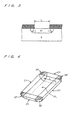
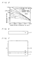
- Figs. 3 to 5 are drawings quoted from page 105 of "Semiconductor Device” written by S.M.Sze (published by “Sangyo Tosho”, in 1987)(translation of S.M.Sze, “Semiconductor Devices-Physics and Technology-", published by Bell Telephone Laboratories, Inc. 1985).
- Fig. 3 shows a curved surface of a PN junction that is generated at the end portion of a diffusion mask in a planar diffusion process, and a symbol r j represents a curvature radius of the curved surface.
- Fig. 3 shows a curved surface of a PN junction that is generated at the end portion of a diffusion mask in a planar diffusion process, and a symbol r j represents a curvature radius of the curved surface.
- Fig. 4 shows a diffusion region that is formed by using a diffusion mask having a rectangular shape
- a symbol PL represents a plane region
- a symbol CY represents a cylinder shaped region
- a symbol SP represents a spherical region.
- Fig. 3 corresponds to a longitudinal cross-sectional view showing the diffusion region of Fig. 4.
- Fig. 5 represents the relation between the breakdown voltage V B and the concentration of impurities N B in the PN junction shown in Figs. 3 and 4.
- the breakdown voltage V B means a reverse voltage that causes an avalanche breakdown in the PN junction.
- the graph of Fig. 5 shows that it is possible to reduce the breakdown voltage between the N + buffer layer 12 and the P + collector layer 11 to not more than 10 V, by adjusting the concentration of impurities of N + buffer layer 12 (so as to set to not less than 5 ⁇ 10 17 cm -3 ).
- a power factor of a normal inductive load such as a motor is set to a high level such as not less than 0.8; therefore, in a normal inverter that is connected to such an inductive load, and used, the average value of currents flowing through the IGBT in a forward direction becomes not less than 5 times the average value of the circulating current.
- the reverse voltage resistance of the IGBT is set to a voltage of not more than 5 times a voltage between the collector electrode 8 and the emitter electrode 7 at the time when the IGBT is on, that is, no more than 5 times a collector-emitter saturated voltage V CE (sat), it becomes possible to allow the circulating current to pass through the IGBT itself as a reverse current without causing a damage due to heat generation, even when a freewheel diode is not connected to the IGBT and the heat radiating structure of the conventional IGBT, as it is, is adopted.
- the collector-emitter saturated voltage V CE(sat) is approximately 2 V; therefore, if the reverse voltage resistance of the IGBT can be set to not more than 10 V, it becomes possible to use the IGBT as a switching element in an inverter without the necessity of freewheel diode.
- the graph of Fig. 5 shows that the IGBTs101, 101a can be designed as the IGBT that is applicable without using the freewheel diode, by setting the concentration of impurities in the N + buffer layer 12 to a sufficiently high value.
- the IGBTs101, 101a having such an arrangement are allowed to function in a manner equivalent to IGBTs151, 151a in which freewheel diodes, each having a forward voltage V F of not more than 10 V, are connected in reverse-parallel with each other.
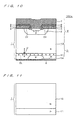
- Figs. 6 and 7 are manufacturing process drawings that show one example of a manufacturing method of the IGBT101, 101a.
- a silicon substrate 11 of a P + type is prepared (Fig. 6).
- an N + buffer layer 12 and an N - base layer 13 are formed in this order (Fig. 7) on a major surface of the silicon substrate 11.
- the N + buffer layer 12 and the N - base layer 13 may be formed by implanting and diffusing impurities or by utilizing the epitaxial growth.
- a portion of the silicon substrate 11 that is left as a P + type semiconductor layer after the N + buffer layer 12 and the N - base layer 13 have been formed corresponds to the P + collector layer 11.
- the silicon substrate 11 In the case when the epitaxial growth is utilized in both of the formation processes of the N + buffer layer 12 and the N - base layer 13, the silicon substrate 11, as it is, forms the P + collector layer 11. In the case of the application of implantation and diffusion of impurities also, the major portion of silicon substrate 11 forms the P + collector layer 11. Therefore, the silicon substrate 11 is represented by the same reference number as the P + collector layer 11.
- the collector electrode 8 is formed on the first major surface of the semiconductor substrate 1 to which the P + collector layer 11 is exposed (Fig. 1 or Fig. 2). Since the processes for forming the MOS structure M have been conventionally known, the detailed description thereof is omitted.
- the shape (including the size) of respective semiconductor layers and the concentration of impurities are controlled so that the reverse voltage resistance of each of the IGBTs101, 101a is set to not more than 5 times the collector-emitter saturated voltage V CE(sat) , more preferably, not more than 10 V.
- the concentration of impurities of the N + buffer layer 12 is adjusted.
- Fig. 8 is a manufacturing process drawing that shows another example of a method for manufacturing the IGBTs101, 101a.
- an N - type silicon substrate 13 is prepared.
- an N + buffer layer 12 and a P + collector layer 11 are formed in this order on a major surface of the silicon substrate 13 to form the same structure as that of Fig. 7.
- the N + buffer layer 12 and the P + collector layer 11 may be formed by implanting and diffusing impurities or utilizing the epitaxial growth.
- the above-mentioned processes for forming the MOS structure M and the collector electrode 8, which have been described by reference to Fig. 1 or Fig. 2 are carried out to form the IGBTs101, 101a.
- the above-mentioned processes are the same as those manufacturing processes of the conventional IGBTs151, 151a, except that the shape of the respective semiconductor layers and the concentration of impurities are controlled so that the reverse voltage resistance of each of the IGBTs101, 101a is set to not more than 5 times the collector-emitter saturated voltage V CE(sat) . That is, the IGBTs101, 101a can be manufactured without the necessity of any special complex processes in comparison with the conventional IGBTs151, 151a.
- Fig. 9 is a front cross-sectional view that shows an IGBT in accordance with a second preferred embodiment of the present invention.
- those parts that are the same as or correspond to (those parts having the same functions as) those of the device in accordance with the first preferred embodiment shown in Fig. 1 and Fig. 2 are represented by the same reference numbers, and the description thereof is omitted.
- an IGBT102 shown in Fig. 9, is typically distinct from the IGBT101 of Fig. 1 in that the semiconductor substrate 1 comprises an N + reverse conductive-type layer 14 (for example, referred to as a reverse conductive-type layer, since it has a conductive type reversed to the P + collector layer 11 on the periphery thereof).
- N + reverse conductive-type layer 14 for example, referred to as a reverse conductive-type layer, since it has a conductive type reversed to the P + collector layer 11 on the periphery thereof.
- the N + reverse conductive-type layer 14 is selectively exposed to the first major surface of the semiconductor substrate 1, and formed inside the P + collector layer 11 so as to be shallower than the P + collector layer 11. Therefore, the N + reverse conductive-type layer 14 and the N base layers 12, 13 are separated from each other by the P + collector layer 11.
- a depletion layer DL is generated at a PN junction of the parasitic diode D.
- a thickness of the P + collector layer 11 (in particular, a thickness of a portion making the N + reverse conductive-type layer 14 and the N + buffer layer 12 separate from each other) and the concentration of impurities are adjusted so that, when this reverse voltage is not more than 5 times (more preferably, not more than 10 V) the collector-emitter saturated voltage V CE(sat) , the depletion layer DL is allowed to reach the N + reverse conductive-type layer 14 (that is, a punch through occurs).
- the reverse voltage resistance of IGBT102 is regulated by the punch through so that the reverse voltage resistance is set to a value not more than 5 times the collector-emitter saturated voltage V CE(sat) . Therefore, in the same manner as the IGBTs101, 101a of the first preferred embodiment, it becomes possible to use the IGBT102 as a switching element in an inverter without the necessity of connection to the freewheel diode.
- the basic switching operation serving as the IGBT is unchanged from the operation of conventional IGBTs151, 151a. Since the N + reverse conductive-type layer 14 is installed, the injection efficiency of holes from the P + collector layer 11 is reduced. However, in general, a life time killer is introduced to the N - base layer and the N + buffer layer 12 so that by adjusting the amount of the introduction of the life time killer, it is possible to compensate for a change in characteristics due to the reduction of the injection efficiency of holes.
- the N + buffer layer 12 does not necessarily give an essential effect to the punch through. Therefore, even in a structure form in which the N + buffer layer 12 is omitted as shown as an IGBT102a in Fig. 10, it is possible to obtain the same effect as the IGBT102 with respect to the reverse voltage resistance.
- the IGBT102 having the N + buffer layer 12 makes it possible to provide a thinner N - base layer 13.
- the MOS structure M of the IGBT102, 102a may be changed to a trench type, and the same effect is obtained with respect to the reverse voltage resistance.
- IGBTs102, 102a The structure of IGBTs102, 102a is unchanged from the structure that has been conventionally adopted in IGBTs with high voltage resistance and generally referred to as "non-punch through structure", except for characteristics in the thickness of the P + collector layer 11 and the concentration of impurities. Therefore, in a method for manufacturing the IGBTs12, 102a also, the conventional method as it is may be adopted except that the thickness of the P + collector layer 11 and the concentration of impurities are controlled, as will be described below.
- an N - type silicon substrate 13 is prepared as shown in Fig. 8.
- the P + layer 11 is formed on one major surface of the silicon substrate 13 by carrying out a process shown in Fig. 11.
- the P + layer 11 may be formed by implanting and diffusing impurities or utilizing the epitaxial growth.
- the N + reverse conductive-type layer 14 is formed by selectively implanting and diffusing N type impurities on the major surface to which the P + layer 11 is exposed.
- the N + buffer layer 12 and the P + collector layer 11 are formed on one major surface of the silicon substrate 13 in this order, as shown in Fig. 13 in place of Fig. 12, and N-type impurities are then selectively implanted and diffused on the major surface to which the P + layer 11 is exposed so that the N + reverse conductive-type layer 14 is formed.
- Both of the N + buffer layer 12 and the P + collector layer 11 may be formed by implanting and diffusing impurities or utilizing the epitaxial growth.
- the MOS structure M and the collector electrode 8 are formed so that the IGBTs102, 102a are completed (Fig. 9 or Fig. 10).
- Figs. 14 and 15 are front cross-sectional views of IGBTs in accordance with the third preferred embodiment of the present invention.
- An IGBT103 shown in Fig. 14 and an IGBT103a shown in Fig. 15 are assembled in the same manner as the IGBTs102 and 102a of the second preferred embodiment, respectively, except for differences in the thickness of the P + collector layer 11 and the concentration of impurities.
- the N base layers 12, 13, the P + collector layer 11 and the N + reverse conductive-type layer 14 constitute an NPN-type parasitic bipolar transistor Q in an equivalent manner.
- An emitter of this parasitic bipolar transistor Q is connected to the collector electrode 8, and a base is connected to the collector electrode 8 through a resistor R.
- the resistor R corresponds to a resistance component belonging to a portion of the P + collector layer 11 sandwiched by the N base layers 12, 13 and the N + reverse conductive-type layer 14.
- the thickness of the P + collector layer 11 (in particular, the thickness of a portion making the N + reverse conductive-type layer 14 and the N + buffer layer 12 separate from each other) and the concentration of impurities are adjusted so that, when a reverse voltage to be applied between the collector electrode 8 and the emitter electrode 7 is not more than 5 times (more preferably, not more than 10 V) the collector-emitter saturated voltage V CE(sat) , a parasitic bipolar transistor Q is turned on.
- the reverse voltage resistance of IGBT103, 103a is regulated by tuning-on of the parasitic bipolar transistor Q, and set to a value not more than 5 times the collector-emitter saturated voltage V CE(sat) . Therefore, in the same manner as the IGBT101, 101a of the first preferred embodiment, the IGBT102 may be used as an inverter without the necessity of connection to the freewheel diode.
- the N + buffer layer 12 does not necessarily give an essential effect to the turning-on of parasitic bipolar transistor Q. Therefore, the IGBTs103 and 103a are allowed to mutually obtain the same effect with respect to the reverse voltage resistance.
- the IGBT103 having the N + buffer layer 12 makes it possible to provide the thinner N - base layer 13.
- the MOS structure M of the IGBT103, 103a may be changed to a trench type, and the same effects are obtained with respect to the reverse voltage resistance.
- the structure of IGBTs103, 103a is the same as the structure of IGBTs102, 102a except for characteristics in the thickness of the P + collector layer 11 and the concentration of impurities. Therefore, the IGBTs103, 103a are easily manufactured by using the same processes as the manufacturing processes of the IGBT102, 102a. For this reason, with respect to the manufacturing method of the IGBT103, 103a, the detailed description thereof is omitted.
- Figs. 16 and 17 are front cross-sectional views of an IGBT in accordance with the fourth preferred embodiment of the present invention.
- An IGBT104 shown in Fig. 16 is characterized in that a P + type diffusion layer 15 having a high concentration of impurities is selectively formed in the P + collector layer 11 of the IGBT102 in accordance with the second preferred embodiment or the IGBT103 in accordance with the third preferred embodiment.
- an IGBT104a shown in Fig. 17 is characterized in that a P + type diffusion layer 15 having a high concentration of impurities is selectively formed in the P + collector layer 11 of the IGBT102a in accordance with the second preferred embodiment or the IGBT103a in accordance with the third preferred embodiment.
- the P + collector layer 11 comprises a P + layer 11a having a low concentration of impurities (for example, referred to as a "low-impurity-concentration collector layer”) and a P + diffusion layer 15 having a high concentration of impurities (for example, referred to as a "high-impurity-concentration collector layer”).
- the P + diffusion layer 15 is formed in a manner adjacent to the N + reverse conductive-type layer 14 along the first major surface of the semiconductor substrate 1 by selectively diffusing P-type impurities in a portion of the first major surface of the semiconductor substrate 1 to which no N + reverse conductive-type layer 14 is exposed.
- the P + layer 11a corresponds to a portion of the P + collector layer 11 having no P + diffusion layer 15 formed thereon, that is, a portion sandwiched by the N + reverse conductive-type layer 14 and the N base layers 12, 13.
- the basic operation of the IGBTs104, 104a is the same as that of the IGBTs102, 102a, 103, 103a in accordance with the second or third preferred embodiment.
- the N + reverse conductive-type layer 14 is formed inside the P + collector layer 11 with the result that the concentration of P-type impurities of the P + collector layer 11 needs to be reduced to a low level in comparison with the conventional IGBTs151, 151a.
- the resulting problem is that the amount of injection of holes from the P + collector layer 11 becomes low, causing the collector-emitter saturated voltage V CE(sat) to become higher.
- the P + diffusion layer 15 having a high concentration of impurities is formed in a region out of the P + collector layer 11 in which no N + reverse conductive-type layer 14 is formed; therefore, it is possible to increase the amount of injection of holes from the P + collector layer 11 without impairing the function of N + reverse conductive-type layer 14, and consequently to reduce the collector-emitter saturated voltage V CE(sat) .
- the IGBTs104, 104a are easily manufactured by adding a process for forming the P + diffusion layer 15 to a method for forming the IGBTs102, 102a, 103, 103a.
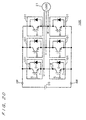
- Fig. 20 is a circuit diagram (in which 101 is typically added as a reference number for an IGBT) of a semiconductor device using IGBTs101 to 104, 101a to 104a as switching elements.
- This semiconductor device 105 is formed as a three-phase inverter.
- the P + collector layer 11 and the N base layers 12, 13 have characteristics as a freewheel diode so that the IGBT101 itself is allowed to function as a freewheel diode in an equivalent manner; therefore, it is not necessary to connect a freewheel diode 160 (Fig. 31) thereto in a separate manner.
- Fig. 20 also shows a freewheel diode in which the IGBT101 itself functions in an equivalent manner.
- the six IGBTs101 are series-connected two by two.
- a collector electrode 8 of one of the series-connected two IGBTs101 is connected to a higher potential power-supply terminal PP, and an emitter electrode 7 of the other is connected to a lower potential power-supply terminal NN. That is, three series circuits, each having the two IGBTs101, are connected in parallel with each other between the higher potential power-supply terminal PP and the lower potential power-supply terminal NN.
- An external direct-current power-supply 20 is connected to the higher potential power-supply terminal PP and the lower potential power-supply terminal NN so that a direct current voltage is supplied thereto.
- the connecting portion of the two IGBTs101 series-connected is connected to any one of output terminals U, V, W.
- a load 21 such as a three-phase motor is connected to the three-phase output terminals U, V, W.
- it is possible to form a single phase inverter by removing one of the three series circuits from the semiconductor device 105 of Fig. 20.
- Gate voltage V GE is externally applied to six gate electrodes 5 installed in the six IGBTs101 individually so that the six IGBTs101 are selectively turned on and off. Thus, an alternating current of three phases is supplied to the load 21. The following description will discuss this operation in detail.
- the IGBT101 Since the IGBT101 has its reverse voltage resistance set low so as to exert the same functions as the freewheel diode 160, the current of the load 21 continues to flow without being abruptly interrupted. With this arrangement, the load 21 is allowed to flow through the power supply 20 in a reversed direction. Accordingly, the energy accumulated in the induction L is gradually returned to the direct-current supply 20 so that the current decreases gradually. Since the reverse voltage resistance of IGBT101 is low, it is possible to prevent the energy accumulated in the induction L from being released to the IGBT101 abruptly.
- the current of the load 21 can be controlled by on-off operations of the IGBT101.
- an on-period and an off-period of the IGBT101 are appropriately adjusted with the IGBT101 being reciprocally turned on and off with a short cycle so that an average voltage to be applied to the load 21 is moderately changed in a sine-wave form; thus, a current having a sine-wave form in accordance with this sine-wave voltage and a power factor of the load 21 is allowed to flow.
- the load 21 such as a motor connected to an inverter has a high power factor, a phase of the sine-wave voltage and a phase of the sine-wave current are made virtually coincident with each other.
- the current is virtually maximized
- the off-period ratio the ratio of off-period, that is, the ratio of period in which a reverse current flows through the IGBT101
- the reverse voltage resistance is reduced to not more than 5 times the collector-emitter saturated voltage V CE(sat) ; therefore, the semiconductor device 105 is allowed to avoid damage to the IGBT101 while the structure for releasing loss heat generated in the IGBT101, that is, the heat-radiating structure, is the same as the conventional semiconductor device 152, without the necessity of connection to the freewheel diode 160.
- Fig. 21 is a plan view of a semiconductor device serving as an applied apparatus of the IGBTs101 to 104, 101a to 104a (in which the IGBT101 is typically shown).
- This semiconductor device 106 corresponds to a preferred specific structural example of the semiconductor device (that is, a three-phase inverter) 105 of Fig. 20. Therefore, a circuit diagram of the semiconductor device 106 is given in Fig. 20.
- Fig. 22 is a cross-sectional view of the semiconductor device taken along a line A-A of Fig. 21.
- the semiconductor device 106 comprises a housing 30, a heat-radiating plate 31 formed as one portion thereof, a substrate 35 placed on the heat-radiating plate 31, the six IGBTs101 placed on the substrate 35, the higher potential power-supply terminal PP, the lower potential power-supply terminal NN, the three output terminals U, V, W, the six gate terminals G, a number of conductive wires w and a lid 33.
- no freewheel diodes 160 are placed on the substrate 35.
- the housing 30 (including the heat-radiating plate 31) and the lid 33 cooperatively form a closed space 32, and the substrate 35 is mounted in this closed space 32.
- the six IGBTs101 are connected to the eleven terminals PP, NN, U, V, W, G through a number of conductive wires w.
- the conductive wires w are, for example, aluminum wires.
- Fig. 21 shows the semiconductor device 106 with its lid 33 being removed.
- Fig. 23 is a plan view of the substrate 35
- Fig. 24 is a cross-sectional view taken along a cutting line B-B of Fig. 23.
- Figs. 23 and 24 simultaneously show the IGBT101 placed on the substrate 35.
- the substrate 35 comprises an insulating plate 36 and wiring patterns 37 placed thereon.
- the wiring pattern 37 is preferably made of copper as its major component.
- the insulating plate 36 is fixed on the heat-radiating plate 31 (Fig. 22), and the IGBT101 is mounted onto the wiring pattern 37, and electrically connected thereto. In this manner, each of the IGBTs101 is used in the form of bear chip.
- the collector electrode 8 of each IGBT101 is connected to the wiring pattern 37.
- the emitter electrode 7 of one of the two IGBTs101 constituting a series circuit is connected to the higher potential power-supply terminal PP through the conductive wire w, and connections between the emitter electrode 7 of the other and any one of the three output terminals U, V, W, between the collector electrodes 8 of the one and any one of the three output terminals U, V, W, and between the collector electrode 8 of the other and the lower potential power-supply terminal NN are made through the wiring pattern 37 and the conductive wire w.
- each of the gate electrodes 5 of the six IGBTs101 is connected to the corresponding gate terminal G through the conductive wire w.
- the semiconductor device 106 since it is not necessary to install the freewheel diode 160, it is possible to make the size of the substrate 35 small in comparison with the conventional semiconductor device 153. This is clearly shown by the comparison between Fig. 34 and Fig. 23. Consequently, it is possible to further reduce the size of the entire semiconductor device 106 in comparison with the semiconductor device 153. Moreover, as clearly shown by comparison between Fig. 21 and Fig. 32, in the semiconductor device 106, it is possible to reduce the number of conductive wires w in comparison with the semiconductor device 153.
- Fig. 25 is an inner perspective view of a semiconductor device that shows another example of an applied apparatus.
- This semiconductor device 107 comprises a heat-radiating plate 125, an IGBT101 (which typically shows the IGBT101 to 104, 101a to 104a), a collector terminal 41, an emitter terminal 42, a gate terminal 43, conductive wires w and a sealing member 46 that seals all the elements except for the tip portions of the respective three terminals 41, 42, 43.
- a heat-radiating plate 45 which is made of cupper, and also referred to as a cupper frame, serves as a reinforcing member and a wiring pattern as well. Different from the conductive semiconductor device 154, no freewheel diode 160 is placed.
- the collector electrode 8 of the IGBT101 is connected to the collector terminal 41 through the heat-radiating plate 45. Connections between the emitter electrode 7 of the IGBT101 and the emitter terminal 42 and between the gate electrode 5 of the IGBT101 and the gate terminal 43 are respectively made by the conductive wire w.
- the semiconductor device 107 since it is not necessary to install the freewheel diode 160, it is possible to reduce the size of the entire semiconductor device 106 in comparison with the conventional semiconductor device 154. Moreover, as clearly shown by comparison between Fig. 25 and Fig. 35, in the semiconductor device 107, it is possible to reduce the number of conductive wires w in comparison with the semiconductor device 154.
- Figs. 26 to 28 are manufacturing process drawings that show a method of manufacturing the semiconductor device 107.
- Fig. 28 is a cross-sectional view taken along a cutting line C-C of Fig. 27 that shows an intermediate product.
- the IGBT101 is obtained by executing a manufacturing method in accordance with the first preferred embodiment.
- a substrate 35 (Fig. 26) and a housing 30 (Figs. 27 and 28) are prepared.
- wiring patterns 37 are placed on an insulating plate 36.
- the housing 30 with a heat-radiating plate 31 placed on its bottom portion various terminals PP, NN, U, V, W, G are buried.
- the IGBT101 is fixed onto the wiring pattern 37 of substrate 35. Successively, the substrate 35 on which the IGBTs101 are placed is adhered to the heat-radiating plate 31 corresponding to the bottom plate of the housing 30. Thus, the IGBTs101 and the substrate 35 are mounted in a closed space 32.
- the respective electrodes 5, 7, 8 of the IGBT101 and the respective terminals PP, NN, U, V, W, G of the housing 30 are electrically connected through the conductive wires w.
- the semiconductor device 106 is completed.
- a semiconductor device including a direct-current power-supply 20 and/or a load 21 may be manufactured by connecting the direct-current power-supply 20 and/or the load 21 to the semiconductor device 106, and this may be shipped as a product.
- the IGBT101 is obtained by executing the manufacturing method in accordance with the first preferred embodiment. Simultaneously with this process, the three terminals 41, 42, 43 and the heat-radiating plate 45 are prepared. The heat-radiating plate 45 is connected to the collector terminal 42. Next, by fixing the IGBT101 onto the heat-radiating plate 45, the collector electrode 8 of the IGBT101 is electrically connected to the collector terminal 41. Next, the emitter electrode 7 of the IGBT101 is electrically connected to the emitter terminal 42 by using the conductive wires w, and the gate electrode 5 is electrically connected to the gate terminal 43.
- the sealing member 46 is made of, for example, resin.
Landscapes
- Engineering & Computer Science (AREA)
- Power Engineering (AREA)
- Insulated Gate Type Field-Effect Transistor (AREA)
- Bipolar Transistors (AREA)
- Metal-Oxide And Bipolar Metal-Oxide Semiconductor Integrated Circuits (AREA)
Abstract
Description
Claims (22)
- An insulated gate bipolar transistor (101, 101a, 102, 102a, 103, 103a, 104, 104a) comprising:wherein said semiconductor substrate (1) comprises:a semiconductor substrate (1) having first and second major surfaces;a collector electrode (8) which is located on said first major surface side of said semiconductor substrate (1); andan emitter electrode (7) and a gate electrode (5) that are located on said second major surface side,wherein said base layer (12, 13) and said collector layer (11) have a characteristic as a free-wheel diode.a collector layer (11) of a first conductive type that is exposed to said first major surface and connected to said collector electrode (8); anda base layer (12, 13) of a second conductive type that is formed on said collector layer (11) and is not exposed to said first major surface, and
- The insulated gate bipolar transistor (101, 101a, 102, 102a, 103, 103a, 104, 104a) according to claim 1,
wherein a reverse voltage resistance, which is a minimum value of a collector-emitter voltage (VCE) when a reverse current flows between said emitter electrode (7) and said collector electrode (8), is set to not more than 5 times a collector-emitter saturated voltage (VCE(sat)). - The insulated gate bipolar transistor (101, 101a) according to claim 2,
wherein said base layer (12, 13) comprises:a base main body portion (13); anda buffer layer (12) that has a higher concentration of impurities than said base main body portion (13) and is interpolated between said collector layer (11) and said base main body portion (13), anda minimum value of a collector-emitter voltage (VCE) when an avalanche current flows through a parasitic diode (D) formed by said base layer (12, 13) and said collector layer (11) is equivalent to said reverse voltage resistance. - The insulated gate bipolar transistor (102, 102a) according to claim 2,
wherein said semiconductor substrate (1) further comprises:a reverse conductive-type layer (14) of said second conductive type that is formed inside said collector layer (11) so as not to be connected to said base layer (12, 13), and selectively exposed to said first major surface, and connected to said collector electrode (8), anda minimum value of a collector-emitter voltage (VCE), that causes a punch through in which a depletion layer generated in a PN junction between said base layer (12, 13) and said collector layer (11) reaches said reverse conductive-type layer (14), is equivalent to said reverse voltage resistance. - The insulated gate bipolar transistor (104, 104a) according to claim 4,
wherein said collector layer (11) comprises:a low impurity concentration collector layer (11a); anda high impurity concentration collector layer (15),said low impurity concentration collector layer (11a) comprises a portion of said collector layer (11) sandwiched by said base layer (12, 13) and said reverse conductive-type layer (14), andsaid high impurity concentration collector layer (15) has a concentration of impurities higher than said low impurity concentration collector layer (11a). - The insulated gate bipolar transistor (102, 104) according to claim 4,
wherein said base layer (12, 13) comprises:a base main body portion (13); anda buffer layer (12) that has a higher concentration in impurities than said base main body portion (13), and is interpolated between said collector layer (11) and said base main body portion (13). - The insulated gate bipolar transistor (103, 103a) according to claim 2,
wherein said semiconductor substrate (1) further comprises:a reverse conductive-type layer (14) of said second conductive type that is formed inside said collector layer (11) so as not to be connected to said base layer (12, 13), and selectively exposed to said first major surface and connected to said collector electrode (8), anda minimum value of a collector-emitter voltage (VCE) when a parasitic bipolar transistor (Q) formed by said base layer (12, 13), said collector layer (11) and said reverse conductive type layer (14) turns on, is equivalent to said reverse voltage resistance. - The insulated gate bipolar transistor (104, 104a) according to claim 7,
wherein said collector layer (11) comprises:a low impurity concentration collector layer (11a); anda high impurity concentration collector layer (15), andsaid low impurity concentration collector layer (11a) comprises a portion of said collector layer (11) sandwiched by said base layer (12, 13) and said reverse conductive-type layer (14), andsaid high impurity concentration collector layer (15) has a concentration of impurities higher than said low impurity concentration collector layer (11a). - The insulated gate bipolar transistor (103, 104) according to claim 7,
wherein said base layer (12, 13) comprises:a base main body portion (13); anda buffer layer (12) that has a higher concentration in impurities than said base main body portion (13), and is interpolated between said collector layer (11) and said base main body portion (13). - The insulated gate bipolar transistor (101, 101a, 102, 102a, 103, 103a, 104, 104a) according to claim 2,
wherein said reverse voltage resistance is not more than 10 V. - A semiconductor device (106) comprising:the insulated gate bipolar transistor (101, 101a, 102, 102a, 103, 103a, 104, 104a) according to claim 1;a housing (30) in which the insulated gate bipolar transistor is mounted; andthree terminals (PP, NN, U, V, W, G) each of which is attached to said housing (30) with its one portion protruding from said housing toward the exterior, and which are electrically connected to said gate electrode (5), said emitter electrode (7) and said collector electrode (8) of the insulated gate bipolar transistor, respectively.
- The semiconductor device (106) according to claim 11,
wherein said gate electrode (5), said emitter electrode (7) and said collector electrode (8) are electrically connected to said three terminals (PP, NN, U, V, W, G) through conductive wires (w), respectively. - The semiconductor device (105, 106) according to claim 11, further comprising:the insulated gate bipolar transistor serving as a first transistor;three insulated gate bipolar transistors having the same structure as said first transistor and serving as second through fourth transistors;said three-terminals serving as first to third terminals (PP, U, G); andfive terminals each of which is attached to said housing (30) with one portion thereof protruding from said housing (30) toward the exterior, said five terminals serving as fourth to eighth terminals (NN, V, W, G), whereinsaid first and second transistors are series-connected,said third and fourth transistors are series-connected,said first terminal (PP) is electrically connected to said collector electrodes (8) of said first and third transistors,said second terminal (U) is electrically connected to connecting sections of said first and second transistors,said third terminal (G) is electrically connected to said gate electrode (5) of said first transistor,said fourth terminal (NN) is electrically connected to said emitter electrodes (7) of said second and fourth transistors,said fifth terminal (V) is electrically connected to connecting sections of said third and fourth transistors, andsaid sixth through eighth terminals (G) are electrically connected to said gate electrodes (5) of said second through fourth transistors, respectively.
- The semiconductor device (105, 106) according to claim 13, further comprising:an inductive load (21) connected to said second terminal (U) and said fifth terminal (V).
- A semiconductor device (107) comprising:the insulated gate bipolar transistor (101, 101a, 102, 102a, 103, 103a, 104, 104a) according to claim 1;a sealing member (46) that seals the insulated gate bipolar transistor; andthree terminals (41, 42, 43) each of which is sealed by said sealing member (46) with one portion thereof protruding from said sealing member (46) toward the exterior, said three terminals (41, 42, 43) electrically connected to said gate electrode (5), said emitter electrode (7) and said collector electrode (8) of the insulated gate bipolar transistor, respectively.
- A manufacturing method of an insulated gate bipolar transistor (101, 101a, 102, 102a, 103, 103a, 104, 104a) which comprises a semiconductor substrate (1) having first and second major surfaces, a collector electrode (8) that is located on said first major surface side of said semiconductor substrate (1), and an emitter electrode (7) and a gate electrode (5) that are located on said second major surface side, comprising the steps of:wherein in said step (a), said semiconductor substrate (1) is formed so that said base layer (12, 13) and said collector layer (11) are allowed to have a characteristic as a freewheel diode.(a) forming said semiconductor substrate (1) so as to provide a collector layer (11) of a first conductive type that is exposed to said first major surface and a base layer (12, 13) of a second conductive type that is formed on said collector layer (11) and is not exposed to said first major surface; and(b) forming said collector electrode (8) on said first major surface so as to be connected to said collector layer (11),
- The manufacturing method of the insulated gate bipolar transistor (101, 101a, 102, 102a, 103, 103a, 104, 104a) according to claim 16, wherein
in said step (a), said semiconductor substrate (1) is formed in such a manner that a reverse voltage resistance, which is a minimum value of a collector-emitter voltage (VCE) when a reverse current flows between said emitter electrode (7) and said collector electrode (8), is set to not more than 5 times the collector-emitter saturated voltage (VCE(sat)). - The manufacturing method of the insulated gate bipolar transistor (101, 101a) according to claim 17, wherein
in said step (a), said base layer (12, 13) comprises a base main body portion (13) and a buffer layer (12) that has a higher concentration in impurities than said base main body portion (13) and is interpolated between said collector layer (11) and said base main body portion (13), and
said semiconductor substrate (1) is formed so that a minimum value of a collector-emitter voltage (VCE) when an avalanche current flows through a parasitic diode (D) formed by said base layer (12, 13) and said collector layer (11) is equivalent to said reverse voltage resistance. - The manufacturing method of the insulated gate bipolar transistor (102, 102a) according to claim 17, wherein
in said step (a), said semiconductor substrate (1) further comprises a reverse conductive-type layer of said second conductive type (14) that is formed inside said collector layer (11) so as not to be connected to said base layer (12, 13), and selectively exposed to said first major surface, and connected to said collector electrode (8), and
said semiconductor substrate (1) is formed so that a minimum value of a collector-emitter voltage (VCE) that causes a punch through in which a depletion layer generated in a PN junction between said base layer (12, 13) and said collector layer (11) reaches said reverse conductive-type layer (14) is equivalent to said reverse voltage resistance. - The manufacturing method of the insulated gate bipolar transistor (103, 103a) according to claim 17, wherein
in said step (a), said semiconductor substrate (1) further comprises a reverse conductive-type layer of said second conductive type (14) that is formed inside said collector layer (11) so as not to be connected to said base layer (12, 13), and selectively exposed to said first major surface, and connected to said collector electrode (8), and
said semiconductor substrate (1) is formed so that a minimum value of a collector-emitter voltage (VCE) when a parasitic bipolar transistor (Q) formed by said base layer (12, 13), said collector layer (11) and said reverse conductive type layer (14) turns on is equivalent to said reverse voltage resistance. - A manufacturing method of a semiconductor device (106), comprising the steps of:(A) obtaining a housing (30) having three terminals (PP, NN, U, V, W, G) each of which is attached thereto with its one portion protruding toward the exterior;(B) executing the manufacturing method of the insulated gate bipolar transistor according to claim 16 to thereby obtain the insulated gate bipolar transistor (101, 101a, 102, 102a, 103,103a,104,104a);(C) mounting the insulated gate bipolar transistor in said housing (30); and(D) electrically connecting said three terminals (PP, NN, U, V, W, G) to said gate electrode (5), said emitter electrode (7) and said collector electrode (8) of the insulated gate bipolar transistor, respectively.
- A manufacturing method of a semiconductor device (107), comprising the steps of:(A) obtaining three terminals (41, 42, 43);(B) executing the manufacturing method of the insulated gate bipolar transistor according to claim 16 to thereby obtain the insulated gate bipolar transistor (101, 101a, 102, 102a, 103, 103a, 104, 104a);(C) electrically connecting said three terminals (41, 42, 43) to said gate electrode (5), said emitter electrode (7) and said collector electrode (8) of the insulated gate bipolar transistor, respectively; and(D) sealing the insulated gate bipolar transistor and said three terminals (41, 42, 43) in such a manner that one portion of each of said three terminals (41, 42, 43) is allowed to protrude toward the exterior.
Applications Claiming Priority (1)
| Application Number | Priority Date | Filing Date | Title |
|---|---|---|---|
| PCT/JP2001/000777 WO2002063695A1 (en) | 2001-02-02 | 2001-02-02 | Insulated-gate bipolar transistor, semiconductor device, method of manufacturing insulated-gate bipolar transistor, and method of manufacturing semiconductor device |
Publications (3)
| Publication Number | Publication Date |
|---|---|
| EP1271653A1 true EP1271653A1 (en) | 2003-01-02 |
| EP1271653A4 EP1271653A4 (en) | 2006-05-03 |
| EP1271653B1 EP1271653B1 (en) | 2009-07-29 |
Family
ID=11736990
Family Applications (1)
| Application Number | Title | Priority Date | Filing Date |
|---|---|---|---|
| EP01273674A Expired - Lifetime EP1271653B1 (en) | 2001-02-02 | 2001-02-02 | Semiconductor device comprising an insulated gate bipolar transistor and a free-wheel diode |
Country Status (6)
| Country | Link |
|---|---|
| US (1) | US6734497B2 (en) |
| EP (1) | EP1271653B1 (en) |
| JP (1) | JP4657578B2 (en) |
| KR (1) | KR100485556B1 (en) |
| DE (1) | DE60139386D1 (en) |
| WO (1) | WO2002063695A1 (en) |
Cited By (1)
| Publication number | Priority date | Publication date | Assignee | Title |
|---|---|---|---|---|
| CN115085709A (en) * | 2022-06-24 | 2022-09-20 | 广东汇芯半导体有限公司 | Insulated gate bipolar transistor circuit, related application system and manufacturing method |
Families Citing this family (29)
| Publication number | Priority date | Publication date | Assignee | Title |
|---|---|---|---|---|
| JP4823435B2 (en) * | 2001-05-29 | 2011-11-24 | 三菱電機株式会社 | Semiconductor device and manufacturing method thereof |
| US6831329B2 (en) * | 2001-10-26 | 2004-12-14 | Fairchild Semiconductor Corporation | Quick punch through IGBT having gate-controllable DI/DT and reduced EMI during inductive turn off |
| US6856520B2 (en) * | 2002-05-20 | 2005-02-15 | The United States Of America As Represented By The Secretary Of The Navy | Double sided IGBT phase leg architecture and clocking method for reduced turn on loss |
| DE10245050B4 (en) * | 2002-09-26 | 2005-09-22 | Infineon Technologies Ag | IGBT with integrated freewheeling element and semiconductor circuit arrangement |
| DE10314604B4 (en) * | 2003-03-31 | 2006-07-27 | Infineon Technologies Ag | IGBT arrangement with reverse diode function |
| JP2005057235A (en) * | 2003-07-24 | 2005-03-03 | Mitsubishi Electric Corp | Insulated gate bipolar transistor, method of manufacturing the same, and inverter circuit |
| JP4799829B2 (en) * | 2003-08-27 | 2011-10-26 | 三菱電機株式会社 | Insulated gate transistor and inverter circuit |
| JP4867140B2 (en) * | 2004-07-01 | 2012-02-01 | 富士電機株式会社 | Semiconductor device |
| JP5157247B2 (en) * | 2006-10-30 | 2013-03-06 | 三菱電機株式会社 | Power semiconductor device |
| DE112007003055A5 (en) * | 2006-12-22 | 2009-09-17 | Mankiewicz Gebr. & Co. (Gmbh & Co. Kg) | Polymer film for surface coating of fiber-plastic composites |
| US8174067B2 (en) * | 2008-12-08 | 2012-05-08 | Fairchild Semiconductor Corporation | Trench-based power semiconductor devices with increased breakdown voltage characteristics |
| US8304829B2 (en) | 2008-12-08 | 2012-11-06 | Fairchild Semiconductor Corporation | Trench-based power semiconductor devices with increased breakdown voltage characteristics |
| US8227855B2 (en) * | 2009-02-09 | 2012-07-24 | Fairchild Semiconductor Corporation | Semiconductor devices with stable and controlled avalanche characteristics and methods of fabricating the same |
| US8148749B2 (en) * | 2009-02-19 | 2012-04-03 | Fairchild Semiconductor Corporation | Trench-shielded semiconductor device |
| US8049276B2 (en) * | 2009-06-12 | 2011-11-01 | Fairchild Semiconductor Corporation | Reduced process sensitivity of electrode-semiconductor rectifiers |
| JP2011023527A (en) * | 2009-07-15 | 2011-02-03 | Toshiba Corp | Semiconductor device |
| US8564097B2 (en) * | 2010-04-15 | 2013-10-22 | Sinopower Semiconductor, Inc. | Reverse conducting IGBT |
| JP2012069579A (en) * | 2010-09-21 | 2012-04-05 | Toshiba Corp | Insulated gate type bipolar transistor of reverse conducting type |
| KR101248658B1 (en) * | 2011-04-12 | 2013-03-28 | 주식회사 케이이씨 | Insulated gate bipolar transistor |
| CN102354706A (en) * | 2011-10-13 | 2012-02-15 | 电子科技大学 | Trench-type insulated gate bipolar transistor with P-type embedded island structure |
| CN102354707A (en) * | 2011-10-26 | 2012-02-15 | 电子科技大学 | Insulated gate bipolar transistor (IGBT) with anti-latchup effect |
| US9018674B2 (en) | 2012-04-06 | 2015-04-28 | Infineon Technologies Ag | Reverse conducting insulated gate bipolar transistor |
| CN102842612A (en) * | 2012-09-11 | 2012-12-26 | 电子科技大学 | Insulated-gate bipolar transistor with embedded island structure |
| CN103346085B (en) * | 2013-07-02 | 2016-02-24 | 江苏博普电子科技有限责任公司 | A kind of production technology improving bipolar transistor BVcbo |
| JP6468984B2 (en) * | 2015-10-22 | 2019-02-13 | 三菱電機株式会社 | Semiconductor device |
| DE102015120210B4 (en) | 2015-11-23 | 2019-02-21 | Infineon Technologies Ag | Power semiconductor transistor with increased bipolar gain |
| CN105870179B (en) * | 2016-04-26 | 2019-01-01 | 电子科技大学 | A trench gate charge storage RC-IGBT and its manufacturing method |
| JP2020013926A (en) * | 2018-07-19 | 2020-01-23 | 株式会社村田製作所 | Semiconductor device |
| CN113875018B (en) * | 2019-05-29 | 2024-04-02 | 三菱电机株式会社 | Semiconductor device and method for manufacturing semiconductor device |
Family Cites Families (25)
| Publication number | Priority date | Publication date | Assignee | Title |
|---|---|---|---|---|
| JPH0828506B2 (en) * | 1988-11-07 | 1996-03-21 | 三菱電機株式会社 | Semiconductor device and manufacturing method thereof |
| US5237183A (en) * | 1989-12-14 | 1993-08-17 | Motorola, Inc. | High reverse voltage IGT |
| JP2689047B2 (en) * | 1991-07-24 | 1997-12-10 | 三菱電機株式会社 | Insulated gate bipolar transistor and manufacturing method |
| JPH0548111A (en) * | 1991-08-12 | 1993-02-26 | Toshiba Corp | Semiconductor device and manufacturing method thereof |
| JP2924348B2 (en) * | 1991-09-09 | 1999-07-26 | 日産自動車株式会社 | Transistor |
| JPH0567776A (en) | 1991-09-10 | 1993-03-19 | Fujitsu Ltd | Manufacture of semiconductor device |
| JPH0653511A (en) | 1992-07-28 | 1994-02-25 | Matsushita Electric Works Ltd | Structure for insulated gate bipolar transistor |
| JPH06132424A (en) | 1992-10-16 | 1994-05-13 | Fuji Electric Co Ltd | Switching semiconductor device |
| DE4313170A1 (en) | 1993-04-22 | 1994-10-27 | Abb Management Ag | Power semiconductor component |
| JP3015679B2 (en) * | 1993-09-01 | 2000-03-06 | 株式会社東芝 | Semiconductor device and manufacturing method thereof |
| US5981981A (en) | 1993-10-13 | 1999-11-09 | Mitsubishi Denki Kabushiki Kaisha | Semiconductor device including a bipolar structure |
| JPH07153942A (en) | 1993-12-01 | 1995-06-16 | Matsushita Electron Corp | Insulated gate bipolar transistor and manufacture thereof |
| JPH07235672A (en) | 1994-02-21 | 1995-09-05 | Mitsubishi Electric Corp | Insulated gate type semiconductor device and manufacturing method thereof |
| US5548133A (en) * | 1994-09-19 | 1996-08-20 | International Rectifier Corporation | IGBT with increased ruggedness |
| JP3307785B2 (en) | 1994-12-13 | 2002-07-24 | 三菱電機株式会社 | Insulated gate semiconductor device |
| US5751024A (en) | 1995-03-14 | 1998-05-12 | Mitsubishi Denki Kabushiki Kaisha | Insulated gate semiconductor device |
| JP3384198B2 (en) | 1995-07-21 | 2003-03-10 | 三菱電機株式会社 | Insulated gate semiconductor device and method of manufacturing the same |
| JP3261965B2 (en) * | 1996-02-21 | 2002-03-04 | 富士電機株式会社 | Semiconductor device |
| US6040599A (en) | 1996-03-12 | 2000-03-21 | Mitsubishi Denki Kabushiki Kaisha | Insulated trench semiconductor device with particular layer structure |
| JP3410286B2 (en) | 1996-04-01 | 2003-05-26 | 三菱電機株式会社 | Insulated gate semiconductor device |
| EP0860883B1 (en) | 1996-09-06 | 2008-11-12 | Mitsubishi Denki Kabushiki Kaisha | Transistor and method of manufacturing the same |
| JP3432708B2 (en) * | 1997-07-31 | 2003-08-04 | 株式会社東芝 | Semiconductor devices and semiconductor modules |
| JPH1154748A (en) | 1997-08-04 | 1999-02-26 | Mitsubishi Electric Corp | Semiconductor device and manufacturing method thereof |
| WO1999056323A1 (en) | 1998-04-27 | 1999-11-04 | Mitsubishi Denki Kabushiki Kaisha | Semiconductor device and process for manufacturing the same |
| JP4198251B2 (en) | 1999-01-07 | 2008-12-17 | 三菱電機株式会社 | Power semiconductor device and manufacturing method thereof |
-
2001
- 2001-02-02 US US10/239,212 patent/US6734497B2/en not_active Expired - Lifetime
- 2001-02-02 DE DE60139386T patent/DE60139386D1/en not_active Expired - Lifetime
- 2001-02-02 WO PCT/JP2001/000777 patent/WO2002063695A1/en not_active Ceased
- 2001-02-02 JP JP2002563540A patent/JP4657578B2/en not_active Expired - Lifetime
- 2001-02-02 KR KR10-2002-7012595A patent/KR100485556B1/en not_active Expired - Lifetime
- 2001-02-02 EP EP01273674A patent/EP1271653B1/en not_active Expired - Lifetime
Cited By (1)
| Publication number | Priority date | Publication date | Assignee | Title |
|---|---|---|---|---|
| CN115085709A (en) * | 2022-06-24 | 2022-09-20 | 广东汇芯半导体有限公司 | Insulated gate bipolar transistor circuit, related application system and manufacturing method |
Also Published As
| Publication number | Publication date |
|---|---|
| US6734497B2 (en) | 2004-05-11 |
| US20030042575A1 (en) | 2003-03-06 |
| DE60139386D1 (en) | 2009-09-10 |
| EP1271653B1 (en) | 2009-07-29 |
| JPWO2002063695A1 (en) | 2004-06-10 |
| WO2002063695A1 (en) | 2002-08-15 |
| KR100485556B1 (en) | 2005-04-27 |
| JP4657578B2 (en) | 2011-03-23 |
| KR20020087104A (en) | 2002-11-21 |
| EP1271653A4 (en) | 2006-05-03 |
Similar Documents
| Publication | Publication Date | Title |
|---|---|---|
| US6734497B2 (en) | Insulated gate bipolar transistor, semiconductor device, method of manufacturing insulated-gate bipolar transistor, and method of manufacturing semiconductor device | |
| CN100423287C (en) | Reverse conduction type semiconductor element and manufacturing method thereof | |
| US6707128B2 (en) | Vertical MISFET transistor surrounded by a Schottky barrier diode with a common source and anode electrode | |
| US6639295B2 (en) | Semiconductor device | |
| US8168999B2 (en) | Semiconductor device having IGBT and diode | |
| US7750365B2 (en) | Insulated gate bipolar transistor with built-in freewheeling diode | |
| EP0450082B1 (en) | Insulated gate bipolar transistor | |
| US9246410B2 (en) | Integrated power semiconductor component, production method and chopper circuit comprising integrated semiconductor component | |
| US10930771B2 (en) | Semiconductor device having an insulated gate bipolar transistor and method of manufacturing the same | |
| US5631483A (en) | Power device integrated structure with low saturation voltage | |
| US6657874B2 (en) | Semiconductor converter circuit and circuit module | |
| US11139292B2 (en) | Conductivity modulated drain extended MOSFET | |
| US7135740B2 (en) | High voltage FET switch with conductivity modulation | |
| US5485023A (en) | Insulated gate bipolar transistor | |
| EP0646964A1 (en) | Integrated structure active clamp for the protection of power devices against overvoltages, and manufacturing process thereof | |
| CN116936573A (en) | Semiconductor device, related circuit, chip, electronic equipment and preparation method | |
| JPH11274516A (en) | Power semiconductor device | |
| JP2003523631A (en) | Semiconductor device | |
| JP2019075548A (en) | Packaged fast inverse diode components for PFC applications | |
| JPH05283702A (en) | Composite control type semiconductor device and power conversion device using the same | |
| JP2023144460A (en) | Semiconductor equipment, semiconductor equipment and power conversion equipment | |
| EP0624906B1 (en) | Integrated structure circuit for the protection of power devices against overvoltages | |
| JPH08316501A (en) | Diode, method of driving diode, and semiconductor circuit | |
| JP2000049337A (en) | Semiconductor device | |
| JP2009016507A (en) | Semiconductor device |
Legal Events
| Date | Code | Title | Description |
|---|---|---|---|
| PUAI | Public reference made under article 153(3) epc to a published international application that has entered the european phase |
Free format text: ORIGINAL CODE: 0009012 |
|
| 17P | Request for examination filed |
Effective date: 20020917 |
|
| AK | Designated contracting states |
Kind code of ref document: A1 Designated state(s): AT BE CH CY DE DK ES FI FR GB GR IE IT LI LU MC NL PT SE TR |
|
| A4 | Supplementary search report drawn up and despatched |
Effective date: 20060322 |
|
| RAP1 | Party data changed (applicant data changed or rights of an application transferred) |
Owner name: MITSUBISHI DENKI KABUSHIKI KAISHA |
|
| 17Q | First examination report despatched |
Effective date: 20060626 |
|
| 17Q | First examination report despatched |
Effective date: 20060626 |
|
| GRAP | Despatch of communication of intention to grant a patent |
Free format text: ORIGINAL CODE: EPIDOSNIGR1 |
|
| RTI1 | Title (correction) |
Free format text: SEMICONDUCTOR DEVICE COMPRISING AN INSULATED GATE BIPOLAR TRANSISTOR AND A FREE-WHEEL DIODE |
|
| GRAS | Grant fee paid |
Free format text: ORIGINAL CODE: EPIDOSNIGR3 |
|
| GRAA | (expected) grant |
Free format text: ORIGINAL CODE: 0009210 |
|
| AK | Designated contracting states |
Kind code of ref document: B1 Designated state(s): DE FR IT |
|
| REF | Corresponds to: |
Ref document number: 60139386 Country of ref document: DE Date of ref document: 20090910 Kind code of ref document: P |
|
| PLBE | No opposition filed within time limit |
Free format text: ORIGINAL CODE: 0009261 |
|
| STAA | Information on the status of an ep patent application or granted ep patent |
Free format text: STATUS: NO OPPOSITION FILED WITHIN TIME LIMIT |
|
| 26N | No opposition filed |
Effective date: 20100503 |
|
| PG25 | Lapsed in a contracting state [announced via postgrant information from national office to epo] |
Ref country code: IT Free format text: LAPSE BECAUSE OF FAILURE TO SUBMIT A TRANSLATION OF THE DESCRIPTION OR TO PAY THE FEE WITHIN THE PRESCRIBED TIME-LIMIT Effective date: 20090729 |
|
| PGFP | Annual fee paid to national office [announced via postgrant information from national office to epo] |
Ref country code: FR Payment date: 20110218 Year of fee payment: 11 |
|
| REG | Reference to a national code |
Ref country code: DE Ref legal event code: R084 Ref document number: 60139386 Country of ref document: DE Effective date: 20120425 |
|
| REG | Reference to a national code |
Ref country code: FR Ref legal event code: ST Effective date: 20121031 |
|
| PG25 | Lapsed in a contracting state [announced via postgrant information from national office to epo] |
Ref country code: FR Free format text: LAPSE BECAUSE OF NON-PAYMENT OF DUE FEES Effective date: 20120229 |
|
| PGFP | Annual fee paid to national office [announced via postgrant information from national office to epo] |
Ref country code: DE Payment date: 20200121 Year of fee payment: 20 |
|
| REG | Reference to a national code |
Ref country code: DE Ref legal event code: R071 Ref document number: 60139386 Country of ref document: DE |