EP1271306A2 - Konfigurierbare Adressierungsvorrichtung - Google Patents
Konfigurierbare Adressierungsvorrichtung Download PDFInfo
- Publication number
- EP1271306A2 EP1271306A2 EP02014434A EP02014434A EP1271306A2 EP 1271306 A2 EP1271306 A2 EP 1271306A2 EP 02014434 A EP02014434 A EP 02014434A EP 02014434 A EP02014434 A EP 02014434A EP 1271306 A2 EP1271306 A2 EP 1271306A2
- Authority
- EP
- European Patent Office
- Prior art keywords
- register
- bits
- data storage
- address
- storage segment
- Prior art date
- Legal status (The legal status is an assumption and is not a legal conclusion. Google has not performed a legal analysis and makes no representation as to the accuracy of the status listed.)
- Withdrawn
Links
Images

Classifications
-
- G—PHYSICS
- G06—COMPUTING OR CALCULATING; COUNTING
- G06F—ELECTRIC DIGITAL DATA PROCESSING
- G06F9/00—Arrangements for program control, e.g. control units
- G06F9/06—Arrangements for program control, e.g. control units using stored programs, i.e. using an internal store of processing equipment to receive or retain programs
- G06F9/30—Arrangements for executing machine instructions, e.g. instruction decode
- G06F9/34—Addressing or accessing the instruction operand or the result ; Formation of operand address; Addressing modes
- G06F9/342—Extension of operand address space
Definitions
- the invention relates to a configurable addressing device for addressing a data memory.
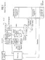
- FIG. 1 shows an addressing device for addressing a data memory according to the prior art.
- a large number of instructions are stored in a program memory, those when executing the program over data lines be loaded into a command register.
- the one in that Command register loaded program command consists of a command opcode, a data storage segment pointer and an offset address.
- the command opcode is used to execute the command in a central control, for example a microprocessor loaded.
- the data storage segment pointer controls one Multiplexer on the input side to several data storage segment registers connected. Depending on that Data storage segment pointer, the multiplexer switches a data storage segment register through at its exit. To this The data content of the connected data storage segment register becomes as higher order address bits in an address register registered, the data content of the switched Data storage segment register that addressed Data storage segment of the data storage indicates.
- the one in the Offset address bits contained in command registers are called low-order address bits copied directly into the address register.
- the physical address is in the address register for addressing a data storage element within the Cached. Thereby the physical Address from the start address of the addressed Data storage segments and the offset address together.
- 2 L data storage segment registers can be selected, so that a maximum of 2 L data storage segments within the data storage can also be addressed if the data content of the data storage segment registers is not modified during the program run.
- the data storage segment pointer comprises two bits, namely the bit positions 14, 15 within the command register and the offset address 14 bits, namely the bit positions 0-13 within the command register.
- the data memory segment pointer can be used to address four different data memory segment registers DPP0 - DPP3. Each of these data storage segment registers has a bit width of 10 bits.
- a physical address with a bit width of 24 bits is formed in the address register, the higher order 10 bits according to Table 1 being written from a data storage segment register and the lower order 14 bits being copied from the offset address of the command register.
- the addressing device shown in Fig. 1 after The prior art has the disadvantage that the number of addressable Data storage segment register as well as the storage size of the individual data storage segments is defined. The addressing is therefore very inflexible. At the above in The example given in the table can use four data storage segment registers be addressed so that on four data storage segments of data storage, each a fixed Memory size of 16 kByte can be accessed can.
- Each data storage segment register has a bit width of 11 bits.
- a physical address with a bit width of 24 bits is formed in the address register, the higher order 11 bits according to Table 2 being written from a data storage segment register and the lower order 13 bits being copied from the offset address of the command register.
- Addressing device gives the memory configuration register field an illustration rule, which for every single bit of the configuration bits stored in the command register specifies whether this is used as an offset address bit or as a selection bit for selecting a data storage segment register / Interpret additional data storage segment register and also specifies which data storage segment registers / Additional data storage segment registers still available for selection stand.
- Addressing device is every bit of the in configuration bits stored in the command register either as a selection bit for selecting a data storage segment register / Additional data storage segment register or as additional offset address bit interpreted.
- Addressing device gives the number from the addressed data storage segment register / additional data storage segment register bits read that the Switch mechanism in the higher order address bits of the address register registers by the calculation rule (h-o), where h the number of high order address bits of the address register and o is the number of additional offset address bits is.
- Addressing device has a switching mechanism that the higher order address bits from the additional offset address bits and the one from the selected data storage segment register / additional data storage segment register bits read together.
- command register there are preferably offset address bits, Configuration bits, selection bits and opcode bits are buffered.
- the number of the higher order address bits is preferably constant.
- the number of least significant address bits is preferably constant.
- the memory size of the addressed data storage segment results from the calculation rule (2 o + z-1 ), where o is the number of offset address bits and z is the number of additional offset address bits.
- the command register 2 shows an addressing device 1 according to the invention with a command register 2, which is connected via data lines 3 is connected to a program memory 4.
- the command register 2 are to be executed via the data lines 3
- the program instruction written in the instruction register 2 comprises an instruction opcode with k data bits that are contained in one first area 2a of the command register can be written.
- the command opcode data bits are sent over lines 5 into one central controller 6, for example a microprocessor, registered that executes the encoded command.
- the central one Control controls the program memory via control lines 7 4 thus the program flow.
- the program command contains in addition to the command opcode bits, a memory configuration selection pointer, which consists of several selection bits, the written in a second area 2b of the command register become.
- the program command contains configuration bits, which are written in a third area 2c of the command register 2 become. It also contains from the program memory 4 read command offset address bits that written in a fourth area 2d of the command register 2 become.
- the area 2d is via data lines 18 with an address register 19 for copying the offset address bits connected.
- Memory configuration selection pointer comprising L selection bits is read in via lines 8 through a switching mechanism 9, that over lines 10 with a memory configuration register 11 is connected.
- the memory configuration register 11 comprises a plurality of memory configuration register fields 11a, 11b ... each memory configuration register field within of the memory configuration register 11 gives a desired one Mapping rule for generating a data storage address of the data storage. Every single bit of the configuration bits 2c becomes dependent on the through the L selection bits selected mapping rule or mapping command by the switching mechanism 9 either as an additional offset address bit or as a selection bit for selecting a data storage segment register / Additional data storage segment register interpreted, being determined by the selected mapping rule is which data storage segment register / additional data storage segment register are still available.
- the switching mechanism 9 is also connected via data lines 12 to the third area 2c of the command register 2 for loading the therein contained configuration bits connected.
- the rear derailleur 9 is via data lines 13 with N data storage segment registers 14 connected.
- the rear derailleur 9 is over Lines 15 on M additional data storage segment registers 16 connected.
- the one in the Memory area 2b of the command register 2 buffered Memory configuration selection pointer of the loaded command is read in by the switching mechanism 9, the data content the one addressed by the memory configuration selection pointer Memory configuration register field 11-i within the Memory configuration register 11 reads. In the memory configuration register field 11-i specifies which data storage segment registers / Additional data storage segment register still available for the generation of the data storage address stand.
- each one Bit of the configuration bits 2c indicates whether this is a selection bit to select a data storage segment register / additional data storage segment register is to be interpreted or as Additional offset address bit is to be interpreted.
- the physical address is in the address register 19 Addressing a data storage element within the data storage cached.
- the address register 19 is divided in higher order address bits 19a and lower order Address bits 19b.
- the address register 19 is via address lines 20 connected to a data memory 21, which via a data bus 22 is connected to the controller 6.
- the switching mechanism 9 is connected via data lines 17 to the higher order ones Address bits 19a of the address register 19 connected.
- The are low-order address bits 19b of the address register 19 connected to the area 2d of the command register.
- the switching mechanism 9 sets the higher order address bits 19a physical cached in the address register 19 Address depending on the one from the memory configuration register field 11-i read the figure together.
- the higher order address bits are generated by the switching mechanism 9 from the additional offset address bits which are dependent from the mapping rule from the configuration bits 2c can be read out, and from the bits that come from the selected one Data storage segment register 14-i / additional data storage segment register 16-i can be read out, put together and via lines 17 into the area 19a of the address register 19 registered.
- the bit width of the fields 19a and 19b of the address register 19 is always constant, as a result of which the bit width of the address register 19 also remains constant.
- the memory size of the addressed data storage segment results from the calculation rule (2 o + z-1 ), where o is the number of offset address bits and z is the number of additional offset address bits.
- Tables 3, 4, 5 and 6 describe a preferred embodiment of the switching mechanism 9 within the invention Addressing device 1.
- the memory configuration selection pointer comprises two bits, namely the bit positions 14, 15 within the command register 2, the configuration bits a single bit, namely bit 13 within the command register 2 and the offset address 13 bits, namely the bit positions 0-12 within the Command register 2.
- the memory configuration register 11 contains four memory configuration register fields, which are referred to as DPP0SEL, DPP1SEL, DPP2SEL, DPP3SEL.
- the switching mechanism 9 reads in via the lines 8 the memory configuration selection pointer, which in the example shown comprises the bits 14-15 within the command register 2.
- the switching mechanism 9 reads out the mapping rule from the addressed memory configuration register field of the memory configuration register 11 in accordance with the memory configuration selection pointer present and, depending on the memory configuration specified there, forms the physical address which is written into the address register 19.
- the contents of the memory configuration register field indicate for every single configuration bit of the command register indicates whether it as a selection bit for selecting a data storage segment register / Additional data storage segment register or as additional offset address bit is to be interpreted and also puts determines which data storage segment registers / additional data storage segment registers are still available.
- bit 13 of the command register in which the configuration bit is stored as Interpreting selection bit or additional offset address bit is. If this bit is interpreted as an additional offset address bit the data storage segment register DPP0 is addressed (see row 3 of table 3), in which case 10 bits read from the data storage segment register DPP0 and together with the additional offset address bit in the 11 high-order bits of the address register can be written.
- Bit 13 of the command register becomes a selection bit interpreted, this bit is used between the data storage segment register DPP0 and the additional data storage segment register EDPP0 selected, and according to the Lines 4 and 5 in Table 3 are addressed 11 bits of the Data storage segment register / additional data storage segment register read out and into the higher order Address register bits written.
- bit 13 of the command register in which the configuration bit is stored as Interpreting selection bit or additional offset address bit is. If this bit is interpreted as an additional offset address bit is addressed, the data storage segment register DPP1 is addressed (see row 3 of table 4), in which case 10 bits are read from the data storage segment register DPP1 and together with the additional offset address bit in the 11 high-order bits of the address register can be written.
- Bit 13 of the command register becomes a selection bit interpreted, this bit is used between the data storage segment register DPP1 and the additional data storage segment register EDPP1 selected, and according to the Lines 4 and 5 in Table 4 are addressed 11 bits of the Data storage segment register / additional data storage segment register read out and into the higher order Address register bits written.
- bit 13 of the command register in which the configuration bit is stored as Interpreting selection bit or additional offset address bit is. If this bit is interpreted as an additional offset address bit is addressed, the data storage segment register DPP1 is addressed (see row 3 of table 5), in which case 10 bits are read from the data storage segment register DPP2 and together with the additional offset address bit in the 11 high-order bits of the address register can be written.
- Bit 13 of the command register becomes a selection bit interpreted, this bit is used between the data storage segment register DPP2 and the additional data storage segment register EDPP2 selected, and according to the Lines 4 and 5 in Table 5 are addressed 11 bits of the Data storage segment register / additional data storage segment register read out and into the higher order Address register bits written.
- the memory configuration register 11 it is possible through the memory configuration register 11 the number of data storage segments within the data storage 21 according to a desired memory configuration to increase and at the same time the runnability of previous to ensure existing programs. By increasing the number of data storage segments it is possible to add new ones Write programs that target many data storage segments access at the same time without the memory requirements of the program go up.
Landscapes
- Engineering & Computer Science (AREA)
- Software Systems (AREA)
- Theoretical Computer Science (AREA)
- Physics & Mathematics (AREA)
- General Engineering & Computer Science (AREA)
- General Physics & Mathematics (AREA)
- Executing Machine-Instructions (AREA)
Abstract
Description
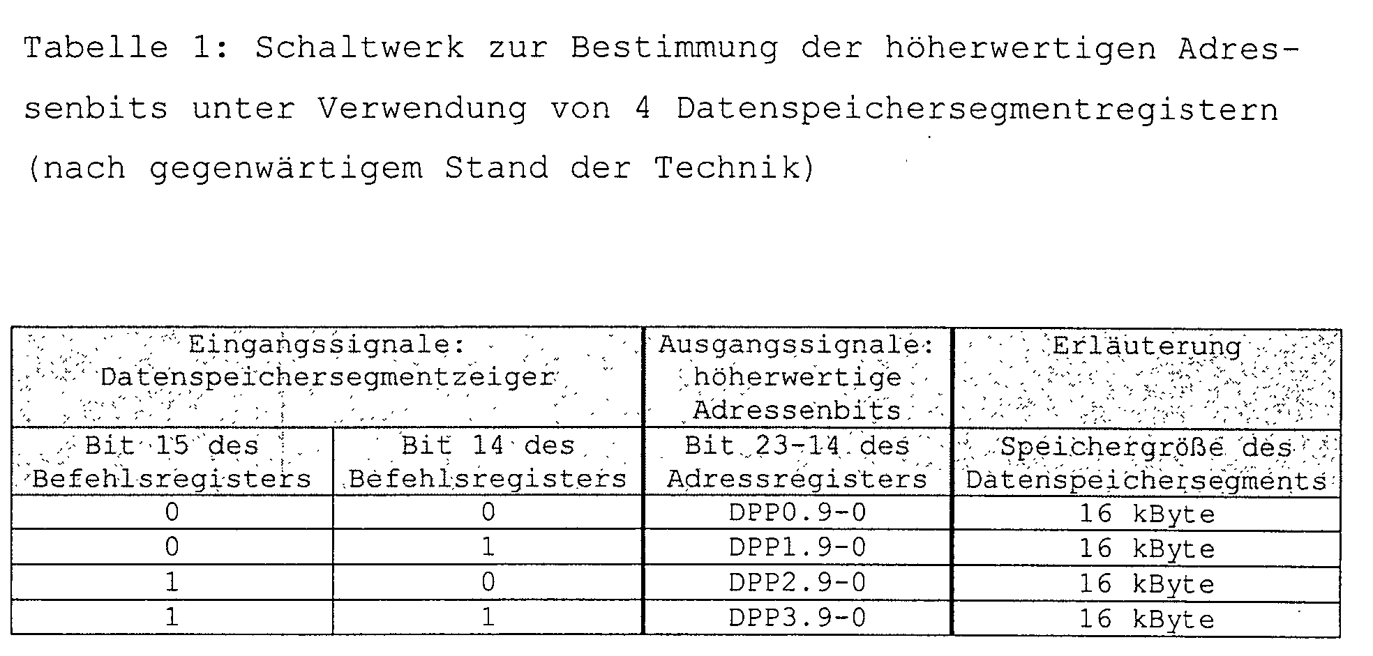
- DPP0.9-0: Bits 9-0 des Datenspeichersegmentregisters DPP0
- DPP1.9-0: Bits 9-0 des Datenspeichersegmentregisters DPP1
- DPP2.9-0: Bits 9-0 des Datenspeichersegmentregisters DPP2
- DPP3.9-0: Bits 9-0 des Datenspeichersegmentregisters DPP3
- 16 kByte = 16 * 1024 Byte = 213 Byte
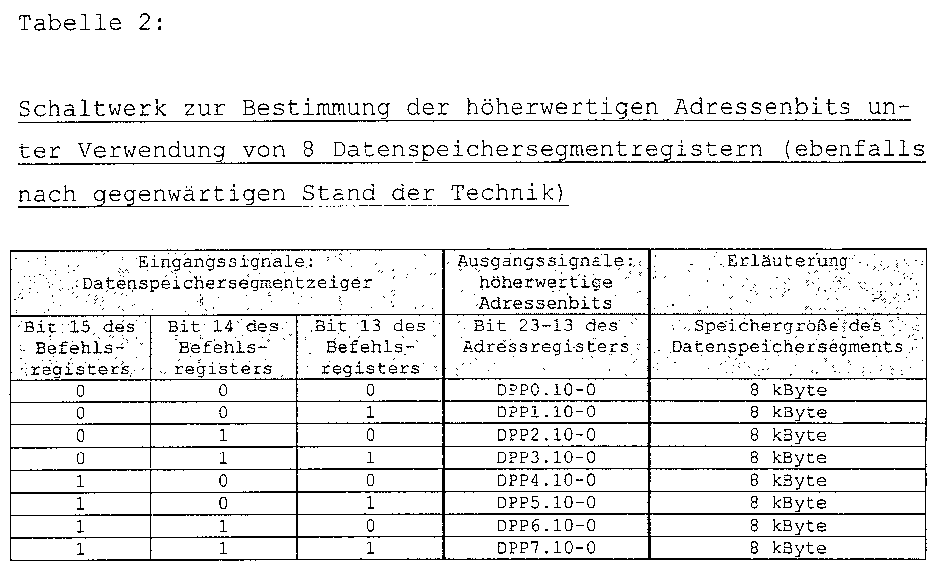
- DPP0.10-0: Bits 10-0 des Datenspeichersegmentregisters DPP0
- DPP1.10-0: Bits 10-0 des Datenspeichersegmentregisters DPP1
- DPP2.10-0: Bits 10-0 des Datenspeichersegmentregisters DPP2
- DPP3.10-0: Bits 10-0 des Datenspeichersegmentregisters DPP3
- DPP4.10-0: Bits 10-0 des Datenspeichersegmentregisters DPP4
- DPP5.10-0: Bits 10-0 des Datenspeichersegmentregisters DPP5
- DPP6.10-0: Bits 10-0 des Datenspeichersegmentregisters DPP6
- DPP7.10-0: Bits 10-0 des Datenspeichersegmentregisters DPP7
- 8 KByte = 8 * 1024 Byte = 212 Byte
- Fig. 1
- eine Adressierungsvorrichtung für einen Datenspeicher nach dem Stand der Technik;
- Fig. 2
- ein Blockschaltbild mit einer erfindungsgemäßen Adressierungsvorrichtung für einen Datenspeicher.
Die Speichergröße des adressierten Datenspeichersegments ergibt sich durch die Berechnungsvorschrift (2o+z-1), wobei o die Anzahl der Offset-Adressenbits ist, und z die Anzahl der Zusatz-Offset-Adressenbits ist.
Das Speicherkonfigurationsregister 11 enthält in dem gezeigten Beispiel vier Speicherkonfigurationsregisterfelder, die als DPP0SEL, DPP1SEL, DPP2SEL, DPP3SEL bezeichnet werden.
In dem gezeigten Beispiel wird das Speicherkonfigurationsregisterfeld DPP0SEL adressiert, wenn Bit 15 des Befehlsregisters = 0 und Bit 14 des Befehlsregisters = 0, und in diesem Fall wird die Abbildungsvorschrift zur Bestimmung der höherwertigen Bits der physikalischen Adresse gemäß Tabelle 3 ausgeführt.
Das Speicherkonfigurationsregisterfeld DPP1SEL wird adressiert, wenn Bit 15 des Befehlsregisters = 0 und Bit 14 des Befehlsregisters = 1, und in diesem Fall wird die Abbildungsvorschrift zur Bestimmung der höherwertigen Bits der physikalischen Adresse gemäß Tabelle 4 ausgeführt.
Das Speicherkonfigurationsregisterfeld DPP2SEL wird adressiert, wenn Bit 15 des Befehlsregisters = 1 und Bit 14 des Befehlsregisters = 0, und in diesem Fall wird die Abbildungsvorschrift zur Bestimmung der höherwertigen Bits der physikalischen Adresse gemäß Tabelle 5 ausgeführt.
Das Speicherkonfigurationsregisterfeld DPP3SEL wird adressiert, wenn Bit 15 des Befehlsregisters = 1 und Bit 14 des Befehlsregisters = 1, und in diesem Fall wird die Abbildungsvorschrift zur Bestimmung der höherwertigen Bits der physikalischen Adresse gemäß Tabelle 6 ausgeführt.

- DPP0.9-0: Bits 9-0 des Datenspeichersegmentregisters DPP0
- DPP0.10: Bit 10 des Datenspeichersegmentregisters DPP0
- EDPP0.9-0: Bits 9-0 des Zusatz-Datenspeichersegmentregisters EDPP0
- EDPP0.10: Bit 10 des Zusatz-Datenspeichersegmentregisters EDPP0


- DPP1.9-0: Bits 9-0 des Datenspeichersegmentregisters DPP1
- DPP1.10: Bit 10 des Datenspeichersegmentregisters DPP1
- EDPP1.9-0: Bits 9-0 des Zusatz-Datenspeichersegmentregisters EDPP1
- EDPP1.10: Bit 10 des Zusatz-Datenspeichersegmentregisters EDPP1

- DPP2.9-0: Bits 9-0 des Datenspeichersegmentregisters DPP2
- DPP2.10: Bit 10 des Datenspeichersegmentregisters DPP2
- EDPP2.9-0: Bits 9-0 des Zusatz-Datenspeichersegmentregisters EDPP2
- EDPP2.10: Bit 10 des Zusatz-Datenspeichersegmentregisters EDPP2

- DPP3.9-0: Bits 9-0 des Datenspeichersegmentregisters DPP3
- DPP3.10: Bit 10 des Datenspeichersegmentregisters DPP3
- EDPP3.9-0: Bits 9-0 des Zusatz-Datenspeichersegmentregisters EDPP3
- EDPP3.10: Bit 10 des Zusatz-Datenspeichersegmentregisters EDPP3
- 1
- Adressierungsvorrichtung
- 2
- Befehlsregister
- 3
- Leitungen
- 4
- Programmspeicher
- 5
- Leitungen
- 6
- Zentrale Steuerung
- 7
- Steuerleitungen
- 8
- Leitungen
- 9
- Schaltwerk
- 10
- Leitungen
- 11
- Speicherkonfigurationsregister
- 12
- Leitungen
- 13
- Leitungen
- 14
- Datenspeichersegmentregister
- 15
- Leitungen
- 16
- Zusatz-Datenspeichersegmentregister
- 17
- Leitungen
- 18
- Leitungen
- 19
- Adressregister
- 20
- Adressenleitungen
- 21
- Datenspeicher
Claims (8)
- Vorrichtung zur Adressierung eines Datenspeichers (21), wobei die Vorrichtung (1) aufweist:wobei die niedrigwertigen Adressenbits des Adressregisters (19) aus den in dem Befehlsregister (2) zwischengespeicherten Offset-Adressenbits (2d) entnommen werden.(a) ein Befehlsregister (2) zum Zwischenspeichern eines Programmbefehls, der
einen Befehls-Opcode (2a), einen Speicherkonfigurationsauswahlzeiger (2b) zur Auswahl eines Speicherkonfigurationsregisterfeldes. Konfigurationsbits (2c) und Offset-Adressenbits (2d) umfasst;(b) ein Speicherkonfigurationsregister (11), das mehrere Speicherkonfigurationsregisterfelder (11-i) umfasst, die verschiedene Abbildungsbefehle zur Generierung einer Datenspeicheradresse des Datenspeichers (21) speichern;(c) mehreren Datenspeichersegmentregistern (14), die jeweils höherwertige Adressenbits einer Anfangsadresse eines Datenspeichersegments speichern, mindestens ein Zusatz-Datenspeichersegmentregister (16), das höherwertige Adressenbits einer Anfangsadresse eines Datenspeichersegments speichert,(d) ein Schaltwerk (9), das in Abhängigkeit von dem aus dem Befehlsregister (2) ausgelesenen Speicherkonfigurationsauswahlzeiger (2b) den Abbildungsbefehl aus dem ausgewählten Speicherkonfigurationsregisterfeld (11-i) ausliest und entsprechend dem ausgelesenen Abbildungsbefehl jedes einzelne Bit der Konfigurationsbits (2c) entweder als Auswahlbit oder als Zusatz-Offset-Adressenbit interpretiert, und die höherwertigen Adressenbits aus dem durch die Auswahlbits selektierten Datenspeichersegmentregister (14) / Zusatz-Datenspeichersegmentregister (16) und aus den Zusatz-Offset-Adressenbits zusammensetzt und in die höherwertigen Bitpositionen eines Adressregisters (19), das eine Datenspeicheradresse zur Adressierung des Datenspeichers (21) zwischenspeichert, einschreibt, - Vorrichtung nach Anspruch 1,
dadurch gekennzeichnet, dass das Speicherkonfigurationsregisterfeld (11-i) eine Abbildungsvorschrift enthält, die für jedes einzelne Bit der Konfigurationsbits (2c) festlegt, ob es als Zusatz-Offset-Adressenbit oder als Auswahlbit zur Auswahl eines Datenspeichersegmentregisters (14) bzw. Zusatz-Datenspeichersegmentregisters (16) zu interpretieren ist, und außerdem angibt, welche Datenspeichersegmentregister (14) bzw. Zusatz-Datenspeichersegmentregister (16) noch zur Auswahl stehen. - Vorrichtung nach einem der vorangehenden Ansprüche,
dadurch gekennzeichnet, dass das Schaltwerk (9) die höherwertigen Adressenbits aus den Zusatz-Offset-Adressenbits, die durch die aus dem Speicherkonfigurationsregisterfeld (11-i) ausgelesenen Abbildungsvorschrift aus den Konfigurationsbits (2c), die aus dem Befehlsregister (2) ausgelesen werden, selektiert werden, und aus dem ausgewähltem Datenspeichersegmentregister (14) / Zusatz-Datenspeichersegmentregister (16) zusammensetzt. - Vorrichtung nach ein dem vorangehenden Ansprüche,
dadurch gekennzeichnet, dass die Zusatz-Offset-Adressenbits durch das Schaltwerk in die höherwertigen Adressenbits des Adressregisters (19) eingeschrieben werden. - Vorrichtung nach ein dem vorangehenden Ansprüche,
dadurch gekennzeichnet, dass sich die Anzahl der aus dem adressierten Datenspeichersegmentregister / Zusatz-Datenspeichersegmentregister ausgelesenen Bits, die das Schaltwerk in die höherwertigen Adressenbits des Adressregisters einschreibt, durch die Berechnungsvorschrift (h-o) ergibt, wobei h die Anzahl der höherwertigen Adressenbits des Adressregisters ist und o die Anzahl der Zusatz-Offset-Adressenbits ist. - Vorrichtung nach ein dem vorangehenden Ansprüche,
dadurch gekennzeichnet, dass in dem Befehlsregister Offset-Adressenbits (2d), Konfigurationsbits (2c), Auswahlbits (2b) und Opcode-Bits (2a) zwischengespeichert sind. - Vorrichtung nach einem der vorangehenden Ansprüche,
dadurch gekennzeichnet, dass das Adressregister (19) mehrere Adressenbits umfasst, wobei die in dem Befehlsregister (2) gespeicherten Offset-Adressenbits (2d) als niederwertige Adressenbits direkt in das Adressregister (19) kopiert werden, und wobei die höherwertigen Adressenbits durch das Schaltwerk (9) in Abhängigkeit von dem Dateninhalt des durch die in dem Befehlsregister gespeicherten Auswahlbits (2b) ausgewählten Speicherkonfigurationsregisterfeldes (11-i) aus einem Datenspeichersegmentregister (14)/ Zusatz-Datenspeichersegmentregister (16) und aus dem in dem Befehlsregister (2) gespeicherten Konfigurationsbits (2c) eingeschrieben werden. - Vorrichtung nach ein dem vorangehenden Ansprüche,
dadurch gekennzeichnet, dass die Anzahl der höherwertigen Adressenbits (19a) und die Anzahl der niedrigwertigen Adressenbits (19b) konstant ist.
Applications Claiming Priority (2)
| Application Number | Priority Date | Filing Date | Title |
|---|---|---|---|
| DE10131124 | 2001-06-28 | ||
| DE10131124A DE10131124A1 (de) | 2001-06-28 | 2001-06-28 | Konfigurierbare Adressierungsvorrichtung |
Publications (2)
| Publication Number | Publication Date |
|---|---|
| EP1271306A2 true EP1271306A2 (de) | 2003-01-02 |
| EP1271306A3 EP1271306A3 (de) | 2007-07-25 |
Family
ID=7689725
Family Applications (1)
| Application Number | Title | Priority Date | Filing Date |
|---|---|---|---|
| EP02014434A Withdrawn EP1271306A3 (de) | 2001-06-28 | 2002-06-28 | Konfigurierbare Adressierungsvorrichtung |
Country Status (3)
| Country | Link |
|---|---|
| US (1) | US20030126397A1 (de) |
| EP (1) | EP1271306A3 (de) |
| DE (1) | DE10131124A1 (de) |
Cited By (1)
| Publication number | Priority date | Publication date | Assignee | Title |
|---|---|---|---|---|
| CN111124311A (zh) * | 2019-12-23 | 2020-05-08 | 四川效率源信息安全技术股份有限公司 | 一种逻辑卷管理下基于配置信息的raid数据的恢复方法 |
Families Citing this family (3)
| Publication number | Priority date | Publication date | Assignee | Title |
|---|---|---|---|---|
| WO2015173853A1 (ja) * | 2014-05-12 | 2015-11-19 | 株式会社日立製作所 | 情報処理装置、その処理方法、及び入出力装置 |
| CN105224346B (zh) * | 2014-05-28 | 2019-11-29 | 腾讯科技(深圳)有限公司 | 目标函数定位方法及装置 |
| JP2020071888A (ja) * | 2018-10-29 | 2020-05-07 | キオクシア株式会社 | 記憶装置及び記憶方法 |
Family Cites Families (6)
| Publication number | Priority date | Publication date | Assignee | Title |
|---|---|---|---|---|
| JPS6017130B2 (ja) * | 1980-06-06 | 1985-05-01 | 日本電気株式会社 | アドレス制御装置 |
| US4453212A (en) * | 1981-07-13 | 1984-06-05 | Burroughs Corporation | Extended address generating apparatus and method |
| US5386523A (en) * | 1992-01-10 | 1995-01-31 | Digital Equipment Corporation | Addressing scheme for accessing a portion of a large memory space |
| US5918251A (en) * | 1996-12-23 | 1999-06-29 | Intel Corporation | Method and apparatus for preloading different default address translation attributes |
| US6088780A (en) * | 1997-03-31 | 2000-07-11 | Institute For The Development Of Emerging Architecture, L.L.C. | Page table walker that uses at least one of a default page size and a page size selected for a virtual address space to position a sliding field in a virtual address |
| US6349380B1 (en) * | 1999-03-12 | 2002-02-19 | Intel Corporation | Linear address extension and mapping to physical memory using 4 and 8 byte page table entries in a 32-bit microprocessor |
-
2001
- 2001-06-28 DE DE10131124A patent/DE10131124A1/de not_active Withdrawn
-
2002
- 2002-06-27 US US10/185,848 patent/US20030126397A1/en not_active Abandoned
- 2002-06-28 EP EP02014434A patent/EP1271306A3/de not_active Withdrawn
Cited By (2)
| Publication number | Priority date | Publication date | Assignee | Title |
|---|---|---|---|---|
| CN111124311A (zh) * | 2019-12-23 | 2020-05-08 | 四川效率源信息安全技术股份有限公司 | 一种逻辑卷管理下基于配置信息的raid数据的恢复方法 |
| CN111124311B (zh) * | 2019-12-23 | 2023-06-23 | 四川效率源信息安全技术股份有限公司 | 一种逻辑卷管理下基于配置信息的raid数据的恢复方法 |
Also Published As
| Publication number | Publication date |
|---|---|
| US20030126397A1 (en) | 2003-07-03 |
| EP1271306A3 (de) | 2007-07-25 |
| DE10131124A1 (de) | 2003-01-23 |
Similar Documents
| Publication | Publication Date | Title |
|---|---|---|
| DE3588009T2 (de) | Vorrichtung und Verfahren zum Rekonfigurieren eines Speichers in einer Datenverarbeitungsanordnung. | |
| DE2459006C2 (de) | Einrichtung zum Bilden einer absoluten Adresse in einer Datenverarbeitunsanlage | |
| DE69929936T2 (de) | Verfahren und Vorrichtung zum Abrufen von nicht-angrenzenden Befehlen in einem Datenverarbeitungssystem | |
| DE3688824T2 (de) | Datenverarbeitungssystem. | |
| DE3786660T2 (de) | Computersystem mit einer CPU mit zwei gegenseitig inkompatiblen Adressiermoden. | |
| DE69428303T2 (de) | Verfahren und Vorrichtung zum Datenarbeiten mit mehreren Statusbitgruppen | |
| DE69622663T2 (de) | Zweistufige vorausholungspufferstruktur und verfahren mit bypass | |
| EP0097725B1 (de) | Einrichtung im Befehlswerk eines mikroprogrammgesteuerten Prozessors zur direkten hardwaregesteuerten Ausführung bestimmter Instruktionen | |
| DE3486085T2 (de) | Zentrale Verarbeitungseinheit für einen Digitalrechner. | |
| DE69624158T2 (de) | Superskalarer Prozessor mit mehreren Registerblöcken und Erzeugung von spekulativen Antwortadressen | |
| DE69623146T2 (de) | Verfahren und Vorrichtung zum Koordinieren der Benutzung von physikalischen Registern in einem Mikroprozessor | |
| DE2417795C2 (de) | Datenverarbeitungsanlage | |
| DE2360303A1 (de) | Datenverarbeitungssystem mit dynamischer adressuebersetzung | |
| DE2718110A1 (de) | Datenverarbeitungseinheit | |
| DE3856139T2 (de) | Mikroprozessor | |
| DE69231237T2 (de) | Datenverarbeitungsvorrichtung | |
| DE2426874A1 (de) | Verfahren und schaltungsanordnung zur bestimmung der adressenart eines befehls | |
| DE2744359C2 (de) | ||
| DE3116385C2 (de) | Mikroprogramm-Steuerung | |
| DE3650006T2 (de) | Verfahren und Mittel zum Transportieren von Bytes in einem Rechner mit reduziertem Befehlssatz. | |
| DE69807412T2 (de) | Prozessorarchitekturschema und Befehlssatz zur Maximierung verfügbarer Opcodes und zum Einsetzen verschiedener Adressierungsmodi | |
| DE68925376T2 (de) | In Direktabbildung und in Bankabbildung wirksamer Informationsprozessor und Verfahren zum Schalten der Abbildungsschemas | |
| EP1079307B1 (de) | Verfahren zum Betrieb eines Speichersystems sowie Speichersystem | |
| DE69503010T2 (de) | Mikroprozessor zur Ausführung von Befehlen,von denen ein Teil des Operandfelds als Operationscode zu gebrauchen ist | |
| DE3121046A1 (de) | Arithmetik-logikeinheit mit bit-manipulation |
Legal Events
| Date | Code | Title | Description |
|---|---|---|---|
| PUAI | Public reference made under article 153(3) epc to a published international application that has entered the european phase |
Free format text: ORIGINAL CODE: 0009012 |
|
| AK | Designated contracting states |
Kind code of ref document: A2 Designated state(s): AT BE CH CY DE DK ES FI FR GB GR IE IT LI LU MC NL PT SE TR |
|
| AX | Request for extension of the european patent |
Free format text: AL;LT;LV;MK;RO;SI |
|
| PUAL | Search report despatched |
Free format text: ORIGINAL CODE: 0009013 |
|
| AK | Designated contracting states |
Kind code of ref document: A3 Designated state(s): AT BE CH CY DE DK ES FI FR GB GR IE IT LI LU MC NL PT SE TR |
|
| AX | Request for extension of the european patent |
Extension state: AL LT LV MK RO SI |
|
| AKX | Designation fees paid | ||
| STAA | Information on the status of an ep patent application or granted ep patent |
Free format text: STATUS: THE APPLICATION IS DEEMED TO BE WITHDRAWN |
|
| 18D | Application deemed to be withdrawn |
Effective date: 20080126 |
|
| REG | Reference to a national code |
Ref country code: DE Ref legal event code: 8566 |