EP1269543B1 - Cellule active avec memoire analogique pour un capteur photosensible realise en technologie cmos - Google Patents
Cellule active avec memoire analogique pour un capteur photosensible realise en technologie cmos Download PDFInfo
- Publication number
- EP1269543B1 EP1269543B1 EP01919428A EP01919428A EP1269543B1 EP 1269543 B1 EP1269543 B1 EP 1269543B1 EP 01919428 A EP01919428 A EP 01919428A EP 01919428 A EP01919428 A EP 01919428A EP 1269543 B1 EP1269543 B1 EP 1269543B1
- Authority
- EP
- European Patent Office
- Prior art keywords
- cell
- type
- addressable
- photosensitive element
- conductivity type
- Prior art date
- Legal status (The legal status is an assumption and is not a legal conclusion. Google has not performed a legal analysis and makes no representation as to the accuracy of the status listed.)
- Expired - Lifetime
Links
Images

Classifications
-
- H—ELECTRICITY
- H10—SEMICONDUCTOR DEVICES; ELECTRIC SOLID-STATE DEVICES NOT OTHERWISE PROVIDED FOR
- H10F—INORGANIC SEMICONDUCTOR DEVICES SENSITIVE TO INFRARED RADIATION, LIGHT, ELECTROMAGNETIC RADIATION OF SHORTER WAVELENGTH OR CORPUSCULAR RADIATION
- H10F39/00—Integrated devices, or assemblies of multiple devices, comprising at least one element covered by group H10F30/00, e.g. radiation detectors comprising photodiode arrays
- H10F39/80—Constructional details of image sensors
- H10F39/803—Pixels having integrated switching, control, storage or amplification elements
Definitions
- Such a cell has a shutter function which makes it possible to cancel momentarily the influence of the incident light during the waiting time elapsing between the exposure phase and the moment when the cell is read in the addressing order of the network in which it is incorporated.
- the luminance signal detected during the exposure phase is integrated into the memory means which can be implemented as a capacity that is part of the cell.
- the luminance signal being in this type of CMOS cell of analog nature, it is important that the capacity thus used can keep the charge corresponding to this signal without distortion or loss during the entire waiting time until the reading of the cell. Therefore, during this time, the capacity should be isolated as far as possible from the rest of the cell to prevent any leakage of its charge.
- the storage means implemented in the form of a capacity are decoupled from the photosensitive element by the third addressable means at the end of the exposure phase.
- the invention aims to provide an alternative solution to this problem which allows after the exposure phase to isolate almost entirely the accumulation node of loads from the rest of the circuit without greatly increasing the bulk of the cell and reducing almost nothing parasite accumulation.
- An advantage resulting from the invention lies in that the spectral characteristics of the photosensitive element are not altered.
- the charge carriers which, when illuminating the cell would tend to migrate to memory means are stopped at the junction between the substrate and the box in which said third means are placed addressable. They cannot reach the node on which the charges accumulate representing the useful luminance signal.
- the cells shown in the figures are intended to be part of a photosensitive sensor produced using CMOS technology on a semiconductor substrate.
- This substrate comprises a matrix of a large number of cells addressable organized in a manner known per se, for example according to the scheme of the Figure 1 of the above article.
- the matrix undergoes successive cycles of observation of a scene for example, each cycle comprising a phase of exposure of the sensor to the light returned by the scene, followed by an exploitation or acquisition phase during which the cells of the sensor are read in sequence by matrix addressing. So the matrix can deliver a succession of row signals each composed of a variable voltage divided into samples each representing the luminance signal of a cell in the row concerned.
- a cell according to the invention comprises a photosensitive diode 1 connected in series with an n-type transistor 2 which constitutes the first addressable means of the cell and whose gate is connected to receive a deactivation signal from photodiode 1 from a control terminal 3.
- Diode 1 and transistor 2 are connected between ground and a supply voltage (V ss ) of the diode applied to a terminal power supply 4.
- the node 5 between the diode 1 and the transistor 2 is connected to a shutter transistor 6 which materializes the third addressable means of the cell.
- the gate of this transistor 6 is connected to a shutter control terminal 7 of the cell. When it is conductive, this shutter transistor transfers, to the charge accumulation node 8, a signal corresponding to the quantity of charges appearing on the node 5.
- the charge accumulation node 8 is connected to the gate of a transistor 9 acting as a buffer and amplifier, this transistor 9 being mounted so as to be able to convert the useful luminance signal generated by the diode 1 and appearing under form of a voltage on node 8 in a current which can be evacuated from the cell during the reading phase.
- the transistor 9 is connected in series with a read control transistor 10 between a power supply terminal (V DD ) 11 and an output line 12 which in the cell matrix is a column line.
- the gate of transistor 10 is connected to a read control terminal 13.
- Transistors 9 and 10 materialize the second addressable means of the cell.
- Node 8 is connected to several parasitic capacities cp1, cp2 and cp3.
- the capacity cp1 which is the most important is located between node 8 and ground, while the- two other capacities cp2 and cp3 connect the node 8 on either side of the transistor 9.
- these stray capacitances materialize the memory resources of the cell, their total value generally being sufficient for the conservation of the charge after the exposure phase until the cell is read. Yes this was not the case in a given implementation, we could consider integrating with the cell circuit a capacity suitably sized and connected by example between node 8 and ground.
- the node 8 is also connected to a reset transistor 14 (fourth means) which is intended to keep the node 8 discharged between each reading and the next exposure phase of the cell.
- This transistor 14 is controlled for this purpose by a signal applied to a terminal 15 connected to its gate.
- the drain-source path of this transistor 14 is connected between the node 8 and the terminal V DD .
- the implementation of the cell in Figure 1 is partially shown and schematically in Figure 2.
- the cell is integrated on a p-type substrate 16 with a plurality of other cells (not shown), all identical, in a matrix which also includes all the addressing and power connections, for example example according to the diagram in FIG. 4 of the aforementioned article.
- the diode 1 is constituted by an n + region 17 produced in the substrate and which is placed behind an opening 18 of a screen 19 intended to reduce the release of charge carriers in the other components of the cell by light incident.
- This screen 19 may be a final layer deposited over all of the cells and having an opening 18 opposite each region 17.
- the photosensitive element 1 is a region capable of collecting the electrons generated by light and which can be an n + or n - doped zone or even a "photogate".
- the shutter transistor 6 and the reset transistor 14 are placed in a box 20 of a conductivity type opposite to that of the substrate 16.
- the two transistors 6 and 14 can share the same box or be made in two separate boxes but with the same type of conductivity.
- this type of conductivity is n.
- the box 20 are formed two diffusion regions p + 21 and 22 of the same type of conductivity as that of the substrate which form, with a gate 23 provided between them, the shutter transistor 6 (the transistor 14 is not shown in Figure 2).
- the box 20 is symbolized by a conductor bearing the same reference as in FIG. 2.
- the diffusion regions 21 and 22 are of the p + type and the diffusion region 24 is of the n + type.
- the transistor 14 is of the p type. It can be produced in the box 20 or in another box, in the example having to be of type n provided elsewhere in the substrate 16. It will also be noted that the node 5 is connected to the transistor 6 by means of a connection 27 external to the substrate 16.
- the time during which the payloads remain stored on the node 8 essentially depends on the leakage current flowing in the diode formed between the p + region 22 and the n-type well 20, a diode whose characteristics depend on the technology used.
- an advantageous characteristic of the invention consists in providing the possibility of biasing at the choice of the designer, the box 20 via the connection 25 and the terminal 26 so as to be able to adjust as best as possible, by adjusting the bias voltage, the charge retention time before a cell reading must be taken.
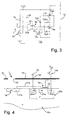
- FIG. 3 and 4 show an embodiment according to a dual form of that of FIG. 1 as regards the types of conductivity used.
- components with the same function but with a conductivity type opposite to that which they have in Figures 1 and 2 have been designated by the same reference with the suffix "a".
- transistors 9 and 10 or 9a, 10a can also be implemented by equivalent means located outside of the chip in which the matrix composed of the cells according to the invention is produced. In this case, of course, the corresponding transistors are not provided in the cell itself.
- the structure of the cell according to the invention also offers the possibility to postpone reading until considered appropriate by the designer by playing in particular on the voltage of the box 20 or 20a.
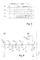
- FIG. 5 shows a diagram of the control signals of the cell of the Figure 1.
- the control signal of transistor 2 is shown in (a); he determines the time exposure.
- In (b) is shown the control signal of the shutter transistor 6.
- the control signal of the reset transistor 14 is shown in (c), while in (d) appears the succession of values read on the different cells (or "pixels") of the sensor.
- Figure 6 shows yet another embodiment of the cell according to the invention.
- the shutter transistor 6 consists in fact of a plurality of transistors (6.1 to 6.3), each being associated with storage means (C1 to C3) and being controlled by a voltage applied to their grid (7.1 to 7.3).
Landscapes
- Solid State Image Pick-Up Elements (AREA)
- Transforming Light Signals Into Electric Signals (AREA)
- Facsimile Heads (AREA)
Description
- un élément photosensible,
- des premiers moyens adressables pour activer/désactiver cet élément photosensible après ladite phase d'exposition,
- des deuxièmes moyens adressables pour, au cours de ladite phase d'exploration, extraire de la cellule le signal de luminance engendrée par ledit élément photosensible,
- des troisièmes moyens adressables pour transférer ledit signal de luminance dudit élément photosensible auxdits deuxièmes moyens adressables;
- des moyens de mémoire pour conserver ledit signal de luminance entre la phase d'exposition et l'instant où ladite cellule est adressée pour l'activation desdits deuxièmes moyens adressables; et
- des quatrièmes moyens adressables pour décharger lesdits moyens de mémoire après la phase de lecture de la cellule, ledit élément photosensible et lesdits premiers, deuxièmes et troisièmes moyens adressables étant implémentés sous la forme de composants semi-conducteurs intégrés dans un substrat avec des types de conductivité prédéterminés.
- ledit premier type de conductivité est le type p et le second type de conductivité est le type n;
- ledit premier type de conductivité est le type n et le second type de conductivité est le type p;
- une région de diffusion est implantée dans ledit caisson et connectée à une source de tension de polarisation de préférence réglable, cette région ayant le second type de conductivité;
- lesdits quatrièmes moyens adressables sont implantés dans ledit caisson;
- lesdits troisièmes moyens consistent en une pluralité de transistors connectés en série et commandés, chacun, par une tension fixe.
- la figure 1 est un schéma d'une cellule pour capteur photosensible selon l'invention, réalisée avec une technologie à substrat p;
- la figure 2 montre schématiquement un exemple d'implémentation d'une cellule représentée sur la figure 1;
- la figure 3 est un schéma d'une cellule selon l'invention réalisée avec une technologie à substrat n;
- la figure 4 est un exemple d'implémentation de la cellule de la figure 3;
- la figure 5 est un diagramme des signaux de la cellule de la figure 3; et
- la figure 6 est encore un autre exemple de réalisation d'une cellule selon l'invention.
Claims (6)
- Cellule active pour un capteur photosensible réalisé en technologie CMOS et comprenant une pluralité de ces cellules agencées selon une matrice adressable dans laquelle les cellules subissent des cycles de travail successifs consistant, au moins, en une phase d'exposition pour détecter la quantité de lumière qui les frappe, puis en une phase d'exploration au cours de laquelle l'information de luminance due à cette quantité de lumière est extraite de la cellule, cette cellule comprenantun élément photosensible (1),des premiers moyens adressables (2) pour activer/désactiver cet élément photosensible après ladite phase d'exposition,des deuxièmes moyens adressables (9, 10) pour, au cours de ladite phase d'exploration, extraire de la cellule le signal de luminance engendré par ledit élément photosensible (1),des troisièmes moyens adressables (6) pour transférer ledit signal de luminance dudit élément photosensible (1) auxdits deuxièmes moyens adressables (8, 10);des moyens de mémoire (cp1 à cp3) pour conserver ledit signal de luminance entre la phase d'exposition et l'instant où ladite cellule est adressée pour l'activation desdits deuxièmes moyens adressables (9, 10), etdes quatrièmes moyens adressables pour décharger lesdits moyens de mémoire après la phase de lecture de la cellule, ledit élément photosensible et lesdits premiers, seconds, troisièmes et quatrièmes moyens adressables étant implémentés sous la forme de composants semi-conducteurs intégrés dans un substrat (16) avec des types de conductivité prédéterminés, lesdits troisièmes et quatrièmes moyens adressables étant placés dans au moins un caisson (20) ménagé dans le substrat (16), ledit au moins un caisson présentant un premier type de conductivité opposé à celui du substrat, qui présente un second type de conductivité et dans lequel est réalisé l'élément photosensible (1).
- Cellule suivant la revendication 1, caractérisée en ce que ledit premier type de conductivité est le type p et le second type de conductivité est le type n.
- Cellule suivant la revendication 1, caractérisée en ce que ledit premier type de conductivité est le type n et le second type de conductivité est le type p.
- Cellule suivant l'une quelconque des revendications précédentes, caractérisée en ce qu'une région de diffusion (24) est implantée dans ledit caisson (20) et connectée à une source de tension de polarisation (26), de préférence réglable, cette région ayant le second type de conductivité.
- Cellule suivant la revendication 4, caractérisée en ce que lesdits quatrièmes moyens adressables (14) sont implantés dans ledit caisson (20).
- Cellule selon l'une quelconque des revendications 1 à 5, caractérisée en ce que lesdits troisièmes moyens consistent en une pluralité de transistors (6.1 à 6.3) connectés en série et commandés, chacun, par une tension fixe.
Applications Claiming Priority (3)
| Application Number | Priority Date | Filing Date | Title |
|---|---|---|---|
| FR0004494 | 2000-04-07 | ||
| FR0004494A FR2807570B1 (fr) | 2000-04-07 | 2000-04-07 | Cellule active avec memoire analogique pour un capteur photosensible realise en technologie cmos |
| PCT/EP2001/003841 WO2001078150A1 (fr) | 2000-04-07 | 2001-04-04 | Cellule active avec memoire analogique pour un capteur photosensible realise en technologie cmos |
Publications (2)
| Publication Number | Publication Date |
|---|---|
| EP1269543A1 EP1269543A1 (fr) | 2003-01-02 |
| EP1269543B1 true EP1269543B1 (fr) | 2004-10-13 |
Family
ID=8849014
Family Applications (1)
| Application Number | Title | Priority Date | Filing Date |
|---|---|---|---|
| EP01919428A Expired - Lifetime EP1269543B1 (fr) | 2000-04-07 | 2001-04-04 | Cellule active avec memoire analogique pour un capteur photosensible realise en technologie cmos |
Country Status (6)
| Country | Link |
|---|---|
| US (1) | US6838652B2 (fr) |
| EP (1) | EP1269543B1 (fr) |
| AT (1) | ATE279788T1 (fr) |
| DE (1) | DE60106412T2 (fr) |
| FR (1) | FR2807570B1 (fr) |
| WO (1) | WO2001078150A1 (fr) |
Families Citing this family (4)
| Publication number | Priority date | Publication date | Assignee | Title |
|---|---|---|---|---|
| CA2301345A1 (fr) * | 2000-03-17 | 2001-09-17 | Semiconductor Insights Inc. | Prise de cliche |
| WO2002063691A2 (fr) * | 2001-02-02 | 2002-08-15 | Symagery Microsystems Inc. | Cellule de pixel actif avec condensateur |
| JP2006505159A (ja) * | 2002-10-29 | 2006-02-09 | フォトンフォーカス アクチェンゲゼルシャフト | 光電センサ |
| DE602005006570D1 (de) * | 2004-07-28 | 2008-06-19 | Iee Sarl | Nachweis und analyse optischer sensorsonden |
Family Cites Families (8)
| Publication number | Priority date | Publication date | Assignee | Title |
|---|---|---|---|---|
| DE4209536C3 (de) * | 1992-03-24 | 2000-10-05 | Stuttgart Mikroelektronik | Bildzelle für einen Bildaufnehmer-Chip |
| US5471515A (en) * | 1994-01-28 | 1995-11-28 | California Institute Of Technology | Active pixel sensor with intra-pixel charge transfer |
| US6297070B1 (en) * | 1996-12-20 | 2001-10-02 | Eastman Kodak Company | Active pixel sensor integrated with a pinned photodiode |
| JP3695933B2 (ja) * | 1997-03-18 | 2005-09-14 | 株式会社東芝 | 固体撮像装置 |
| TW421962B (en) * | 1997-09-29 | 2001-02-11 | Canon Kk | Image sensing device using mos type image sensing elements |
| US6369853B1 (en) * | 1997-11-13 | 2002-04-09 | Foveon, Inc. | Intra-pixel frame storage element, array, and electronic shutter method suitable for electronic still camera applications |
| US6069376A (en) * | 1998-03-26 | 2000-05-30 | Foveonics, Inc. | Intra-pixel frame storage element, array, and electronic shutter method including speed switch suitable for electronic still camera applications |
| US6512544B1 (en) * | 1998-06-17 | 2003-01-28 | Foveon, Inc. | Storage pixel sensor and array with compression |
-
2000
- 2000-04-07 FR FR0004494A patent/FR2807570B1/fr not_active Expired - Fee Related
-
2001
- 2001-04-04 AT AT01919428T patent/ATE279788T1/de not_active IP Right Cessation
- 2001-04-04 WO PCT/EP2001/003841 patent/WO2001078150A1/fr not_active Ceased
- 2001-04-04 EP EP01919428A patent/EP1269543B1/fr not_active Expired - Lifetime
- 2001-04-04 DE DE60106412T patent/DE60106412T2/de not_active Expired - Fee Related
-
2002
- 2002-10-04 US US10/264,711 patent/US6838652B2/en not_active Expired - Fee Related
Also Published As
| Publication number | Publication date |
|---|---|
| FR2807570A1 (fr) | 2001-10-12 |
| US6838652B2 (en) | 2005-01-04 |
| US20030062549A1 (en) | 2003-04-03 |
| WO2001078150A1 (fr) | 2001-10-18 |
| DE60106412T2 (de) | 2006-02-23 |
| EP1269543A1 (fr) | 2003-01-02 |
| FR2807570B1 (fr) | 2003-08-15 |
| ATE279788T1 (de) | 2004-10-15 |
| DE60106412D1 (de) | 2004-11-18 |
Similar Documents
| Publication | Publication Date | Title |
|---|---|---|
| EP3188238B1 (fr) | Pixel de détection de temps de vol | |
| EP2216817B1 (fr) | Capteur d'images à semiconducteur à éclairement par la face arrière | |
| EP0367650B1 (fr) | Dispositif photosensible du type à amplification du signal au niveau des points photosensibles | |
| FR2775541A1 (fr) | Detecteur d'images cmos, photodiode pour un detecteur de ce type, et procedes pour la fabrication de ce detecteur et de cette photodiode | |
| EP1265291A1 (fr) | Capteur d'image CMOS et procédé permettant d'opérer un capteur d'image CMOS avec une dynamique accrue | |
| EP2912690A1 (fr) | Structure d'un pixel actif de type cmos | |
| EP0474550B1 (fr) | Détecteur d'images à pixels de grandes dimensions | |
| FR3065320A1 (fr) | Pixel de detection de temps de vol | |
| EP0435773B1 (fr) | Dispositif pour prises de vues à circuits de balayage intégrés | |
| EP3629573B1 (fr) | Capteur d'images rapide a regroupement de pixels | |
| FR3089086A1 (fr) | Dispositif imageur intégré avec une capacité de stockage des charges améliorée | |
| EP0331546B1 (fr) | Matrice photosensible à deux diodes par point, sans conducteur spécifique de remise à niveau | |
| WO2008034677A1 (fr) | Capteur d'image lineaire cmos a fonctionnement de type transfert de charges | |
| EP3308399B1 (fr) | Capteur d'image a haute dynamique, a noeud de stockage en trois parties | |
| FR3008826A1 (fr) | Cellule de capteur d'image a gain de conversion double | |
| EP0276594B1 (fr) | Dispositif anti-éblouissement pour capteur d'images à transfert de charges, et capteur d'images comportant un tel dispositif | |
| FR3022425A1 (fr) | Structure de circuit de lecture a injection de charge | |
| WO2001078150A1 (fr) | Cellule active avec memoire analogique pour un capteur photosensible realise en technologie cmos | |
| FR2513015A1 (fr) | Dispositif de detection d'image en couleurs du type transfert de charge | |
| FR2557372A1 (fr) | Procede d'ebasage d'un dispositif photosensible a l'etat solide | |
| FR2857158A1 (fr) | Procede de commande d'un photocopieur de type mos | |
| WO2009068526A1 (fr) | Capteur d'image a pixel a quatre ou cinq transistors avec reduction de bruit de reinitialisation | |
| FR3111014A1 (fr) | Capteur d’image matriciel à sensibilité élevée | |
| EP2177886B1 (fr) | Procédé et dispositif de lecture de charges électriques produites par un photodétecteur, et détecteur comportant de tels dispositifs | |
| FR2966678A1 (fr) | Dispositif d'imagerie en particulier du type cmos a report et integration. |
Legal Events
| Date | Code | Title | Description |
|---|---|---|---|
| PUAI | Public reference made under article 153(3) epc to a published international application that has entered the european phase |
Free format text: ORIGINAL CODE: 0009012 |
|
| 17P | Request for examination filed |
Effective date: 20021023 |
|
| AK | Designated contracting states |
Kind code of ref document: A1 Designated state(s): AT BE CH CY DE DK ES FI FR GB GR IE IT LI LU MC NL PT SE TR |
|
| RAP1 | Party data changed (applicant data changed or rights of an application transferred) |
Owner name: CSEMCENTRE SUISSE D'ELECTRONIQUE ET DEMICROTECHNIQ |
|
| GRAP | Despatch of communication of intention to grant a patent |
Free format text: ORIGINAL CODE: EPIDOSNIGR1 |
|
| GRAS | Grant fee paid |
Free format text: ORIGINAL CODE: EPIDOSNIGR3 |
|
| GRAA | (expected) grant |
Free format text: ORIGINAL CODE: 0009210 |
|
| RIC1 | Information provided on ipc code assigned before grant |
Ipc: 7H 01L 27/146 A Ipc: 7H 04N 3/15 B |
|
| AK | Designated contracting states |
Kind code of ref document: B1 Designated state(s): AT BE CH CY DE DK ES FI FR GB GR IE IT LI LU MC NL PT SE TR |
|
| PG25 | Lapsed in a contracting state [announced via postgrant information from national office to epo] |
Ref country code: IT Free format text: LAPSE BECAUSE OF FAILURE TO SUBMIT A TRANSLATION OF THE DESCRIPTION OR TO PAY THE FEE WITHIN THE PRESCRIBED TIME-LIMIT;WARNING: LAPSES OF ITALIAN PATENTS WITH EFFECTIVE DATE BEFORE 2007 MAY HAVE OCCURRED AT ANY TIME BEFORE 2007. THE CORRECT EFFECTIVE DATE MAY BE DIFFERENT FROM THE ONE RECORDED. Effective date: 20041013 Ref country code: NL Free format text: LAPSE BECAUSE OF FAILURE TO SUBMIT A TRANSLATION OF THE DESCRIPTION OR TO PAY THE FEE WITHIN THE PRESCRIBED TIME-LIMIT Effective date: 20041013 Ref country code: FI Free format text: LAPSE BECAUSE OF FAILURE TO SUBMIT A TRANSLATION OF THE DESCRIPTION OR TO PAY THE FEE WITHIN THE PRESCRIBED TIME-LIMIT Effective date: 20041013 Ref country code: AT Free format text: LAPSE BECAUSE OF FAILURE TO SUBMIT A TRANSLATION OF THE DESCRIPTION OR TO PAY THE FEE WITHIN THE PRESCRIBED TIME-LIMIT Effective date: 20041013 Ref country code: TR Free format text: LAPSE BECAUSE OF FAILURE TO SUBMIT A TRANSLATION OF THE DESCRIPTION OR TO PAY THE FEE WITHIN THE PRESCRIBED TIME-LIMIT Effective date: 20041013 Ref country code: IE Free format text: LAPSE BECAUSE OF FAILURE TO SUBMIT A TRANSLATION OF THE DESCRIPTION OR TO PAY THE FEE WITHIN THE PRESCRIBED TIME-LIMIT Effective date: 20041013 |
|
| REG | Reference to a national code |
Ref country code: GB Ref legal event code: FG4D Free format text: NOT ENGLISH |
|
| REG | Reference to a national code |
Ref country code: CH Ref legal event code: EP |
|
| REG | Reference to a national code |
Ref country code: IE Ref legal event code: FG4D Free format text: FRENCH |
|
| REF | Corresponds to: |
Ref document number: 60106412 Country of ref document: DE Date of ref document: 20041118 Kind code of ref document: P |
|
| PG25 | Lapsed in a contracting state [announced via postgrant information from national office to epo] |
Ref country code: DK Free format text: LAPSE BECAUSE OF FAILURE TO SUBMIT A TRANSLATION OF THE DESCRIPTION OR TO PAY THE FEE WITHIN THE PRESCRIBED TIME-LIMIT Effective date: 20050113 Ref country code: SE Free format text: LAPSE BECAUSE OF FAILURE TO SUBMIT A TRANSLATION OF THE DESCRIPTION OR TO PAY THE FEE WITHIN THE PRESCRIBED TIME-LIMIT Effective date: 20050113 Ref country code: GR Free format text: LAPSE BECAUSE OF FAILURE TO SUBMIT A TRANSLATION OF THE DESCRIPTION OR TO PAY THE FEE WITHIN THE PRESCRIBED TIME-LIMIT Effective date: 20050113 |
|
| PG25 | Lapsed in a contracting state [announced via postgrant information from national office to epo] |
Ref country code: ES Free format text: LAPSE BECAUSE OF FAILURE TO SUBMIT A TRANSLATION OF THE DESCRIPTION OR TO PAY THE FEE WITHIN THE PRESCRIBED TIME-LIMIT Effective date: 20050124 |
|
| GBT | Gb: translation of ep patent filed (gb section 77(6)(a)/1977) |
Effective date: 20050106 |
|
| NLV1 | Nl: lapsed or annulled due to failure to fulfill the requirements of art. 29p and 29m of the patents act | ||
| PG25 | Lapsed in a contracting state [announced via postgrant information from national office to epo] |
Ref country code: CY Free format text: LAPSE BECAUSE OF FAILURE TO SUBMIT A TRANSLATION OF THE DESCRIPTION OR TO PAY THE FEE WITHIN THE PRESCRIBED TIME-LIMIT Effective date: 20050404 Ref country code: LU Free format text: LAPSE BECAUSE OF NON-PAYMENT OF DUE FEES Effective date: 20050404 |
|
| PG25 | Lapsed in a contracting state [announced via postgrant information from national office to epo] |
Ref country code: BE Free format text: LAPSE BECAUSE OF NON-PAYMENT OF DUE FEES Effective date: 20050430 Ref country code: MC Free format text: LAPSE BECAUSE OF NON-PAYMENT OF DUE FEES Effective date: 20050430 |
|
| REG | Reference to a national code |
Ref country code: IE Ref legal event code: FD4D |
|
| PLBE | No opposition filed within time limit |
Free format text: ORIGINAL CODE: 0009261 |
|
| STAA | Information on the status of an ep patent application or granted ep patent |
Free format text: STATUS: NO OPPOSITION FILED WITHIN TIME LIMIT |
|
| 26N | No opposition filed |
Effective date: 20050714 |
|
| BERE | Be: lapsed |
Owner name: CSEM CENTRE SUISSE D'ELECTRONIQUE ET DE MICROTECHN Effective date: 20050430 |
|
| REG | Reference to a national code |
Ref country code: CH Ref legal event code: NV Representative=s name: GLN S.A. |
|
| BERE | Be: lapsed |
Owner name: CENTRE SUISSE D'ELECTRONIQUE ET DE MICROTECHNIQUE Effective date: 20050430 |
|
| PG25 | Lapsed in a contracting state [announced via postgrant information from national office to epo] |
Ref country code: PT Free format text: LAPSE BECAUSE OF NON-PAYMENT OF DUE FEES Effective date: 20050313 |
|
| PGFP | Annual fee paid to national office [announced via postgrant information from national office to epo] |
Ref country code: DE Payment date: 20080602 Year of fee payment: 8 Ref country code: CH Payment date: 20080430 Year of fee payment: 8 |
|
| PGFP | Annual fee paid to national office [announced via postgrant information from national office to epo] |
Ref country code: FR Payment date: 20080417 Year of fee payment: 8 |
|
| PGFP | Annual fee paid to national office [announced via postgrant information from national office to epo] |
Ref country code: GB Payment date: 20080429 Year of fee payment: 8 |
|
| REG | Reference to a national code |
Ref country code: CH Ref legal event code: PL |
|
| GBPC | Gb: european patent ceased through non-payment of renewal fee |
Effective date: 20090404 |
|
| REG | Reference to a national code |
Ref country code: FR Ref legal event code: ST Effective date: 20091231 |
|
| PG25 | Lapsed in a contracting state [announced via postgrant information from national office to epo] |
Ref country code: CH Free format text: LAPSE BECAUSE OF NON-PAYMENT OF DUE FEES Effective date: 20090430 Ref country code: LI Free format text: LAPSE BECAUSE OF NON-PAYMENT OF DUE FEES Effective date: 20090430 Ref country code: DE Free format text: LAPSE BECAUSE OF NON-PAYMENT OF DUE FEES Effective date: 20091103 |
|
| PG25 | Lapsed in a contracting state [announced via postgrant information from national office to epo] |
Ref country code: GB Free format text: LAPSE BECAUSE OF NON-PAYMENT OF DUE FEES Effective date: 20090404 Ref country code: FR Free format text: LAPSE BECAUSE OF NON-PAYMENT OF DUE FEES Effective date: 20091222 |