EP1267493A2 - Odd-number factor frequency divider and 90 degrees phase splitter which operates from output signal of the frequency divider - Google Patents
Odd-number factor frequency divider and 90 degrees phase splitter which operates from output signal of the frequency divider Download PDFInfo
- Publication number
- EP1267493A2 EP1267493A2 EP02006111A EP02006111A EP1267493A2 EP 1267493 A2 EP1267493 A2 EP 1267493A2 EP 02006111 A EP02006111 A EP 02006111A EP 02006111 A EP02006111 A EP 02006111A EP 1267493 A2 EP1267493 A2 EP 1267493A2
- Authority
- EP
- European Patent Office
- Prior art keywords
- master
- slave
- signal
- type latch
- frequency divider
- Prior art date
- Legal status (The legal status is an assumption and is not a legal conclusion. Google has not performed a legal analysis and makes no representation as to the accuracy of the status listed.)
- Withdrawn
Links
Images


Classifications
-
- H—ELECTRICITY
- H03—ELECTRONIC CIRCUITRY
- H03K—PULSE TECHNIQUE
- H03K21/00—Details of pulse counters or frequency dividers
- H03K21/08—Output circuits
- H03K21/10—Output circuits comprising logic circuits
-
- H—ELECTRICITY
- H03—ELECTRONIC CIRCUITRY
- H03K—PULSE TECHNIQUE
- H03K23/00—Pulse counters comprising counting chains; Frequency dividers comprising counting chains
- H03K23/40—Gating or clocking signals applied to all stages, i.e. synchronous counters
- H03K23/50—Gating or clocking signals applied to all stages, i.e. synchronous counters using bi-stable regenerative trigger circuits
- H03K23/54—Ring counters, i.e. feedback shift register counters
- H03K23/544—Ring counters, i.e. feedback shift register counters with a base which is an odd number
Definitions
- the invention relates to a frequency divider which operates with a division factor that is an odd number, and in particular to an odd number factor frequency divider that produces a frequency-divided output signal having a duty ratio of 1/2, and to a 90° phase splitter which operates from the output signal produced by such a frequency divider.
- Types of odd number factor frequency divider are known in the prior art, whereby a plurality of master-slave D-type flip-flops (referred to in the following as MSD-FFs) are connected in cascade, operating from a common clock signal, with a final output signal being generated at a frequency which is equal to the clock signal frequency divided by an odd number.
- MSD-FFs master-slave D-type flip-flops
- Fig. 6A shows a master D-type latch 9 and a slave D-type latch 10 which are connected in cascade to constitute a MSD-FF
- Figs. 6B is a timing chart of the operation of the MSD-FF
- Figs. 6C, 6D are respective truth tables for the master D-type latch 9 and slave D-type latch 10.
- the truth table of Fig. 6C when the /G terminal of the master D-type latch 9 is at the L level, the input signal to the D terminal appears as the Q-terminal output, i.e., as signal MQ. While the /G terminal of the master D-type latch is at the H level, the Q-terminal output is held unchanged.
- Fig. 7 shows the configuration of a prior art type of odd number factor frequency divider, having a division factor of (2n + 1), where n is a natural number.
- (n - 1) stages of MSD-FFs are connected in cascade, with the same clock signal being applied to each stage.
- the negated logic sum of the D terminal input signal and Q terminal output signal of the final-stage MSD-FF is obtained as the output signal from a NOR gate 11, which is applied as the input signal to the D terminal of the initial-stage MSD-FF.
- the Q-terminal output from the final-stage MSD-FF constitutes the final output signal from the frequency divider.
- a frequency divider circuit which produces an output signal having a frequency that is 1/N times that of a signal supplied thereto as a clock signal, where N is a natural number, will be referred to as a "factor N frequency divider”.
- each MSD-FF is shown as formed of a master D-type latch and a slave D-type latch.
- the local oscillator signal that is used for modulation and demodulation in a mobile radio apparatus is derived by frequency division of a signal produced from a source such as a frequency synthesizer.
- a source such as a frequency synthesizer.
- quadrature modulation and quadrature demodulation are performed, then instead of a single local oscillator signal, it is necessary to use a pair of signals which differ in phase by 90 degrees.
- a high-frequency signal which is operated on by frequency dividing and phase shifting to obtain such a pair of signals for use in quadrature modulation and demodulation in a radio apparatus will be referred to as the local oscillator signal.
- Fig. 10A shows an example of a factor 2 frequency divider formed of a master D-type latch 12 and slave D-type latch 13, used as a phase splitter circuit for generating such a pair of signals which differ in phase by 90°
- Fig. 10B is a timing chart of the operation of the circuit of Fig. 10A.
- the output signals which differ in phase by 90° are designated as MQ, SQ respectively.
- the duty ratio of the input signal CK i.e., the local oscillator signal, in the case of a mobile radio apparatus application as described above
- the duty ratio of the input signal CK i.e., the local oscillator signal, in the case of a mobile radio apparatus application as described above
- the frequency of the local oscillator signal is 6 times that of the modulation frequency so that the local oscillator signal frequency should be divided by 3, to obtain a suitable frequency of clock signal to be applied to the phase splitter circuit of Fig. 10A.
- the duty ratio of the output signal is 1/3, so that if that output signal were to be used in a 90° phase splitter circuit of the form shown in Fig. 10A, it would not be possible to obtain a pair of output signals which correctly differ in phase by 90° .
- the resultant output signal would have a duty ratio of n/(2n + 1), so that if such a signal were supplied to a factor 2 frequency divider circuit functioning as a phase splitter circuit, it would not be possible to obtain a pair of output signals which correctly differ in phase by 90°.
- FIG. 11 shows the configuration of this prior art circuit. As shown, this differs from the prior art circuit of Fig. 7 in that an additional OR gate 14 is incorporated, for deriving the logic sum of the Q-terminal output signal from the master D-type latch of the final stage MSD-FF(n - 1) and the Q-terminal output signal of the slave D-type latch of that MSD-FF.
- the output signal from that NOR gate 14 constitutes the final output signal from the odd number factor frequency divider.
- this modified odd number factor frequency divider will be described for the case of n being equal to 1, i.e., a factor 3 frequency divider, so that the configuration is as shown in Fig. 12.
- the OR gate obtains the logic sum of the Q-terminal output signal M2 from the master D-type latch of MSD-FF2 and the Q-terminal output signal S2 from the slave D-type latch of MSD-FF2, with the output signal produced from the OR gate 14 constituting the final output signal from the frequency divider.
- the additional OR gate 14 is the only feature of difference from the prior art frequency divider circuit of Fig. 8.
- the master D-type latch of MSD-FF1 is in the mode whereby the level of its Q-terminal output is held unchanged when the clock signal L to H transition occurs, so that signal M1 remains at the H level.
- the signal S1 remains at the H level, and signal M2 goes to the H level.
- signal CK returns to the H level, signal S2 goes to the H level.
- the initial condition is restored, and the operation thereafter is a repetition of that described above. Since the OR gate derives the logic sum of signals which differ in phase by 1/2 of a period of the input clock signal CK, the duty ratio of the output signal OUT is 1/2. Similarly, in the case of the factor (2n +1) frequency divider of Fig. 11, the duty ratio of the output signal is also 1/2.
- the invention provides an odd number factor frequency divider formed of a plurality of MSD-FFs connected in cascade and operating from the same clock signal, with each MSD-FF being formed of a master D-type latch and a slave D-type latch connected in cascade, with the master D-type latch being synchronized with the clock signal and the slave D-type latch being synchronized with the inverse of the clock signal.
- the divider further includes a NOR gate for producing an output signal expressing the negated logic sum of a Q-terminal output from a master D-type latch of a final stage of the cascade-connected plurality of MSD-FFs and a Q-terminal output from a slave D-type latch of that final MFD-FF stage, with the NOR gate output signal being applied to a D input terminal of a master D-type latch of a MSD-FF of an initial stage of the cascade-connected plurality of MSD-FFs.
- the output signal produced from the NOR gate constitutes the final output signal of the frequency divider.
- Such a circuit can constitute an odd number factor frequency divider which can be small in circuit scale and have low current consumption, while providing an output signal having a duty ratio of 1/2.
- the first embodiment is an odd number factor frequency divider whereby an output signal is generated expressing the NOR function (i.e., negated logic sum) of respective Q-terminal output signals of a master D-type latch and slave D-type latch of a final stage MSD-FF of a series of cascade-connected MSD-FFs, with that output signal being applied to the D input terminal of a first-stage MSD-FF, while also constituting the final output signal from the frequency divider.
- NOR function i.e., negated logic sum
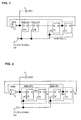
- Fig. 1 is a block diagram showing the circuit configuration of this first embodiment, which is a factor (2n + 1) frequency divider.
- MSD-FF1 and MSD-FF(n - 1) are respectively the first stage and final stage of a cascade-connected plurality of MSD-FFs.
- the circuit performs frequency division of a clock signal CK which is supplied from an external source to an input terminal 2, to obtain a final output signal OUT on an output terminal 1.
- Numeral 3 denotes a NOR gate.
- Fig. 2 shows the configuration of the first embodiment when implemented as a factor 3 frequency divider. This differs from the prior art factor 3 frequency divider of Fig. 8 in that a signal expressing the NOR function of the Q-terminal output signal from the master D-type latch of the second-stage MSD-FF2 and the Q-terminal output from the slave D-type latch of that MSD-FF2 is derived by the NOR gate 3, and in that the output signal from that NOR gate 3 constitutes the final output signal from the factor 3 frequency divider.
- Fig. 3 is a timing chart for describing the operation of this factor 3 frequency divider.
- the operation is as follows, with the signal designations M1, M2, S1 respectively having the same significances as for the prior art example of Fig. 8 described above, and S2 denoting the Q output signal from the slave D-type latch of MSD-FF2.
- the respective Q-terminal outputs in both of the MSD-FFs are initially all at the L level, then in that condition the output from the NOR gate 3, constituting the final output signal OUT, is at the H level.
- Signal M1 then goes to the H level at the first transition of the clock signal CK from the H to the L level, and signal 31 then goes to the H level at the succeeding transition of signal CK from the L to the H level.
- a signal is derived expressing the negated logic sum of the Q-terminal output signal from the master D-type latch of the final-stage MSD-FF and the Q-terminal output signal from the slave D-type latch of that final-stage MSD-FF, and that derived signal is applied to the D input terminal of the first-stage MSD-FF.
- that derived signal constitutes the final output signal from the frequency divider.
- the output signal from the odd number factor frequency divider is applied as a clock signal to a 90° phase splitter circuit which is implemented as a single MSD-FF, with the inverted Q output from the slave D-type latch applied to the D input terminal of the master D-type latch, as described above referring to Fig. 10A.
- the respective Q-terminal output signals from a master D-type latch and a slave D-type latch of that MSD-FF constitute the two final output signals from the phase splitter circuit.
- Fig. 4 shows the configuration of the second embodiment, which is assumed for simplicity of description to use a factor 3 frequency divider in accordance with the first embodiment of the invention. It is assumed that the circuit is for use in a radio apparatus such as a mobile radio apparatus, and that the clock signal which is supplied to the factor 3 frequency divider is a local oscillator signal, i.e., a signal whose frequency is three times that which is required for each of two quadrature modulation/demodulation signals which differ in phase by 90°.
- the clock signal which is supplied to the factor 3 frequency divider is a local oscillator signal, i.e., a signal whose frequency is three times that which is required for each of two quadrature modulation/demodulation signals which differ in phase by 90°.
- the resultant output signal from the factor 3 frequency divider is supplied to a phase splitter circuit that is constituted by a MSD-FF 6 formed of a master D-type latch 8 and slave D-type latch 7, with the inverted (/Q) output from the slave D-type latch 7 being supplied to the D input terminal of the master D-type latch 8, and with the output signals MQ, SQ from the Q terminals of the master D-type latch 8 and slave D-type latch 7 being respectively supplied to output terminals 4, 5 as the required pair of signals which differ in phase by 90°.
- a phase splitter circuit that is constituted by a MSD-FF 6 formed of a master D-type latch 8 and slave D-type latch 7, with the inverted (/Q) output from the slave D-type latch 7 being supplied to the D input terminal of the master D-type latch 8, and with the output signals MQ, SQ from the Q terminals of the master D-type latch 8 and slave D-type latch 7 being respectively supplied to output terminals 4, 5 as the required pair of signals which differ in phase by
- Fig. 5 is a timing chart of the operation of the circuit of Fig. 4. It can be understood from Fig. 5 that, since the duty ratio of the clock signal (i.e., output signal from NOR gate 3) that is supplied to the 90° phase splitter circuit is 1/2, the two output signals from the 90° phase splitter circuit correctly differ in phase from one another by 90°. Hence it is not necessary to use additional circuit components to correct the duty ratio of the clock signal supplied to the phase splitter circuit, or to apply phase correction to the output signals from the phase splitter circuit. The circuit scale can therefore be small, and the current consumption can be low. Hence, a mobile radio apparatus which utilizes such a circuit to derive quadrature modulation and demodulation signals can have an extended duration of use before battery replacement becomes necessary.
- the duty ratio of the clock signal i.e., output signal from NOR gate 3
Landscapes
- Manipulation Of Pulses (AREA)
- Stabilization Of Oscillater, Synchronisation, Frequency Synthesizers (AREA)
- Pulse Circuits (AREA)
Abstract
Description
Claims (4)
- An odd number factor frequency divider comprisinga plurality of master-slave D-type flip-flops connected in cascade and operating from the same clock signal, each master-slave D-type flip-flop formed of a master D-type latch and a slave D-type latch connected in cascade, with the master D-type latch synchronized with the clock signal and the slave D-type latch synchronized with the inverse of the clock signal,a NOR gate for producing an output signal expressing the negated logic sum of a Q-terminal output from a master D-type latch of a final stage of said cascade-connected plurality of master-slave D-type flip-flops and a Q-terminal output from a slave D-type latch of said final stage,means for applying said NOR gate output signal to a D input terminal of a master D-type latch of a master-slave D-type flip-flop of an initial stage of said cascade-connected plurality of master-slave D-type flip-flops, andmeans for outputting said NOR gate output signal as a final output signal of said frequency divider.
- A 90° phase splitter circuit comprisinga master-slave D-type flip-flop which operates from a clock signal constituted by a final output signal produced by an odd number factor frequency divider as claimed in claim 1,means for connecting an inverting Q-terminal output from a slave D-type latch of said master-slave D-type flip-flop to a D input terminal of a master D-type latch thereof, andmeans for outputting respective Q-terminal output signals from said master D-type latch and slave D-type latch, as final output signals of said 90° phase splitter circuit.
- A frequency divider method comprising:performing frequency division operation by supplying an externally derived signal, as a clock signal, to a circuit formed of a plurality of master-slave D-type flip-flops connected in cascade and each synchronized with the clock signal, each master-slave D-type flip-flop being formed of a master D-type latch and a slave D-type latch connected in cascade, with the master D-type latch synchronized with the clock signal and the slave D-type latch synchronized with the inverse of the clock signal,deriving a negated logic sum signal by inputting to a NOR gate a Q-terminal output from a master D-type latch of a final stage of said cascade-connected plurality of master-slave D-type flip-flops and a Q-terminal output from a slave D-type latch of said final stage, andapplying said negated logic sum signal to a D input terminal of a master D-type latch of a master-slave D-type flip-flop of an initial stage of said cascade-connected plurality of master-slave D-type flip-flops, while outputting said negated logic sum signal as a final output signal.
- A mobile radio apparatus incorporating a 90° phase splitter as claimed in claim 2.
Applications Claiming Priority (2)
| Application Number | Priority Date | Filing Date | Title |
|---|---|---|---|
| JP2001149584A JP2002344308A (en) | 2001-05-18 | 2001-05-18 | Odd number divider and 90 degree phase shifter using it |
| JP2001149584 | 2001-05-18 |
Publications (2)
| Publication Number | Publication Date |
|---|---|
| EP1267493A2 true EP1267493A2 (en) | 2002-12-18 |
| EP1267493A3 EP1267493A3 (en) | 2003-11-26 |
Family
ID=18994730
Family Applications (1)
| Application Number | Title | Priority Date | Filing Date |
|---|---|---|---|
| EP02006111A Withdrawn EP1267493A3 (en) | 2001-05-18 | 2002-03-18 | Odd-number factor frequency divider and 90 degrees phase splitter which operates from output signal of the frequency divider |
Country Status (4)
| Country | Link |
|---|---|
| US (1) | US20020171458A1 (en) |
| EP (1) | EP1267493A3 (en) |
| JP (1) | JP2002344308A (en) |
| CN (1) | CN1387322A (en) |
Families Citing this family (19)
| Publication number | Priority date | Publication date | Assignee | Title |
|---|---|---|---|---|
| JP2005064764A (en) * | 2003-08-08 | 2005-03-10 | Alps Electric Co Ltd | Direct conversion tuner |
| CN1320763C (en) * | 2003-10-20 | 2007-06-06 | 扬智科技股份有限公司 | Frequency division method with non-integer frequency division multiplier and related signal circuit |
| US7379723B2 (en) * | 2004-07-29 | 2008-05-27 | Silicon Laboratories Inc. | Local oscillator and mixer for transceiver |
| EP1776764B1 (en) * | 2004-08-06 | 2015-04-15 | Nxp B.V. | Frequency divider |
| US20060045202A1 (en) * | 2004-08-31 | 2006-03-02 | Aslam Rafi | Matching I and Q portions of a device |
| DE102005028119A1 (en) * | 2005-06-10 | 2006-12-14 | Atmel Germany Gmbh | Frequency divider circuit with a feedback shift register |
| CN101378258B (en) * | 2007-08-29 | 2010-09-29 | 中国科学院电子学研究所 | A modular frequency division unit and frequency divider |
| JP5654196B2 (en) * | 2008-05-22 | 2015-01-14 | ピーエスフォー ルクスコ エスエイアールエルPS4 Luxco S.a.r.l. | DLL circuit unit and semiconductor memory |
| TWI456493B (en) * | 2010-12-29 | 2014-10-11 | Silicon Motion Inc | Dividing method and dividing apparatus |
| CN102427363B (en) * | 2011-12-23 | 2015-02-04 | 上海贝岭股份有限公司 | Multiphase multimode frequency-dividing circuit with small frequency coefficient |
| CN103684425A (en) * | 2012-09-12 | 2014-03-26 | 比亚迪股份有限公司 | Dual-mode frequency divider circuit |
| TW201415805A (en) * | 2012-10-15 | 2014-04-16 | Keystone Semiconductor Corp | Frequency divider and frequency synthesizer circuit with the same |
| TW201415799A (en) * | 2012-10-15 | 2014-04-16 | Keystone Semiconductor Corp | Multi modulus frequency divider |
| JP2014135550A (en) * | 2013-01-08 | 2014-07-24 | New Japan Radio Co Ltd | Clock generation circuit |
| US20160079985A1 (en) * | 2014-09-16 | 2016-03-17 | Qualcomm Incorporated | Quadrature local oscillator phase synthesis and architecture for divide-by-odd-number frequency dividers |
| JP2018164151A (en) | 2017-03-24 | 2018-10-18 | 東芝メモリ株式会社 | Frequency divider circuit |
| CN113364449B (en) * | 2020-03-04 | 2024-10-01 | 川土微电子(深圳)有限公司 | Self-calibration frequency divider |
| CN117176140B (en) * | 2023-08-18 | 2024-03-19 | 上海奎芯集成电路设计有限公司 | Synchronous seven-frequency dividing circuit and seven-frequency dividing signal generation method |
| CN118157659B (en) * | 2024-05-09 | 2024-07-30 | 成都旋极星源信息技术有限公司 | Odd-number frequency dividing circuit |
Family Cites Families (2)
| Publication number | Priority date | Publication date | Assignee | Title |
|---|---|---|---|---|
| US5375258A (en) * | 1992-12-07 | 1994-12-20 | Motorola, Inc. | Circuit for generating signals in phase quadrature and associated method therefor |
| DE4340966C1 (en) * | 1993-12-01 | 1995-01-19 | Siemens Ag | Circuit arrangement for generating even duty ratios |
-
2001
- 2001-05-18 JP JP2001149584A patent/JP2002344308A/en active Pending
-
2002
- 2002-03-18 EP EP02006111A patent/EP1267493A3/en not_active Withdrawn
- 2002-03-25 US US10/103,868 patent/US20020171458A1/en not_active Abandoned
- 2002-05-17 CN CN02120000.9A patent/CN1387322A/en active Pending
Also Published As
| Publication number | Publication date |
|---|---|
| EP1267493A3 (en) | 2003-11-26 |
| CN1387322A (en) | 2002-12-25 |
| US20020171458A1 (en) | 2002-11-21 |
| JP2002344308A (en) | 2002-11-29 |
Similar Documents
| Publication | Publication Date | Title |
|---|---|---|
| EP1267493A2 (en) | Odd-number factor frequency divider and 90 degrees phase splitter which operates from output signal of the frequency divider | |
| TWI429188B (en) | Dual-modulus prescaler circuit operating at a very high frequency | |
| JP4044819B2 (en) | Phase switched dual-modulus prescaler circuit with means for reducing power consumption | |
| US20040075479A1 (en) | Reducing power and area consumption of gated clock enabled flip flops | |
| KR970072709A (en) | Frequency multiplication circuit | |
| JP2004516768A (en) | Frequency divider with reduced power consumption, device based on the divider, and method for power efficient frequency divider | |
| US7680238B2 (en) | Frequency divider circuit | |
| CN116566383B (en) | Synchronous five-frequency dividing circuit and five-frequency dividing signal generation method | |
| US20060109035A1 (en) | Clock frequency divider circuit | |
| US7535277B2 (en) | Frequency dividing phase shift circuit | |
| US6067339A (en) | Frequency divider with lower power consumption | |
| EP2474094B1 (en) | Driving a mixer with a differential lo signal having at least three signal levels | |
| US4639554A (en) | Dual-tone multiple-frequency-signal generating apparatus | |
| TW200428794A (en) | Frequency divider for RF transceiver | |
| US9774333B2 (en) | Counter circuit | |
| US5969548A (en) | Frequency divider with low power consumption | |
| JP2008005446A (en) | Frequency divider and control method thereof | |
| KR100671749B1 (en) | Clock divider | |
| KR100336756B1 (en) | Clock dividing circuit | |
| JPH09261019A (en) | Synchronization circuit | |
| EP4418536A1 (en) | A circuitry and a method for generating a set of output clock signals | |
| KR100336753B1 (en) | State clock generator | |
| US10027280B1 (en) | Inductor-less local oscillator generation apparatus | |
| JP3178459B2 (en) | Operation clock frequency switching circuit | |
| JPH08328687A (en) | Clock switching circuit |
Legal Events
| Date | Code | Title | Description |
|---|---|---|---|
| PUAI | Public reference made under article 153(3) epc to a published international application that has entered the european phase |
Free format text: ORIGINAL CODE: 0009012 |
|
| AK | Designated contracting states |
Kind code of ref document: A2 Designated state(s): AT BE CH CY DE DK ES FI FR GB GR IE IT LI LU MC NL PT SE TR |
|
| AX | Request for extension of the european patent |
Free format text: AL;LT;LV;MK;RO;SI |
|
| PUAL | Search report despatched |
Free format text: ORIGINAL CODE: 0009013 |
|
| AK | Designated contracting states |
Kind code of ref document: A3 Designated state(s): AT BE CH CY DE DK ES FI FR GB GR IE IT LI LU MC NL PT SE TR |
|
| AX | Request for extension of the european patent |
Extension state: AL LT LV MK RO SI |
|
| RIC1 | Information provided on ipc code assigned before grant |
Ipc: 7H 03K 19/096 B Ipc: 7H 03K 19/00 A |
|
| AKX | Designation fees paid | ||
| REG | Reference to a national code |
Ref country code: DE Ref legal event code: 8566 |
|
| STAA | Information on the status of an ep patent application or granted ep patent |
Free format text: STATUS: THE APPLICATION IS DEEMED TO BE WITHDRAWN |
|
| 18D | Application deemed to be withdrawn |
Effective date: 20040527 |