EP1267423A2 - Light-emitting device sealing - Google Patents
Light-emitting device sealing Download PDFInfo
- Publication number
- EP1267423A2 EP1267423A2 EP02013470A EP02013470A EP1267423A2 EP 1267423 A2 EP1267423 A2 EP 1267423A2 EP 02013470 A EP02013470 A EP 02013470A EP 02013470 A EP02013470 A EP 02013470A EP 1267423 A2 EP1267423 A2 EP 1267423A2
- Authority
- EP
- European Patent Office
- Prior art keywords
- light
- emitting element
- base member
- sealing member
- emitting device
- Prior art date
- Legal status (The legal status is an assumption and is not a legal conclusion. Google has not performed a legal analysis and makes no representation as to the accuracy of the status listed.)
- Granted
Links
- 0 CC(C)N*c1ccc(*C(C)(C)C)cc1 Chemical compound CC(C)N*c1ccc(*C(C)(C)C)cc1 0.000 description 1
Images


Classifications
-
- H—ELECTRICITY
- H10—SEMICONDUCTOR DEVICES; ELECTRIC SOLID-STATE DEVICES NOT OTHERWISE PROVIDED FOR
- H10H—INORGANIC LIGHT-EMITTING SEMICONDUCTOR DEVICES HAVING POTENTIAL BARRIERS
- H10H20/00—Individual inorganic light-emitting semiconductor devices having potential barriers, e.g. light-emitting diodes [LED]
- H10H20/80—Constructional details
- H10H20/85—Packages
- H10H20/8506—Containers
-
- H—ELECTRICITY
- H10—SEMICONDUCTOR DEVICES; ELECTRIC SOLID-STATE DEVICES NOT OTHERWISE PROVIDED FOR
- H10H—INORGANIC LIGHT-EMITTING SEMICONDUCTOR DEVICES HAVING POTENTIAL BARRIERS
- H10H20/00—Individual inorganic light-emitting semiconductor devices having potential barriers, e.g. light-emitting diodes [LED]
- H10H20/80—Constructional details
- H10H20/85—Packages
- H10H20/852—Encapsulations
- H10H20/854—Encapsulations characterised by their material, e.g. epoxy or silicone resins
-
- H—ELECTRICITY
- H10—SEMICONDUCTOR DEVICES; ELECTRIC SOLID-STATE DEVICES NOT OTHERWISE PROVIDED FOR
- H10H—INORGANIC LIGHT-EMITTING SEMICONDUCTOR DEVICES HAVING POTENTIAL BARRIERS
- H10H20/00—Individual inorganic light-emitting semiconductor devices having potential barriers, e.g. light-emitting diodes [LED]
- H10H20/80—Constructional details
- H10H20/882—Scattering means
-
- H—ELECTRICITY
- H10—SEMICONDUCTOR DEVICES; ELECTRIC SOLID-STATE DEVICES NOT OTHERWISE PROVIDED FOR
- H10W—GENERIC PACKAGES, INTERCONNECTIONS, CONNECTORS OR OTHER CONSTRUCTIONAL DETAILS OF DEVICES COVERED BY CLASS H10
- H10W72/00—Interconnections or connectors in packages
- H10W72/071—Connecting or disconnecting
- H10W72/075—Connecting or disconnecting of bond wires
- H10W72/07551—Connecting or disconnecting of bond wires characterised by changes in properties of the bond wires during the connecting
- H10W72/07554—Connecting or disconnecting of bond wires characterised by changes in properties of the bond wires during the connecting changes in dispositions
-
- H—ELECTRICITY
- H10—SEMICONDUCTOR DEVICES; ELECTRIC SOLID-STATE DEVICES NOT OTHERWISE PROVIDED FOR
- H10W—GENERIC PACKAGES, INTERCONNECTIONS, CONNECTORS OR OTHER CONSTRUCTIONAL DETAILS OF DEVICES COVERED BY CLASS H10
- H10W72/00—Interconnections or connectors in packages
- H10W72/50—Bond wires
- H10W72/541—Dispositions of bond wires
- H10W72/547—Dispositions of multiple bond wires
-
- H—ELECTRICITY
- H10—SEMICONDUCTOR DEVICES; ELECTRIC SOLID-STATE DEVICES NOT OTHERWISE PROVIDED FOR
- H10W—GENERIC PACKAGES, INTERCONNECTIONS, CONNECTORS OR OTHER CONSTRUCTIONAL DETAILS OF DEVICES COVERED BY CLASS H10
- H10W90/00—Package configurations
- H10W90/701—Package configurations characterised by the relative positions of pads or connectors relative to package parts
- H10W90/751—Package configurations characterised by the relative positions of pads or connectors relative to package parts of bond wires
- H10W90/754—Package configurations characterised by the relative positions of pads or connectors relative to package parts of bond wires between a chip and a stacked insulating package substrate, interposer or RDL
Definitions
- the present invention relates to a light-emitting device and particularly to a device using a light-emitting element which emits light in a relatively short wavelength range.
- the light-emitting device according to the invention can be used as a light source for illumination or as a light source for various kinds of display devices.
- a device configured as shown in Fig. 5 is known as a light-emitting device using a light-emitting element.
- Fig. 5 typically shows an SMD (Surface Mounted Device) type LED 100.
- the LED 100 is produced as follows.
- a light-emitting element 110 is disposed into a cup-like portion 150 formed by a combination of a substrate 120 and a reflector (casing) 130.
- the cup-like portion 150 is filled with a sealing member 140 (light-transmissive resin).
- the reflector 130 is made of a polymer resin containing a white filler such as titanium oxide.
- the sealing member 140 is generally made of an epoxy resin.
- the light-emitting element used in the SMD type LED exhibits an emission peak wavelength in a relatively long wavelength range such as a red region.
- the epoxy resin used as the sealing member is relatively durable against light emitted from the light-emitting element. Accordingly, the color in the epoxy resin may be more or less changed in long-term use but the degree of the change of the color is small.
- the sealing member in order to secure the stability and reliability of the light-emitting device, it is necessary to form the sealing member in a state in which no gap is generated between the sealing member and a base member (including a reflector) on which the light-emitting element is mounted. That is, sufficient adhesion (close contact) is required between the sealing member and the base member.
- the inventors have examined the material of the sealing member and the base member in consideration of the problem. As a result, it has been found that silicone as the material of the sealing member exhibits very high durability against light in a short wavelength region. From the point of view of adhesion between the sealing member and the base member, the inventors also have made examination. According to the examination result, it has been found that good adhesion is obtained between the sealing member and the base member when a polyamide-based resin is used as the base member in the case where silicone is used as the sealing member.
- the invention is based on the findings and is configured as follows.
- a light-emitting device including a semiconductor light-emitting element, a base member provided so that the semiconductor light-emitting element is mounted on the base member, and a sealing member provided so that the semiconductor light-emitting element is coated with the sealing member, wherein:
- a semiconductor light-emitting element exhibiting an emission peak wavelength in a wavelength range of not longer than 500 nm is preferably used as the semiconductor light-emitting element. More preferably, a semiconductor light-emitting element exhibiting an emission peak wavelength in a wavelength range of not longer than 400 nm may be used as the semiconductor light-emitting element. Further preferably, a semiconductor light-emitting element exhibiting an emission peak wavelength in a wavelength range of from 370 to 390 nm may be used as the semiconductor light-emitting element.
- a semiconductor light-emitting element having a plurality of emission peaks may be used as well as a semiconductor light-emitting element having a single emission peak.
- the semiconductor light-emitting element may exhibit one emission peak or two or more emission peaks in a wavelength region longer than 500 nm.
- the configuration of the semiconductor light-emitting element is not particularly limited.
- a semiconductor light-emitting element having a light-emitting layer made of a Group III nitride compound semiconductor can be used.
- Group III nitride compound semiconductors are generally expressed as quarternary compounds represented by the general formula Al X Ga Y In 1-X-Y N (0 ⁇ X ⁇ 1, 0 ⁇ Y ⁇ 1, 0 ⁇ X+Y ⁇ 1), which includes so-called binary compounds such as AlN, GaN and InN, and so-called ternary compounds such as Al x Ga 1-x N, Al x In 1-x N and Ga x In 1-x N (0 ⁇ x ⁇ 1).
- the group III elements may be partially replaced by boron (B), thallium (Tl), etc.
- the nitrogen (N) may be partially replaced by phosphorus (P), arsenic (As), antimony (Sb), bismuth (Bi), etc.
- the light-emitting layer may contain any optional dopant.
- the base member is a member on which the semiconductor light-emitting element is mounted. At least one portion of the base member is made of a polyamide-based resin.
- base member in this specification includes a base member as a single member, and a base member as a combination of a plurality of members.
- An example of the former base member as a single member may be a member molded out of a specific material so that a cavity portion (cup-like portion) is formed on one surface side. In this case, a frame may be inserted in the base member.
- an example of the later base member as a combination of a plurality of members may be a combination of a casing and a substrate.
- the base member can be formed so that a casing having a desired shape is bonded onto a substrate in order to form a cavity portion (cup-like portion) .
- a base member made of only a substantially flat substrate may be used as the base member.
- the "cavity portion (cup-like portion)" formed in the base member means a portion which has a bottom portion and a side portion and is constituted by a space shaped like a form in which the area of a section in a direction perpendicular to the optical axis increases continuously or stepwise from the bottom portion to the light-extracting direction of the light-emitting device.
- the shapes of the bottom portion and the side portion are not particularly limited if this condition is satisfied.
- At least one portion of the base member is made of a polyamide-based resin.
- adhesion between a sealing member (which will be described later) and the surface of the base member is made so high that both stability and reliability of the light-emitting device are improved.
- the whole surface of the base member touching the sealing member is made of this material.
- the whole surface of the base member constituting the cup-like portion is made of this material, in consideration of facilitation of producing the base member and facilitation of setting the condition for forming the sealing member.
- the base member as a whole may be made of this material. Such a base member can be produced by molding using this material.
- the base member as a whole can be made of a polyamide-based resin.
- both the substrate and the casing may be made of a polyamide-based resin.
- the base member may be formed by use of a plurality of polyamide-based resins different in composition.
- the base member may contain a light-reflective filler. In this manner, light emitted from the light-emitting element can be reflected with high efficiency by the surface of the base member, so that luminance of light emitted from the light-emitting device is improved.
- an aromatic polyamide-based resin selected from the polyamide-based resins is used.
- the "aromatic polyamide-based resin” means a resin of polyamide having an aromatic ring as a main chain.
- the aromatic polyamide-based resin is not particularly limited in kind.
- an aromatic Nylon resin represented by the following general formula:
- the light-reflective filler is not particularly limited in kind.
- a material high in light reflectance is preferably selected in order to enhance reflectance of the light by the surface of the base member to thereby improve luminance of light emitted from the light-emitting device.
- titanium oxide, or potassium titanate can be used.
- the surface of the base member irradiated with light from the light-emitting element is preferably made as smooth as possible. This is because specular reflection occurs more easily as the surface becomes smoother, that is, because the quantity of light reflected by the surface of the base member and radiated out can be increased.
- the angle of the base member surface forming the cup-like portion can be designed in consideration of light reflecting efficiency in the direction of the optical axis. The angle is preferably selected to be in a range of from 20° to 60°, more preferably in a range of from 20° to 50°, with respect to the optical axis of the light-emitting element.
- the sealing member is a member which is formed so that the light-emitting element is covered with the member.
- the sealing member is mainly provided for protecting the light-emitting element from external environment.
- At least one portion of the sealing member is made of silicone. That is, the sealing member is constituted by a material at least containing silicone resin, silicone rubber, and/or silicone elastomer.
- silicone rubber is used as one material of the sealingmember.
- a sealing member made of silicone rubber is used. In this case, it is preferable that silicone rubber exhibiting high transmittance to light emitted from the light-emitting element is used. When such a material is used, light emitted from the light-emitting element can be radiated out efficiently.
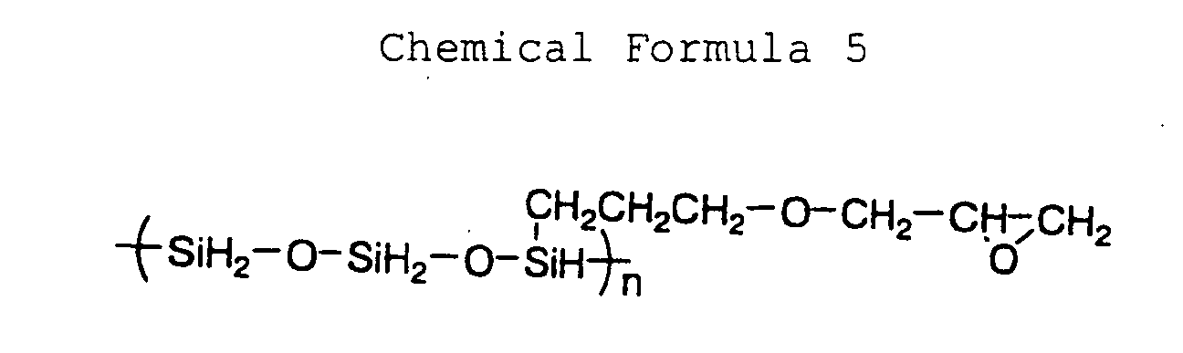
- the sealing member may contain an epoxy group. That is, as a preferred mode, the sealing member is made of silicone rubber containing an epoxy group. In this manner, sufficient adhesion between the sealing member and the base member is obtained, so that both stability and reliability of the light-emitting device are improved. This effect is guessed to be for the following reason. That is, because the polyamide-based resin used as the material of the base member surface contains an amide group in its molecule, a hydrogen atom in the amide group in the base member surface and an oxygen atom in the epoxy group in the sealing member can form a hydrogen bond. In addition, terminal amine in the polyamide-based resin and the epoxy group in the sealing member can form a covalent bond. The epoxy group also plays as a role of a curing agent for the sealing member.
- the epoxy group may exist independent of the silicone molecule or may exist as a part of the side chain of the silicone molecule if the epoxy group may be contained in the sealing member.
- any suitable material in consideration of transmittance to light emitted from the light-emitting element, hardness in a cured state, handling property, etc. can be used as the material of the sealing member.
- silicone rubber obtained by crosslinkage of a mixture of a chief agent and a curing agent represented by the following general formulae can be used as the material of the sealing member.
- the sealing member may be provided so that a plurality of layers made of different materials respectively are formed by lamination on the light-emitting element.
- a layer made of a material durable against light emitted from the light-emitting element such as a layer of silicone rubber containing an epoxy group, is provided near the light-emitting element.
- the sealing member may contain a fluorescent substance.
- a fluorescent substance When the fluorescent substance is used, a part of light emitted from the light-emitting element can be converted into light at a different wavelength, that is, the color of light emitted from the light-emitting device can be changed or corrected.
- An arbitrary fluorescent substance may be used if it can be excited by light emitted from the light-emitting element.
- the fluorescent substance is selected in consideration of the color of light emitted from the light-emitting device, the durability of the light-emitting device, etc.
- the fluorescent substance may be dispersed uniformly in the sealing member or may be localized in a partial region. When, for example, the fluorescent substance is localized in the vicinity of the light-emitting element, the fluorescent substance can be efficiently irradiated with light emitted from the light-emitting element.
- a combination of a plurality of kinds of fluorescent substances may be contained in the sealing member.
- a fluorescent substance which emits light when excited by light from the light-emitting element and a fluorescent substance which emits light when excited by light from the fluorescent substance can be used in combination.
- the sealing member contains a light-diffusing material
- light diffusion in the sealing member can be promoted so that emission unevenness can be reduced.
- the light-diffusing material is used to promote color mixing of light from the light-emitting element and light from the fluorescent substance to thereby reduce emission color unevenness.
- Fig. 1 is a view typically showing a section of a light-emitting diode 1.
- the light-emitting diode 1 typically includes a light-emitting element 10, a substrate 20, a reflector 30, and a sealing member 40.
- the combination of the substrate 20 and the reflector 30 is equivalent to the casing described above.
- the light-emitting diode 1 further includes a Zener diode not shown but provided for withstanding electrostatic voltage.
- the light-emitting element 10 is a Group III nitride compound semiconductor light-emitting element.
- Fig. 2 typically shows the configuration of the light-emitting element 10.
- the light-emitting element 10 includes a sapphire substrate, and a plurality of Group III nitride compound semiconductor layers laminated on the sapphire substrate.
- the light-emitting element 10 has an emission peak wavelength at about 380 nm. Specifications of respective layers in the light-emitting element 10 are as follows.
- Layer Composition p-type semiconductor layer 15 p-GaN Mg
- n-type semiconductor layer 13 n-GaN Si Buffer layer 12 AlN Substrate 11 Sapphire
- n-type semiconductor layer 13 made of GaN doped with Si as n-type impurities is formed on the substrate 11 through the buffer layer 12.
- the material of the substrate 11 is not limited to sapphire.
- the material of the substrate 11 which can be used include sapphire, spinel, silicon, silicon carbide, zinc oxide, gallium phosphate, gallium arsenide, magnesium oxide, manganese oxide, and Group III nitride compound semiconductor monocrystal.
- the buffer layer 12 is made of AlN by an MOCVD method, the material of the buffer layer 12 is not limited thereto.
- GaN, InN, AlGaN, InGaN, or AlInGaN may be used as the material of the buffer layer 12.
- Amolecular beam epitaxy method (MBE method) a halide vapor phase epitaxy method (HVPE method), a sputtering method, an ion-plating method, an electron shower method, etc. may be used as the method for producing. the buffer layer 12.
- HVPE method halide vapor phase epitaxy method
- a sputtering method an ion-plating method
- an electron shower method etc.
- the substrate and the buffer layer may be removed in accordance with necessity after the formation of the semiconductor element.
- the invention may be applied also to the case where AlGaN, InGaN or AlInGaN is used as the material of the n-type semiconductor layer 13.
- this embodiment shows the case where the n-type semiconductor layer 13 is doped with Si as n-type impurities, the invention may be applied also to the case where Ge, Se, Te, or C is used as n-type impurities.
- the n-type semiconductor layer 13 may be of a double-layer structure with an n - layer of low electron density on the light-emitting layer-containing layer 14 side and an n + layer of high electron density on the buffer layer 12 side.
- the layer 14 containing a light-emitting layer may contain a quantum well structure (multiple quantum well structure or single quantum well structure).
- the structure of the light-emitting element may be of a single hetero type, a double hetero type or a homo-junction type.
- the layer 14 may contain a Group III nitride compound semiconductor layer provided on the p-type semiconductor layer 15 side, doped with an acceptor such as magnesium and having a wide band gap. This arrangement is made for effectively preventing electrons injected into the light-emitting layer-containing layer 14 from diffusing into the p-type layer 15.
- the p-type semiconductor layer 15 made of GaN doped with Mg as p-type impurities is formed on the light-emitting layer-containing layer 14.
- the p-type semiconductor layer 15 may be made of AlGaN, InGaN or InAlGaN. Zn, Be, Ca, Sr or Ba may be used as p-type impurities instead.
- the p-type semiconductor layer 15 may be of a double-layer structure with a p - layer of low hole density on the light-emitting layer-containing layer 14 side and a p + layer of high hole density on the electrode side.
- each of the Group III nitride compound semiconductor layers may be formed by an MOCVD method in a general condition or may be formed by a method such as a molecular beam epitaxy method (MBE method) , a halide vapor phase epitaxy method (HVPE method) , a sputtering method, an ion-plating method, or an electron shower method.
- MBE method molecular beam epitaxy method
- HVPE method halide vapor phase epitaxy method
- sputtering method an ion-plating method
- an electron shower method an electron shower method
- the n-electrode 18 is composed of two layers of Al and V. After the p-type semiconductor layer 15 is formed, the p-type semiconductor layer 15, the layer 14 and the n-type semiconductor layer 13 are partially removed by etching. In this condition, the n-electrode 18 is formed on the n-type semiconductor layer 13 by vapor deposition.
- the light-transmissive electrode 16 is a thin film containing gold and is laminated on the p-type semiconductor layer 15.
- the p-electrode 17 is also made of a material containing gold and is formed on the light-transmissive electrode 16 by vapor deposition.
- a step of separating the substrate into chips is carried out.
- the substrate 20 is an electrically insulating substrate having a surface on which a desired wiring pattern is printed.
- the light-emitting element 10 is mounted in a desired position of the substrate 20.
- the reflector 30 is disposed on the substrate 20 so that a cup-like portion 50 is formed by a combination of the reflector 30 and a part of the surface of the substrate 20.
- the reflector 30 is made of an aromatic Nylon resin containing potassium titanate dispersed therein uniformly and is molded so that a surface forming the cup-like portion 50 is inclined at a desired angle to the optical axis .
- the inclination angle of the surface is selected to be about 30° to the optical axis of the light-emitting element 10.
- the sealing member 40 is made of silicone rubber containing an epoxy group as a side chain.
- the LED 1 configured as described above is produced as follows.
- the reflector 30 is disposed on the substrate 20. Then, the light-emitting element 10 is mounted, and the electrodes of the light-emitting element 10 are connected to the wiring pattern on the substrate 20 by leads. Then, the surface of the light-emitting element 10 is coated with ceramics not shown. Then, the following chief agent and curing agent are mixed with each other to prepare liquid silicone rubber. The liquid silicone rubber is potted in the cup-like portion 50.
- the silicone rubber is heated to about 150°C to be thermally cured.
- the silicone rubber is cured in a state in which the silicone rubber is fitted and bonded to the surface of the reflector 30. Then, heat radiation is performed in air.
- Fig. 3 is a view typically showing the configuration of a light-emitting diode 2 as another embodiment of the invention.
- members the same as those of the light-emitting diode 1 are referenced correspondingly.
- a lead frame 80 is used instead of the substrate.
- the light-emitting element 10 is mounted on the lead frame 80.
- the configuration except this point is the same as that of the light-emitting diode 1.
- Fig. 4 is a view typically showing the configuration of a light-emitting diode 3 as a further embodiment of the invention.
- members the same as those of the light-emitting diode 1 are referenced correspondingly.
- a substrate 70 made of a polyamide-based resin is used in the light-emitting diode 3.
- Desired wiring 71 is applied on the substrate 70.
- the light-emitting diode 3 does not use any casing (reflector) .
- a sealing member 60 substantially shaped like a rectangle in section is formed so that the light-emitting element 10 is covered with the sealing member 60.
- the sealing member 60 can be formed by a method including the steps of: mounting the light-emitting element 10 on the substrate 70; and performing molding by using a desired mold.
- a sealing member 60 molded into a desired shape in advance may be prepared so that the sealing member 60 is bonded to the substrate 70 so that the light-emitting element 10 is covered with the sealing member 60.
- SMD type light-emitting diodes have been described as embodiments of the invention, the invention may be applied also to so-called round type light-emitting diodes in each of which a light-emitting element is mounted on a lead frame having a cup-like portion and in which the light-emitting element and the lead frame are partially covered with a sealing member.
- the invention may be applied to flip chip type light-emitting diodes in each of which a light-emitting element is mounted on a substrate or a lead frame in the form of a so-called flip chip.
Landscapes
- Led Device Packages (AREA)
- Compositions Of Macromolecular Compounds (AREA)
- Led Devices (AREA)
Abstract
Description


| Layer | Composition |
| p-type semiconductor layer 15 | p-GaN : |
| Layer | |
| 14 containing a light-emitting layer4 | Inclusive of InGaN layer |
| n-type semiconductor layer 13 | n-GaN : |
| Buffer layer | |
| 12 | |
| Substrate | |
| 11 | Sapphire |

Claims (10)
- A light-emitting device comprising:wherein at least one portion of said base member is made of a polyamide-based resin, and at least one portion of said sealing member is made of silicone.a semiconductor light-emitting element (10);a base member (20, 30; 30, 80; 70, 71) provided so that said semiconductor light-emitting element is mounted on said base member; anda sealing member (40; 60) provided so that said semiconductor light-emitting element is coated with said sealing member;
- A light-emitting device according to claim 1, wherein said base member includes a casing (30) made of a polyamide-based resin, and a substrate (20) made of another material and bonded to said casing so that a cavity portion (50) is formed.
- A light-emitting device according to claim 1, wherein said base member (30, 80) is made of a polyamide-based resin containing a lead frame (80) as an insert.
- A light-emitting device according to claim 1, wherein said base member includes a substrate (70) made of a polyamide-based resin.
- A light-emitting device according to one of claims 1 to 4, wherein said semiconductor light-emitting element (10) exhibits an emission peak in a wavelength range of not longer than 500 nm.
- A light-emitting device according to one of claims 1 to 5, wherein said polyamide-based resin is an aromatic Nylon resin.
- A light-emitting device according to one of claims 1 to 6, wherein said silicone contains an epoxy group.
- A light-emitting device according to one of the claims 1 to 7, wherein said silicone contains an epoxy group as a side chain.
- A light-emitting device according to one of claims 1 to 8, wherein said semiconductor light-emitting element exhibits an emission peak in a wavelength range of not longer than 400 nm.
- A light-emitting device according to one of claims 1 to 9, wherein said polyamide-based resin contains a light-reflective filler.
Applications Claiming Priority (2)
| Application Number | Priority Date | Filing Date | Title |
|---|---|---|---|
| JP2001182544A JP2002374007A (en) | 2001-06-15 | 2001-06-15 | Light emitting device |
| JP2001182544 | 2001-06-15 |
Publications (3)
| Publication Number | Publication Date |
|---|---|
| EP1267423A2 true EP1267423A2 (en) | 2002-12-18 |
| EP1267423A3 EP1267423A3 (en) | 2004-06-23 |
| EP1267423B1 EP1267423B1 (en) | 2006-03-22 |
Family
ID=19022633
Family Applications (1)
| Application Number | Title | Priority Date | Filing Date |
|---|---|---|---|
| EP02013470A Expired - Lifetime EP1267423B1 (en) | 2001-06-15 | 2002-06-14 | Light-emitting diode sealing |
Country Status (5)
| Country | Link |
|---|---|
| US (1) | US6680490B2 (en) |
| EP (1) | EP1267423B1 (en) |
| JP (1) | JP2002374007A (en) |
| DE (1) | DE60209964T8 (en) |
| TW (1) | TW544957B (en) |
Cited By (5)
| Publication number | Priority date | Publication date | Assignee | Title |
|---|---|---|---|---|
| WO2005064696A1 (en) * | 2003-12-30 | 2005-07-14 | Osram Opto Semiconductors Gmbh | Radiation-emitting and/or radiation-receiving semiconductor component and method for the production thereof |
| WO2005093862A3 (en) * | 2004-03-26 | 2006-04-27 | Matsushita Electric Industrial Co Ltd | Led mounting module, led module, manufacturing method of led mounting module, and manufacturing method of led module |
| WO2007006378A1 (en) * | 2005-07-08 | 2007-01-18 | Tridonic Optoelectronics Gmbh | Optoelectronic components comprising adhesive |
| EP1684345B1 (en) * | 2005-01-21 | 2013-09-25 | Stanley Electric Co., Ltd. | Surface mount semiconductor device |
| EP1939949B1 (en) * | 2005-09-30 | 2017-10-25 | Nichia Corporation | Light emitting device and backlight unit using the same |
Families Citing this family (57)
| Publication number | Priority date | Publication date | Assignee | Title |
|---|---|---|---|---|
| JP2004056088A (en) * | 2002-05-31 | 2004-02-19 | Toyoda Gosei Co Ltd | Group III nitride compound semiconductor light emitting device |
| JP2004055855A (en) * | 2002-07-19 | 2004-02-19 | Toyoda Gosei Co Ltd | Communication device |
| US20040137656A1 (en) * | 2003-01-15 | 2004-07-15 | Gurbir Singh | Low thermal resistance light emitting diode package and a method of making the same |
| JP4721625B2 (en) * | 2003-01-29 | 2011-07-13 | 旭化成ケミカルズ株式会社 | Light emitting diode |
| DE10307800A1 (en) * | 2003-02-24 | 2004-09-02 | Vishay Semiconductor Gmbh | Semiconductor device |
| DE10361801A1 (en) * | 2003-12-30 | 2005-08-04 | Osram Opto Semiconductors Gmbh | Radiation emitting and/or radiation receiving semiconductor element with a semiconductor chip useful in LED technology, and in reaction-flow processes and surface mounting technology (SMT) |
| JP4516337B2 (en) * | 2004-03-25 | 2010-08-04 | シチズン電子株式会社 | Semiconductor light emitting device |
| US7355284B2 (en) * | 2004-03-29 | 2008-04-08 | Cree, Inc. | Semiconductor light emitting devices including flexible film having therein an optical element |
| US7201497B2 (en) * | 2004-07-15 | 2007-04-10 | Lumination, Llc | Led lighting system with reflective board |
| US20060131709A1 (en) * | 2004-12-21 | 2006-06-22 | Caron Michael R | Semiconductor die positioning system and a method of bonding a semiconductor die to a substrate |
| US9070850B2 (en) | 2007-10-31 | 2015-06-30 | Cree, Inc. | Light emitting diode package and method for fabricating same |
| US9793247B2 (en) * | 2005-01-10 | 2017-10-17 | Cree, Inc. | Solid state lighting component |
| US7821023B2 (en) | 2005-01-10 | 2010-10-26 | Cree, Inc. | Solid state lighting component |
| US8669572B2 (en) * | 2005-06-10 | 2014-03-11 | Cree, Inc. | Power lamp package |
| US7772604B2 (en) | 2006-01-05 | 2010-08-10 | Illumitex | Separate optical device for directing light from an LED |
| US8044412B2 (en) | 2006-01-20 | 2011-10-25 | Taiwan Semiconductor Manufacturing Company, Ltd | Package for a light emitting element |
| US7675145B2 (en) * | 2006-03-28 | 2010-03-09 | Cree Hong Kong Limited | Apparatus, system and method for use in mounting electronic elements |
| US8748915B2 (en) * | 2006-04-24 | 2014-06-10 | Cree Hong Kong Limited | Emitter package with angled or vertical LED |
| US7635915B2 (en) * | 2006-04-26 | 2009-12-22 | Cree Hong Kong Limited | Apparatus and method for use in mounting electronic elements |
| US8735920B2 (en) | 2006-07-31 | 2014-05-27 | Cree, Inc. | Light emitting diode package with optical element |
| US8367945B2 (en) * | 2006-08-16 | 2013-02-05 | Cree Huizhou Opto Limited | Apparatus, system and method for use in mounting electronic elements |
| US7763478B2 (en) * | 2006-08-21 | 2010-07-27 | Cree, Inc. | Methods of forming semiconductor light emitting device packages by liquid injection molding |
| US20090275266A1 (en) * | 2006-10-02 | 2009-11-05 | Illumitex, Inc. | Optical device polishing |
| WO2008042351A2 (en) | 2006-10-02 | 2008-04-10 | Illumitex, Inc. | Led system and method |
| JP5380774B2 (en) * | 2006-12-28 | 2014-01-08 | 日亜化学工業株式会社 | Surface mount type side surface light emitting device and manufacturing method thereof |
| US9711703B2 (en) * | 2007-02-12 | 2017-07-18 | Cree Huizhou Opto Limited | Apparatus, system and method for use in mounting electronic elements |
| CN101388161A (en) * | 2007-09-14 | 2009-03-18 | 科锐香港有限公司 | LED surface mounting device and LED display incorporating the same |
| US10256385B2 (en) | 2007-10-31 | 2019-04-09 | Cree, Inc. | Light emitting die (LED) packages and related methods |
| USD615504S1 (en) | 2007-10-31 | 2010-05-11 | Cree, Inc. | Emitter package |
| US8866169B2 (en) * | 2007-10-31 | 2014-10-21 | Cree, Inc. | LED package with increased feature sizes |
| USD633631S1 (en) | 2007-12-14 | 2011-03-01 | Cree Hong Kong Limited | Light source of light emitting diode |
| USD634863S1 (en) | 2008-01-10 | 2011-03-22 | Cree Hong Kong Limited | Light source of light emitting diode |
| JP2011512037A (en) * | 2008-02-08 | 2011-04-14 | イルミテックス, インコーポレイテッド | System and method for emitter layer shaping |
| US8049230B2 (en) * | 2008-05-16 | 2011-11-01 | Cree Huizhou Opto Limited | Apparatus and system for miniature surface mount devices |
| US9425172B2 (en) * | 2008-10-24 | 2016-08-23 | Cree, Inc. | Light emitter array |
| US8791471B2 (en) | 2008-11-07 | 2014-07-29 | Cree Hong Kong Limited | Multi-chip light emitting diode modules |
| TW201034256A (en) * | 2008-12-11 | 2010-09-16 | Illumitex Inc | Systems and methods for packaging light-emitting diode devices |
| JP2010171379A (en) * | 2008-12-25 | 2010-08-05 | Seiko Instruments Inc | Light-emitting device |
| KR20100080423A (en) * | 2008-12-30 | 2010-07-08 | 삼성엘이디 주식회사 | Light emitting device package and method of fabricating thereof |
| US8368112B2 (en) | 2009-01-14 | 2013-02-05 | Cree Huizhou Opto Limited | Aligned multiple emitter package |
| US8415692B2 (en) * | 2009-07-06 | 2013-04-09 | Cree, Inc. | LED packages with scattering particle regions |
| US8598809B2 (en) * | 2009-08-19 | 2013-12-03 | Cree, Inc. | White light color changing solid state lighting and methods |
| US8449128B2 (en) * | 2009-08-20 | 2013-05-28 | Illumitex, Inc. | System and method for a lens and phosphor layer |
| US8585253B2 (en) | 2009-08-20 | 2013-11-19 | Illumitex, Inc. | System and method for color mixing lens array |
| DE102009055786A1 (en) | 2009-11-25 | 2011-05-26 | Osram Opto Semiconductors Gmbh | Housing, optoelectronic component and method for producing a housing |
| DE102009058421A1 (en) | 2009-12-16 | 2011-06-22 | OSRAM Opto Semiconductors GmbH, 93055 | Method for producing a housing for an optoelectronic semiconductor component, housing and optoelectronic semiconductor component |
| US9468070B2 (en) | 2010-02-16 | 2016-10-11 | Cree Inc. | Color control of light emitting devices and applications thereof |
| US9012938B2 (en) | 2010-04-09 | 2015-04-21 | Cree, Inc. | High reflective substrate of light emitting devices with improved light output |
| US8691890B2 (en) | 2010-10-22 | 2014-04-08 | Panasonic Corporation | Unsaturated polyester resin composition for use in LED reflector, and LED reflector and LED luminaire using said composition |
| CN103408930B (en) * | 2011-01-28 | 2016-06-29 | 可乐丽股份有限公司 | Reflecting plate daiamid composition, reflecting plate, possess the light-emitting device of this reflecting plate and possess illuminator and the image display device of this light-emitting device |
| CN102760816A (en) * | 2011-04-26 | 2012-10-31 | 展晶科技(深圳)有限公司 | LED (light emitting diode) packaging structure and manufacturing method thereof |
| CN102881800A (en) * | 2011-07-15 | 2013-01-16 | 展晶科技(深圳)有限公司 | Light emitting diode packaging structure and manufacturing method thereof |
| KR101817807B1 (en) * | 2011-09-20 | 2018-01-11 | 엘지이노텍 주식회사 | Light emitting device package and lighting system including the same |
| US8564004B2 (en) | 2011-11-29 | 2013-10-22 | Cree, Inc. | Complex primary optics with intermediate elements |
| JP5865038B2 (en) | 2011-11-30 | 2016-02-17 | 日東電工株式会社 | ELECTRODE CONNECTION BOARD, ITS MANUFACTURING METHOD, AND LIGHT EMITTING DIODE DEVICE |
| JP5938912B2 (en) * | 2012-01-13 | 2016-06-22 | 日亜化学工業株式会社 | Light emitting device and lighting device |
| DE102015111492B4 (en) * | 2015-07-15 | 2023-02-23 | OSRAM Opto Semiconductors Gesellschaft mit beschränkter Haftung | Components and methods for manufacturing components |
Family Cites Families (10)
| Publication number | Priority date | Publication date | Assignee | Title |
|---|---|---|---|---|
| JPH07111343A (en) * | 1993-10-13 | 1995-04-25 | Matsushita Electron Corp | Photoelectric device |
| JPH07183580A (en) * | 1993-12-24 | 1995-07-21 | Rohm Co Ltd | Electronic component |
| DE19638667C2 (en) * | 1996-09-20 | 2001-05-17 | Osram Opto Semiconductors Gmbh | Mixed-color light-emitting semiconductor component with luminescence conversion element |
| US6274890B1 (en) * | 1997-01-15 | 2001-08-14 | Kabushiki Kaisha Toshiba | Semiconductor light emitting device and its manufacturing method |
| US6242280B1 (en) * | 1999-06-30 | 2001-06-05 | Agilent Technologies, Inc. | Method of interconnecting an electronic device |
| KR100748815B1 (en) * | 2000-02-09 | 2007-08-13 | 니폰 라이츠 가부시키가이샤 | Light source device |
| US6407411B1 (en) * | 2000-04-13 | 2002-06-18 | General Electric Company | Led lead frame assembly |
| JP2002190622A (en) * | 2000-12-22 | 2002-07-05 | Sanken Electric Co Ltd | Transparent fluorescent cover for light emitting diode |
| JP2002261333A (en) * | 2001-03-05 | 2002-09-13 | Toyoda Gosei Co Ltd | Light emitting device |
| JP2002314143A (en) * | 2001-04-09 | 2002-10-25 | Toshiba Corp | Light emitting device |
-
2001
- 2001-06-15 JP JP2001182544A patent/JP2002374007A/en active Pending
-
2002
- 2002-06-13 US US10/167,504 patent/US6680490B2/en not_active Expired - Lifetime
- 2002-06-14 TW TW091113014A patent/TW544957B/en not_active IP Right Cessation
- 2002-06-14 DE DE60209964T patent/DE60209964T8/en active Active
- 2002-06-14 EP EP02013470A patent/EP1267423B1/en not_active Expired - Lifetime
Cited By (8)
| Publication number | Priority date | Publication date | Assignee | Title |
|---|---|---|---|---|
| WO2005064696A1 (en) * | 2003-12-30 | 2005-07-14 | Osram Opto Semiconductors Gmbh | Radiation-emitting and/or radiation-receiving semiconductor component and method for the production thereof |
| US7666715B2 (en) | 2003-12-30 | 2010-02-23 | Osram Opto Semiconductors Gmbh | Radiation-emitting and/or radiation-receiving semiconductor component and method for the production thereof |
| WO2005093862A3 (en) * | 2004-03-26 | 2006-04-27 | Matsushita Electric Industrial Co Ltd | Led mounting module, led module, manufacturing method of led mounting module, and manufacturing method of led module |
| US7621654B2 (en) | 2004-03-26 | 2009-11-24 | Panasonic Corporation | LED mounting module, LED module, manufacturing method of LED mounting module, and manufacturing method of LED module |
| EP1684345B1 (en) * | 2005-01-21 | 2013-09-25 | Stanley Electric Co., Ltd. | Surface mount semiconductor device |
| WO2007006378A1 (en) * | 2005-07-08 | 2007-01-18 | Tridonic Optoelectronics Gmbh | Optoelectronic components comprising adhesive |
| US8530914B2 (en) | 2005-07-08 | 2013-09-10 | Tridonicatco Optoelectronics Gmbh | Optoelectronic components with adhesion agent |
| EP1939949B1 (en) * | 2005-09-30 | 2017-10-25 | Nichia Corporation | Light emitting device and backlight unit using the same |
Also Published As
| Publication number | Publication date |
|---|---|
| TW544957B (en) | 2003-08-01 |
| US20030006421A1 (en) | 2003-01-09 |
| EP1267423A3 (en) | 2004-06-23 |
| DE60209964D1 (en) | 2006-05-11 |
| EP1267423B1 (en) | 2006-03-22 |
| DE60209964T8 (en) | 2007-03-29 |
| US6680490B2 (en) | 2004-01-20 |
| DE60209964T2 (en) | 2006-11-30 |
| JP2002374007A (en) | 2002-12-26 |
Similar Documents
| Publication | Publication Date | Title |
|---|---|---|
| US6680490B2 (en) | Light-emitting device | |
| US11411148B2 (en) | Light-emitting diode package with light-altering material | |
| US6917057B2 (en) | Layered phosphor coatings for LED devices | |
| JP2004134699A (en) | Light emitting device | |
| US20080303038A1 (en) | Module Comprising Radiation-Emitting Semiconductor Bodies | |
| US11552229B2 (en) | Spacer layer arrangements for light-emitting diodes | |
| JP4796577B2 (en) | Light emitting device having a reflective bonding pad and method for making a light emitting device having a reflective bonding pad | |
| US7138662B2 (en) | Light-emitting device | |
| US7078252B2 (en) | Method of making group III nitride compound semiconductor light emitting element | |
| EP1249873A2 (en) | Light emitting device | |
| US11894499B2 (en) | Lens arrangements for light-emitting diode packages | |
| KR20020082143A (en) | Semiconductor light-emitting device | |
| US20230282786A1 (en) | Encapsulation arrangements in light-emitting diode packages | |
| US20140361246A1 (en) | Light emitting device and lighting system | |
| US20230261154A1 (en) | Light-emitting diode packages with selectively placed light-altering materials and related methods | |
| US20250126941A1 (en) | Arrangements of light-altering coatings in light-emitting diode packages | |
| US20220254962A1 (en) | Optical arrangements in cover structures for light emitting diode packages and related methods | |
| JP2007012727A (en) | Light emitting device | |
| US12464870B2 (en) | Sealing structures for light-emitting diode packages | |
| JP2007096240A (en) | LED light emitting device | |
| TWI902182B (en) | Structures for light-emitting diode packages with multiple light-emitting diode chips | |
| TWI902183B (en) | Structures for light-emitting diode packages with multiple light-emitting diode chips | |
| US20240355979A1 (en) | Light-emitting diode packages with materials for reducing effects of environmental ingress | |
| US20250287740A1 (en) | Anchored encapsulation in led devices | |
| US20260059907A1 (en) | Lens structures for light-emitting diode (led) chips in led packages |
Legal Events
| Date | Code | Title | Description |
|---|---|---|---|
| PUAI | Public reference made under article 153(3) epc to a published international application that has entered the european phase |
Free format text: ORIGINAL CODE: 0009012 |
|
| 17P | Request for examination filed |
Effective date: 20020614 |
|
| AK | Designated contracting states |
Kind code of ref document: A2 Designated state(s): AT BE CH CY DE DK ES FI FR GB GR IE IT LI LU MC NL PT SE TR |
|
| AX | Request for extension of the european patent |
Free format text: AL;LT;LV;MK;RO;SI |
|
| PUAL | Search report despatched |
Free format text: ORIGINAL CODE: 0009013 |
|
| AK | Designated contracting states |
Kind code of ref document: A3 Designated state(s): AT BE CH CY DE DK ES FI FR GB GR IE IT LI LU MC NL PT SE TR |
|
| AX | Request for extension of the european patent |
Extension state: AL LT LV MK RO SI |
|
| 17Q | First examination report despatched |
Effective date: 20041223 |
|
| AKX | Designation fees paid |
Designated state(s): DE FR GB |
|
| GRAP | Despatch of communication of intention to grant a patent |
Free format text: ORIGINAL CODE: EPIDOSNIGR1 |
|
| RTI1 | Title (correction) |
Free format text: LIGHT-EMITTING DIODE SEALING |
|
| GRAS | Grant fee paid |
Free format text: ORIGINAL CODE: EPIDOSNIGR3 |
|
| GRAA | (expected) grant |
Free format text: ORIGINAL CODE: 0009210 |
|
| AK | Designated contracting states |
Kind code of ref document: B1 Designated state(s): DE FR GB |
|
| REG | Reference to a national code |
Ref country code: GB Ref legal event code: FG4D |
|
| REF | Corresponds to: |
Ref document number: 60209964 Country of ref document: DE Date of ref document: 20060511 Kind code of ref document: P |
|
| ET | Fr: translation filed | ||
| PLBE | No opposition filed within time limit |
Free format text: ORIGINAL CODE: 0009261 |
|
| STAA | Information on the status of an ep patent application or granted ep patent |
Free format text: STATUS: NO OPPOSITION FILED WITHIN TIME LIMIT |
|
| 26N | No opposition filed |
Effective date: 20061227 |
|
| REG | Reference to a national code |
Ref country code: FR Ref legal event code: PLFP Year of fee payment: 15 |
|
| REG | Reference to a national code |
Ref country code: FR Ref legal event code: PLFP Year of fee payment: 16 |
|
| REG | Reference to a national code |
Ref country code: FR Ref legal event code: PLFP Year of fee payment: 17 |
|
| PGFP | Annual fee paid to national office [announced via postgrant information from national office to epo] |
Ref country code: FR Payment date: 20180511 Year of fee payment: 17 |
|
| PGFP | Annual fee paid to national office [announced via postgrant information from national office to epo] |
Ref country code: GB Payment date: 20180613 Year of fee payment: 17 |
|
| GBPC | Gb: european patent ceased through non-payment of renewal fee |
Effective date: 20190614 |
|
| PG25 | Lapsed in a contracting state [announced via postgrant information from national office to epo] |
Ref country code: GB Free format text: LAPSE BECAUSE OF NON-PAYMENT OF DUE FEES Effective date: 20190614 |
|
| PG25 | Lapsed in a contracting state [announced via postgrant information from national office to epo] |
Ref country code: FR Free format text: LAPSE BECAUSE OF NON-PAYMENT OF DUE FEES Effective date: 20190630 |
|
| PGFP | Annual fee paid to national office [announced via postgrant information from national office to epo] |
Ref country code: DE Payment date: 20200602 Year of fee payment: 19 |
|
| REG | Reference to a national code |
Ref country code: DE Ref legal event code: R119 Ref document number: 60209964 Country of ref document: DE |
|
| PG25 | Lapsed in a contracting state [announced via postgrant information from national office to epo] |
Ref country code: DE Free format text: LAPSE BECAUSE OF NON-PAYMENT OF DUE FEES Effective date: 20220101 |