EP1267419A2 - Solar cell and method of producing the same - Google Patents
Solar cell and method of producing the same Download PDFInfo
- Publication number
- EP1267419A2 EP1267419A2 EP02013008A EP02013008A EP1267419A2 EP 1267419 A2 EP1267419 A2 EP 1267419A2 EP 02013008 A EP02013008 A EP 02013008A EP 02013008 A EP02013008 A EP 02013008A EP 1267419 A2 EP1267419 A2 EP 1267419A2
- Authority
- EP
- European Patent Office
- Prior art keywords
- solar cell
- reinforcing material
- cell
- cell according
- back surface
- Prior art date
- Legal status (The legal status is an assumption and is not a legal conclusion. Google has not performed a legal analysis and makes no representation as to the accuracy of the status listed.)
- Withdrawn
Links
- 238000000034 method Methods 0.000 title claims description 15
- 239000012779 reinforcing material Substances 0.000 claims abstract description 130
- 239000000463 material Substances 0.000 claims abstract description 33
- 230000003139 buffering effect Effects 0.000 claims abstract description 14
- BQCADISMDOOEFD-UHFFFAOYSA-N Silver Chemical compound [Ag] BQCADISMDOOEFD-UHFFFAOYSA-N 0.000 claims description 57
- 229910052709 silver Inorganic materials 0.000 claims description 55
- 239000004332 silver Substances 0.000 claims description 55
- 239000000758 substrate Substances 0.000 claims description 44
- 229910052782 aluminium Inorganic materials 0.000 claims description 38
- XAGFODPZIPBFFR-UHFFFAOYSA-N aluminium Chemical compound [Al] XAGFODPZIPBFFR-UHFFFAOYSA-N 0.000 claims description 38
- 229910000679 solder Inorganic materials 0.000 claims description 32
- XUIMIQQOPSSXEZ-UHFFFAOYSA-N Silicon Chemical compound [Si] XUIMIQQOPSSXEZ-UHFFFAOYSA-N 0.000 claims description 31
- 239000010703 silicon Substances 0.000 claims description 31
- 229910052710 silicon Inorganic materials 0.000 claims description 31
- 238000004519 manufacturing process Methods 0.000 claims description 28
- 230000002093 peripheral effect Effects 0.000 claims description 25
- 229920005989 resin Polymers 0.000 claims description 23
- 239000011347 resin Substances 0.000 claims description 23
- 238000005476 soldering Methods 0.000 claims description 22
- 239000011521 glass Substances 0.000 claims description 16
- 229910052751 metal Inorganic materials 0.000 claims description 12
- 239000002184 metal Substances 0.000 claims description 12
- 239000004065 semiconductor Substances 0.000 claims description 10
- 239000011248 coating agent Substances 0.000 claims description 7
- 238000000576 coating method Methods 0.000 claims description 7
- 239000002904 solvent Substances 0.000 claims description 5
- 229920000049 Carbon (fiber) Polymers 0.000 claims description 4
- 239000004917 carbon fiber Substances 0.000 claims description 4
- 239000000919 ceramic Substances 0.000 claims description 4
- 239000003365 glass fiber Substances 0.000 claims description 4
- VNWKTOKETHGBQD-UHFFFAOYSA-N methane Chemical compound C VNWKTOKETHGBQD-UHFFFAOYSA-N 0.000 claims description 4
- 239000005038 ethylene vinyl acetate Substances 0.000 claims description 3
- 229920001200 poly(ethylene-vinyl acetate) Polymers 0.000 claims description 3
- 239000004925 Acrylic resin Substances 0.000 claims description 2
- 229920000178 Acrylic resin Polymers 0.000 claims description 2
- 239000003822 epoxy resin Substances 0.000 claims description 2
- 238000002347 injection Methods 0.000 claims description 2
- 239000007924 injection Substances 0.000 claims description 2
- 229920000647 polyepoxide Polymers 0.000 claims description 2
- 239000000243 solution Substances 0.000 claims description 2
- 238000003466 welding Methods 0.000 claims description 2
- 230000003247 decreasing effect Effects 0.000 abstract description 4
- 230000003014 reinforcing effect Effects 0.000 description 38
- 230000000694 effects Effects 0.000 description 20
- 235000012431 wafers Nutrition 0.000 description 20
- 230000002787 reinforcement Effects 0.000 description 11
- 230000035882 stress Effects 0.000 description 11
- 238000009825 accumulation Methods 0.000 description 9
- 230000008646 thermal stress Effects 0.000 description 8
- 239000000853 adhesive Substances 0.000 description 5
- 230000001070 adhesive effect Effects 0.000 description 5
- 238000000926 separation method Methods 0.000 description 5
- 230000008569 process Effects 0.000 description 4
- 238000006243 chemical reaction Methods 0.000 description 3
- 238000007598 dipping method Methods 0.000 description 3
- 238000001035 drying Methods 0.000 description 3
- 230000006872 improvement Effects 0.000 description 3
- 239000012783 reinforcing fiber Substances 0.000 description 3
- RYGMFSIKBFXOCR-UHFFFAOYSA-N Copper Chemical compound [Cu] RYGMFSIKBFXOCR-UHFFFAOYSA-N 0.000 description 2
- 229910001294 Reinforcing steel Inorganic materials 0.000 description 2
- JNDMLEXHDPKVFC-UHFFFAOYSA-N aluminum;oxygen(2-);yttrium(3+) Chemical compound [O-2].[O-2].[O-2].[Al+3].[Y+3] JNDMLEXHDPKVFC-UHFFFAOYSA-N 0.000 description 2
- DQXBYHZEEUGOBF-UHFFFAOYSA-N but-3-enoic acid;ethene Chemical compound C=C.OC(=O)CC=C DQXBYHZEEUGOBF-UHFFFAOYSA-N 0.000 description 2
- 229910052802 copper Inorganic materials 0.000 description 2
- 239000010949 copper Substances 0.000 description 2
- 230000002950 deficient Effects 0.000 description 2
- 239000007788 liquid Substances 0.000 description 2
- 230000009467 reduction Effects 0.000 description 2
- 229910019901 yttrium aluminum garnet Inorganic materials 0.000 description 2
- 244000126211 Hericium coralloides Species 0.000 description 1
- 229910000831 Steel Inorganic materials 0.000 description 1
- 238000005229 chemical vapour deposition Methods 0.000 description 1
- 238000004140 cleaning Methods 0.000 description 1
- 230000007547 defect Effects 0.000 description 1
- 230000002542 deteriorative effect Effects 0.000 description 1
- 238000009792 diffusion process Methods 0.000 description 1
- 238000005530 etching Methods 0.000 description 1
- 238000001704 evaporation Methods 0.000 description 1
- 239000002657 fibrous material Substances 0.000 description 1
- 238000010438 heat treatment Methods 0.000 description 1
- 239000012535 impurity Substances 0.000 description 1
- 230000009916 joint effect Effects 0.000 description 1
- 230000007246 mechanism Effects 0.000 description 1
- 238000005268 plasma chemical vapour deposition Methods 0.000 description 1
- 239000002210 silicon-based material Substances 0.000 description 1
- 239000010959 steel Substances 0.000 description 1
Images










Classifications
-
- H—ELECTRICITY
- H10—SEMICONDUCTOR DEVICES; ELECTRIC SOLID-STATE DEVICES NOT OTHERWISE PROVIDED FOR
- H10F—INORGANIC SEMICONDUCTOR DEVICES SENSITIVE TO INFRARED RADIATION, LIGHT, ELECTROMAGNETIC RADIATION OF SHORTER WAVELENGTH OR CORPUSCULAR RADIATION
- H10F19/00—Integrated devices, or assemblies of multiple devices, comprising at least one photovoltaic cell covered by group H10F10/00, e.g. photovoltaic modules
- H10F19/90—Structures for connecting between photovoltaic cells, e.g. interconnections or insulating spacers
- H10F19/902—Structures for connecting between photovoltaic cells, e.g. interconnections or insulating spacers for series or parallel connection of photovoltaic cells
-
- H—ELECTRICITY
- H10—SEMICONDUCTOR DEVICES; ELECTRIC SOLID-STATE DEVICES NOT OTHERWISE PROVIDED FOR
- H10F—INORGANIC SEMICONDUCTOR DEVICES SENSITIVE TO INFRARED RADIATION, LIGHT, ELECTROMAGNETIC RADIATION OF SHORTER WAVELENGTH OR CORPUSCULAR RADIATION
- H10F19/00—Integrated devices, or assemblies of multiple devices, comprising at least one photovoltaic cell covered by group H10F10/00, e.g. photovoltaic modules
- H10F19/80—Encapsulations or containers for integrated devices, or assemblies of multiple devices, having photovoltaic cells
-
- Y—GENERAL TAGGING OF NEW TECHNOLOGICAL DEVELOPMENTS; GENERAL TAGGING OF CROSS-SECTIONAL TECHNOLOGIES SPANNING OVER SEVERAL SECTIONS OF THE IPC; TECHNICAL SUBJECTS COVERED BY FORMER USPC CROSS-REFERENCE ART COLLECTIONS [XRACs] AND DIGESTS
- Y02—TECHNOLOGIES OR APPLICATIONS FOR MITIGATION OR ADAPTATION AGAINST CLIMATE CHANGE
- Y02E—REDUCTION OF GREENHOUSE GAS [GHG] EMISSIONS, RELATED TO ENERGY GENERATION, TRANSMISSION OR DISTRIBUTION
- Y02E10/00—Energy generation through renewable energy sources
- Y02E10/50—Photovoltaic [PV] energy
Definitions
- the present invention relates to a solar cell formed on a semiconductor substrate and a method of producing the same, and particularly to improvements in a solar cell formed on a thin semiconductor substrate liable to fracture and in a method of producing the same.
- a semiconductor silicon substrate for a solar cell is cut out from a monocrystalline or polycrystalline semiconductor ingot to a thickness of about 300 to 350 ⁇ m, using an inner-edge slicer, an outer-edge slicer, a wire saw, or the like.
- a pn junction for causing photoelectric conversion is formed in the silicon substrate, and then an anti-reflection coating for increasing light entrance into the substrate, an electrode for efficiently extracting photoelectric conversion current, and the like are formed.
- FIGs. 25A to 25C an example of a conventional solar cell is shown.
- Fig. 25A shows a front surface provided as a light-receiving face of the cell
- Fig. 25B shows a back surface of the same
- Fig. 25C shows a cross-section taken along a line 25X - 25X in Fig. 25A.
- any damaged layer caused by slicing off a silicon wafer 1a is initially removed from the wafer by alkaline etching.
- An n-type impurity is then applied on a surface of silicon substrate 1a, and a pn junction is formed near the light-receiving face side by thermal diffusion.
- an anti-reflection coating (not shown) is formed with plasma CVD (chemical vapor deposition), and on the back surface, a backside collector electrode 1c is formed by printing and baking aluminum paste with a screen process. Further, by printing and baking silver paste with the screen process, a comb-like collector electrode 1b is formed on the light-receiving face side of substrate 1a, and a connection electrode 1d is formed on the back surface. The surfaces of electrodes 1b, 1d composed of baked silver are coated with solder layers 1e by dip soldering.
- interconnectors made of conductive metal bands are connected between solar cells, to fabricate a solar battery module including several tens of solar cells.
- a glass plate is joined with transparent resin to the front side of the several tens of solar cells arranged in an array, and then an insulating film, a moisture-proof film and the like are provided on the backside. Terminals for externally extracting electric current are drawn from both ends of a solar cell circuit.
- the silicon substrates in the conventional mass-produced solar cells generally have a thickness of about 300 to 350 ⁇ m.
- an object of the present invention is to provide solar cells and a method of producing the same, which can reduce manufacturing cost without lowering reliability of the cells, by decreasing cell fracture in manufacturing process of the solar cells and modules, even if semiconductor substrates used therefor are made thinner.
- manufacturing cost will be lowered without deteriorating quality and reliability of the modules.
- At least any one of a reinforcing material and a buffering material is provided at least partially on at least any one of a back surface, a front surface and a side surface of the cell.
- Such a reinforcing material or a buffering material is desirably provided in the solar cell formed with a semiconductor substrate, which particularly has a generally rectangular main surface with each side of more than 10cm and has a thickness of less than 350 ⁇ m.
- the reinforcing material or the buffering material may include at least any one of glass, epoxy resin, acrylic resin, EVA (ethylene-vinyl acetate) resin, silicon resin, baked silver, glass fiber, carbon fiber, metal plate, ceramic plate and resin plate.
- EVA ethylene-vinyl acetate
- the reinforcing material may be cured after injection into at least any one of cracks, flaws and chips contained in the solar cell.
- a conductive reinforcing material can be provided, to which interconnectors for adjacent cells may be connected.
- a transparent reinforcing material may be provided on the front surface side of the solar cell.
- the reinforcing material or the buffering material may be provided to a portion that contacts a jig for positioning or handling the solar cell to be included in the module.
- the reinforcing material may be patterned in order to reduce stress caused by difference in thermal expansion coefficients between the reinforcing material and the semiconductor substrate when the temperature changes in an environment where the solar cell is used.
- a material that does not alter in quality even at a solder temperature in a dip soldering step of the solar cell may be preferably used as the reinforcing material.
- a glass material may also be used as the reinforcing material, which is prepared by applying a solution having powdered glass dissolved in a solvent, volatilizing the solvent, and then baking the residue.
- steps of baking the glass material for the reinforcing material and baking a backside aluminum electrode of the cell may simultaneously be carried out.
- a transparent reinforcing material having a thermal expansion coefficient comparable to that of the reinforcing material provided on the back surface of the solar cell may be provided on the front surface thereof.
- a plate included in the reinforcing material may be joined to the solar cell by soldering or welding.
- the reinforcing material such as an aluminum plate or a mesh aluminum plate, may be joined to the back surface side of the solar cell by a baking step of print aluminum paste.
- a reinforcing material provided to at least a peripheral portion on the back surface of the solar cell is formed with baked silver. It is preferable that collector electrodes on the front surface and connection electrodes on the back surface of the solar cell are formed also with baked silver.
- a baked aluminum collector electrode is formed except for a peripheral edge portion, and the reinforcing material of baked silver is formed preferably on the peripheral edge portion of the baked aluminum collector electrode. Further preferably, the reinforcing material of baked silver is formed, extending also over the peripheral edge portion on the back surface of the cell substrate made of silicon.
- the baked silver reinforcing material is not necessarily provided along the entire periphery of the solar cell, and it may be formed along vicinities of only two sides intersecting a direction in which the cell is connected to the other cells by the interconnectors.
- the baked silver reinforcing material preferably has a width of less than 4mm.
- the baked silver reinforcing material is preferably formed at least 0.5mm away from the peripheral edge of the solar cell.
- the interconnector is connected to both of the baked silver reinforcing material and the connection electrode on the back surface of the cell.
- the baked silver reinforcing material is preferably expanded in width in a region where the interconnector is connected.
- the baked silver reinforcing material is provided with at least one discontinuity so as not to be continuous along the entire periphery on the back surface of the solar cell.
- discontinuities for the baked silver reinforcing material are preferably provided at both end portions of one side of the solar cell.
- the discontinuity for the baked silver reinforcing material is formed diagonally, relative to one side of the cell. It is also preferable that the baked silver reinforcing material includes a comb-tooth pattern.
- the baked silver reinforcing material and the baked silver connection electrode on the back surface of the cell are formed simultaneously.
- the connection electrode on the back surface and the baked silver reinforcing material with a solder layer the rectangular cell is preferably pulled up approximately along a diagonal thereof from a solder bath.
- a possible mechanism that causes fracture in a silicon wafer or a solar cell is thought as follows. Small cracks, flaws or chips are produced in silicon wafer edge portions during manufacturing processes of silicon wafers, solar cells and solar battery modules. In various process steps of the wafer or the cell in the production process of the module, those defective portions are subject to excessive stress and will develop to fractures. In particular, the cell edge portion is subject to large stress (antiplane shear stress, in particular) in assembling of the solar battery module, because of soldering of interconnectors made of metal having a considerably different thermal expansion coefficient from that of the solar cell.
- the cell contains a minute crack or the like, stress will be concentrated at such a local portion to develop the crack, finally causing cell fracture.
- the reinforcing material is required to have a property to set the minute crack in the cell edge so that the antiplane shear stress imposed thereto can be alleviated. Therefore, a strong material having a large adhesive strength and a large modulus of longitudinal elasticity is desirable. Moreover, it is desirable that such a reinforcing material can be applied on the solar cell without increasing the production steps of the cell, in view of cost. Examples of specific reinforcing methods are as follows.
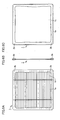
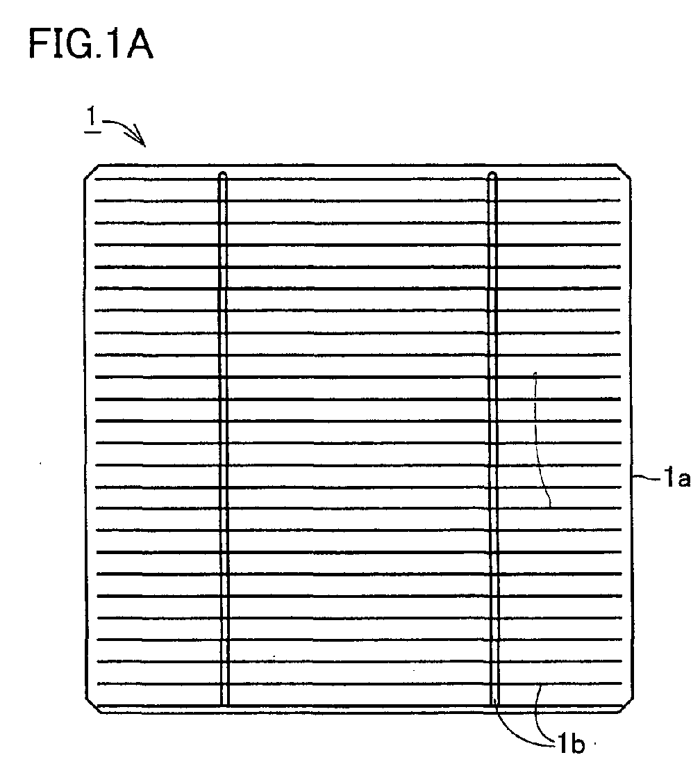
- a solar cell according to one embodiment of the present invention is schematically shown.
- Fig. 1A shows a front surface
- Fig. 1B shows a side surface
- Fig. 1C shows a back surface, of a solar cell 1.
- Solar cell 1 includes a silicon substrate 1a. Formed on the front surface of substrate 1a is a conventional comb-shaped silver electrode 1b for collecting current. The back surface of solar cell 1 is covered with a backside aluminum electrode 1c. A peripheral portion on the back surface of solar cell 1 is reinforced with resin 2.
- Solar cells usually have a thickness of about 350 ⁇ m.
- thinner solar cells have been desired in order to increase the number of cell substrates obtainable from an ingot for reducing cost.
- Cell fracture during production process has not been a serious problem for cell substrates having the thickness of about 350 ⁇ m.
- ratio of the fracture occurrence increases dramatically. As such, it is expected that the present invention is more effective particularly in thinner solar cells.
- the size of the solar cell's main surface is usually about 10cm square or larger. Cost reduction for the solar cell can be achieved also by making larger the dimension of the main surface thereof. In contrast, as the solar cell is made thinner and as the area of the main surface thereof is made larger, the solar cell is more likely to fracture.
- solar cell 1 is reinforced with resin 2 on the back surface thereof.
- resin 2 can be opaque and then an appropriate kind of reinforcing resin can be selected in view of its workability and cost.
- the harder the reinforcing material 2 is the larger load will be born by the reinforcing material. Therefore, hard material (having high elastic modulus) is desired for reinforcing material 2.
- the reinforcing material of harder property tends to easily achieve the effect of reinforcing even when it is made thin.
- reinforcing material 2 may be provided to a wider area on the back surface of solar cell 1 than shown in Fig. 1, or to the entire back surface.
- a back surface of a solar cell 1 in which a resin-reinforcing portion 2a is limited to vicinities of two sides opposing to each other on the back surface of the cell.
- a resin-reinforcing portion 2a is limited to vicinities of two sides opposing to each other on the back surface of the cell.
- opposing two sides of the cell are subject to external force in the production processes of the solar cell and the solar battery module.
- reinforcing the vicinity of the entire peripheral edge on the back surface of the cell as in Figs. 1A to 1C, therefore, by reinforcing the vicinities of only two sides readily subject to external force, a similar effect can be obtained.
- the reinforcing material provided to portions where the cell is in contact with a jig is expected to be effective as well.
- a material with higher elastic modulus for a reinforcing material is expected to contribute to higher effect of preventing cell fracture.
- addition of reinforcing fibers is particularly expected to enhance the effect.
- improvement in thermal resistance can also be expected, depending on a type of reinforcing fiber material to be added.
- a transparent reinforcing material 3 is provided in a vicinity of a peripheral edge on a front side of a solar cell 1.
- the reinforcing material such as transparent resin or glass can reinforce the front surface side, not limited to the back surface side of solar cell 1. It goes without saying that reinforcement on the back surface side of the cell as shown in Figs. 1A to 1C or Fig. 2 can be combined with that on the front surface side as shown in Fig. 3.
- Figs. 4A to 4C show a further embodiment.
- Fig. 4A shows a front surface
- Fig. 4B shows a side surface
- Fig. 4C shows a back surface, of a solar cell.
- a buffering material 4 is provided on the side surface side portion of a solar cell 1.
- buffering material 4 is provided on the side surface portion of solar cell 1
- damage to silicon substrate 1a due to concentration of external force to one point of the cell can be prevented in positioning or carrying the cell in the production process of the solar battery module. That is, use of a flexible material for buffering material 4 will serve to distribute the external force even if it is imposed on one point of solar cell 1.
- fracture of solar cell 1 will be less likely.
- Figs. 5A and 5B show a still further embodiment.
- Fig. 5A shows a back surface of a solar cell
- Fig. 5B shows an enlarged view of an encircled region 5B in Fig. 5A.
- a liquid reinforcing material 5a is introduced and then cure in a flaw or cracked portion 5 in a peripheral edge of solar cell 1, and thus the flaw or crack 5 is joined and reinforced.
- reinforcing material 5a is introduced in flaw or crack 5 for joint, the effect of reinforcement thereof is achieved by its adhesive strength, not by an influence of strength of reinforcing material 5a itself. Therefore, reinforcement is effective even if thickness of reinforcing material 5a is small, and thus the thickness itself is not significant.
- reinforcing material 5a in this example does not need to be thick, occurrence of thermal stress is almost negligible, which is due to a mismatch of thermal expansion coefficient of reinforcing material 5a itself relative to silicon or other materials constituting the solar battery module. Even if flaw or crack 5 is too small to be visually recognized, not the entire solar cell but such a weak portion can be selectively reinforced. This is achieved by utilizing the property of the liquid reinforcing material with wettability and surface tension to easily reach a small gap. For reinforcement in this application, therefore, reinforcing material 5a having properties of small viscosity, good fluidity, easy permeation to a small gap before curing and high adhesive strength can achieve the significant effect.
- Figs. 6A to 6C show a still further embodiment.
- Fig. 6A shows a front surface
- Fig. 6B shows a side surface
- Fig. 6C shows a back surface, of a solar cell.
- reinforcing material 2b is provided in vicinities of peripheral edge portions on both front and back sides of a solar cell 1. Therefore, warp of the cell will not be large even in an environment at a high or low temperature. That is, in the embodiment of Figs. 6A to 6C, warp of the cell due to the difference of thermal expansion coefficients between the solar cell and the reinforcing material can be made smaller than in the case of providing the reinforcing material on only either one of the front and back surfaces of the solar cell.
- a reinforcing material 2c is provided in vicinities of opposing two sides on a back surface of a solar cell 1.
- reinforcing material region 2c on the back surface of the cell is patterned so that thermal stress due to the difference of thermal expansion property between solar cell 1 and reinforcing material 2c can be made smaller.
- reinforcing material region 2c can be patterned so as to reduce the thermal stress without lowering the effect of reinforcing.
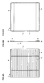
- Figs. 8A to 8C show a still further embodiment.
- Fig. 8A shows a front surface
- Fig. 8B shows a side surface
- Fig. 8C shows a back surface, of a solar cell.
- a solar cell 1 is reinforced by an aluminum plate, a ceramic plate or the like 6 joined with resin or the like 2d in vicinities of opposing two sides on the back surface of the cell.
- Such a reinforcing plate 6 may be joined slightly beyond the opposing two sides of solar cell 1. In this case, fracture of the cell can effectively be avoided by preventing the cell from directly abutting a jig during the production processes of the solar cell and the module.
- an effect of reinforcing the solar cell can be enhanced by further reinforcement with aluminum plate, ceramic plate or the like 6 in addition to reinforcement with resin 2d.
- the jig will directly abut not on cell substrate 1a but on reinforcing plate 6, for example in positioning cell 1 in the production process of the solar battery module.
- fracture of solar cell 1 can be reduced.
- conductive resin 2d and metal reinforcing plate 6 are used, an effect of lowering electrical resistance of the backside electrode of solar cell 1 can be obtained, and thus electrical output of the solar battery module can be improved.
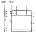
- Figs. 9A and 9B show a still furtherembodiment.
- Fig. 9A shows a side surface
- Fig. 9B show a back surface of a solar cell.
- a vicinity of each of opposing two sides on a back surface of a solar cell 1 is reinforced with a conductive resin 2e and a metal plate 7 joined thereto.
- metal plate 7 is a solderable reinforcing plate.
- adjacent cells are electrically connected by interconnectors 8. That is, interconnector 8 soldered to metal reinforcing plate 7 of one solar cell 1 is connected to a comb-shaped electrode on the front side of adjacent solar cell 1.
- connection portion of interconnector 8 made of copper band thermal stress due to the difference of thermal expansion coefficients between the copper band 8, solder 9 and silicon substrate 1a as well as thermal stress imposed to the connection portion due to the difference of thermal expansion coefficients between a material composing the solar battery module and the solar cell has caused fracture in the solar cell in some cases.
- conductive reinforcing materials 2e, 7 are used at the interconnector connection portion, such cell fracture can be prevented.
- a vicinity of a peripheral edge on a back surface of a solar cell 1 is reinforced with a silver electrode 10.
- An interconnector is connected to a connection region 10a in the silver electrode region 10 by soldering. Since silver electrode region 10 has small electrical resistance and can have the surface solder-plated, it is expected that resistance of the backside electrode can be effectively lowered and electrical property of the solar battery module can be simultaneously improved.
- the peripheral edge portion of a back surface of a solar cell is further reinforced by a metal reinforcing plate 11. That is, this metal reinforcing plate 11 is connected to silver electrode region 10 by soldering. It goes without saying that such a reinforcing plate may be provided to the entire back surface of solar cell 1.
- the interconnector since the interconnector is soldered to metal reinforcing plate 11, the solar cell substrate will not be subject to thermal stress due to soldering or load via the interconnector from a module constituting portion. Thus, damage to the cell can be reduced, and reliability thereof can be improved.
- a glass material is used for reinforcing material 2b in a similar case as in Figs. 6A to 6C.
- an n + region 1n and a p + region 1p are formed on a p-type silicon substrate 1a, and then a baked aluminum backside electrode 1c is formed on p + region 1p.
- pn junction is easily isolated at the peripheral edge portion of the wafer by providing glass reinforcing material 2b in a step prior to forming the pn junction and backside electrode 1c on silicon substrate 1a, and improvement in electrical output of solar cell 1 can be achieved.
- by introducing such reinforcing material 2b in an earlier step of the production process of solar cell 1 cell fracture during the cell production process can be reduced.
- An example of powdered glass which can be used for a source material of baked glass reinforcing material 2b is GP-5210, GP-1410 or the like from Nippon Electric Glass Co., Ltd.
- Figs. 13A and 13B show a still further embodiment.
- Fig. 13A shows a side surface and Fig. 13B shows a back surface of a solar cell.
- an aluminum plate 12 as a reinforcing plate is joined with a conductive adhesive 13 to the back surface side of the cell to cover almost entire area of baked aluminum electrode 1c.
- silver electrode 10b is formed by printing and baking silver paste, and solder coating 9a is provided thereon. Current flowing in baked aluminum electrode 1c and aluminum reinforcing plate 12 can be collected to silver electrode portions 10b where the interconnectors are to be soldered.
- Figs. 14A and 14B show a still further embodiment.
- Fig. 14A shows a side surface and Fig. 14B shows a back surface of a solar cell.
- a silver electrode 10 is formed by printing and baking silver paste on the peripheral portion of baked aluminum electrode 1c, and solder coating 9a is provided on silver electrode 10 by dipping.
- a steel plate is soldered to silver electrode 10 as a reinforcing plate 13, to which interconnectors 8 are connected with solder.
- the cell is reinforced not only with silver electrode 10 on the cell peripheral portion, but also with soldering reinforcing steel plate 13 to the cell by means of solder coating 9a on silver electrode 10. Since reinforcing steel plate 13 can serve also as an electrode, series resistance of the cell can be lowered and output thereof can be improved.
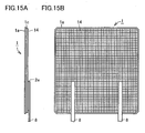
- Figs. 15A and 15B show a still further embodiment.
- Fig. 15A shows a side surface and Fig. 15B shows a back surface of a solar cell.
- aluminum paste 1c is printed on the back surface of the solar cell substrate, and before it is dried, an aluminum reinforcing plate 14 is bonded to aluminum paste 1c. Thereafter, by drying and baking aluminum paste 1c, aluminum reinforcing plate 14 is joined to cell substrate 1a. Further, using conductive resin 2e, interconnectors 8 are attached to aluminum reinforcing plate 14.
- mesh aluminum plate 14 is used. In this case, by sufficiently evaporating solvent component and burning resin component in the paste when drying and baking aluminum paste 1c, joint property between cell substrate 1a and aluminum reinforcing plate 14 can be improved significantly.
- Cell substrate 1a and reinforcing plate 14 may be welded together.
- thin aluminum plate 14 (as thick as about 200 ⁇ m) may be made in contact with a silicon surface on the back side of cell substrate 1a so as to directly join aluminum reinforcing plate 14 with the silicon surface by directing YAG (yttrium aluminum garnet) laser.
- YAG yttrium aluminum garnet
- Solar cells of which reinforcing material is non-conductive are preferred in terms of avoiding electrical contact between adjacent solar cells in a solar battery module. More specifically, it is usually designed to provide a gap of about 0.5 to 2mm between solar cells for preventing electrical contact between the cells. When it is difficult to precisely arrange solar cells in position, the cells can be arranged abutting each other, if a non-conductive reinforcing or buffering material is provided on the side surface of each solar cell. Then, it becomes easy to produce the solar battery module.
- Figs. 16A and 16B show a still further embodiment.
- Fig. 16A shows a back surface of a solar cell and
- Fig. 16B shows a cross-section taken along a line 16X - 16X in Fig. 16A.
- silicon wafers having an area of 125mm square and a thickness of 300 ⁇ m are used for substrates.
- a pattern 2f of baked silver is formed, which serves as the reinforcing material. Since the surface of the reinforcing material 2f of baked silver is coated with a solder layer 2e by dip soldering, solder layer 1e further reinforces reinforcing material 2f.
- reinforcing material 2f is formed with baked silver similarly as connection electrode 1d on the cell back surface, silver paste for them can simultaneously be printed and baked with screen process, and the effect of reinforcing the cell can be achieved without adding any process step.
- reinforcing material pattern 2f and backside connection electrode 1d were printed to a thickness of about 30 ⁇ m using silver paste and a screen of SUS 165 mesh.
- a pattern of baked silver was formed by baking silver paste print at about 600°C after drying at about 150°C. Thereafter, the surface of baked silver was coated with solder layer by dip soldering.
- reinforcing material pattern 2f was printed so as to overlay the peripheral edge portion of backside collector electrode 1c formed with baked aluminum.
- reinforcing material pattern 2f is of baked silver, in addition to the effect of reinforcing, an effect of lowering electrical resistance in a direction parallel to the back surface of silicon substrate 1a is also achieved. Therefore, when a plurality of cells are connected in series, output property (particularly, FF: fill factor) of the cells can be improved, compared with a conventional example.
- Fig. 17 is different in that reinforcing material pattern 2f is formed not only on the peripheral edge portion of backside collector electrode 1c but also overlaid on the peripheral edge portion of silicon substrate 1a. Since joint portion 3a between the baked silver reinforcing material pattern 2f and silicon wafer 1a has high joint strength, stronger reinforcement can be obtained effectively.
- width 3b of reinforcing material pattern 2f and aluminum collector electrode 1c is too large, separation is likely at an interface between baked silver 2f and baked aluminum 1c after dip soldering.
- width 3b was 8mm, separation was observed in 7 solar cells out of 10 at the interface between baked silver and baked aluminum.
- width 3b was 5mm separation was observed in 2 cells out of 10.
- width 3b was 4mm, separation was not observed in any cell.
- width 3b is desirably 4mm or smaller. In the present embodiment, the width was set to 1.5mm. Here, separation was not observed in any out of 100 solar cells produced for trial.
- a distance 3c from the peripheral edge of silicon wafer 1a to that of reinforcing material pattern 2f is too small, leakage current is liable to increase in the peripheral edge portion of solar cell 1.
- Leakage current Id of a conventional solar cell was about 0.1A while Id was increased to about 0.3A when distance 3c was set to 0.2mm.
- Id was about 0.1A similarly as in a conventional example. That is, in order to obtain the effect of reinforcing the cell without lowering electric property of the cell, distance 3c is desirably 0.5mm or larger. In the present embodiment, the distance was set to 1.0mm.
- a back surface of a solar cell according to a still further embodiment is shown, in which baked silver reinforcement portion 2f is limited to vicinities of two sides opposing each other on the cell back surface.
- baked silver reinforcement portion 2f is limited to vicinities of two sides opposing each other on the cell back surface.
- a cell edge portion is subject to large stress due to soldering of the interconnector made of metal having a thermal expansion coefficient considerably different from that of the solar cell. Therefore, cell fracture is liable to occur mainly along a direction of interconnector connection.
- sufficient reinforcement effect can be obtained even if only two sides where cell fracture is liable to occur are provided with reinforcing material 2f. In such a case, usage of expensive silver paste can be reduced, and reinforcement can be obtained with low cost.
- an interconnector is provided to the solar cell in Fig. 19A.
- an interconnector 8 is not only connected to backside connection electrode 1d, but also electrically connected to connection portion 4 of reinforcing material pattern 2f. Since baked silver reinforcing material pattern 2f can serve also as a collector electrode, output property (FF) of the cell can be improved by connecting interconnector 8 also to baked silver pattern 2f.
- a module was produced, in which reinforcing material pattern 2f and interconnector 8 are electrically connected by soldering, and 54 cells are serially connected.
- Table 1 shows comparisons of cell fracture ratios as well as output properties between the module of the present embodiment and the module produced with conventional solar cells.
- Isc represents a short circuit current of the module
- Voc represents an open-circuit voltage
- Pm represents a maximum output.
- FIG. 19B Although an embodiment shown in Fig. 19B is similar to that in Fig. 19A, width at portion 4 for connecting interconnector 8 to reinforcing material pattern 2f is made larger in Fig. 19B.
- FF output property
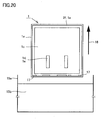
- Fig. 20 shows an example of dip soldering step for the solar cell of Fig. 16A.
- cell 1 is once immersed in molten solder 15b in a solder bath 15a, and then pulled up vertically as shown with an arrow 16.
- the cell provided with baked silver reinforcing material pattern 2f is liable to have solder accumulation 17 on reinforcing material 2 in a vicinity of the bottom side relative to the pull-up direction. If solder accumulation 17 is produced, cell fracture is more likely to occur originating therefrom. Solder accumulation 17 is produced because molten solder flows in large amount from the top to bottom along the pull-up direction.
- Figs. 21A to 21C show back surfaces of solar cells according to still further embodiments.
- one discontinuity 18a is provided in reinforcing material pattern 2f. Discontinuity 18a can retard solder flow into the bottom side of reinforcing material pattern 2f. Consequently, solder accumulation can be reduced.
- Fig. 21B two discontinuities 18b are provided at both end portions of the bottom side of reinforcing material pattern 2f. Accordingly, solder flow to the bottom side of reinforcing material pattern 2f can be made smaller, and solder accumulation is less likely to occur.
- Fig. 21C two discontinuities 18c are provided along diagonals of rectangular cell 1 at both end portions of the bottom side of reinforcing material pattern 2f.
- solder accumulation can further be effectively suppressed.
- Figs. 22A to 22C show other variations of discontinuities in reinforcing material pattern 2f.
- Fig. 23 show a back surface of a solar cell according to a still further embodiment.
- a comb-teeth pattern is provided in an area where solder accumulation tends to occur, so as to prevent solder accumulation.
- effect of lowering resistance as well as effect of reinforcing is not decreased.
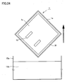
- Fig. 24 shows another example of a dip soldering step for the solar cell of Fig. 16A.
- Fig. 24 by pulling up rectangular cell 1 with the cell diagonally tilted, molten solder flow can be gathered at a corner thereof on any reinforcing material pattern. Since gathered solder is less likely to accumulate at the corner of the cell, solder accumulation on reinforcing material pattern 2f can be suppressed.
- occurrence of cell fracture due to external load can be decreased by reinforcing solar cell substrates.
- ratio of cell fracture in a production process of the solar cells can be lowered, and an availability factor of an apparatus for producing the cells can be improved.
- by suppressing cell fracture occurrence it becomes possible to reduce work for cleaning the production apparatus as well as cost for the solar cells and modules improving use efficiency of material.
- performance and reliability of the completed solar battery modules can be improved.
Landscapes
- Photovoltaic Devices (AREA)
Abstract
Description
| Isc [A] | Voc [V] | Pm [W] | FF | Ratio of Fracture | |
| Conventional Module | 5.36 | 32.7 | 125.3 | 0.715 | 6.2% |
| Present Embodiment | 5.32 | 32.6 | 125.7 | 0.725 | 3.4% |
Claims (29)
- A solar cell (1), having at least one of reinforcing material (2, 2a, 2b) and buffering material (2c) provided at least partially on at least one of a back surface, a front surface and a side surface of the solar cell.
- The solar cell according to claim 1, formed on a semiconductor substrate (1a) having a generally rectangular main surface with each side being at least 10cm and having a thickness of less than 350µm.
- The solar cell according to claim 1 or 2, wherein
one of said reinforcing material (2, 2a, 2b) and said buffering material (2c) includes at least one of glass, epoxy resin, acrylic resin, EVA resin, silicon resin, baked silver, glass fiber, carbon fiber, metal plate, ceramic plate and resin plate. - The solar cell according to any one of claims 1 to 3, wherein
said reinforcing material (2, 2a, 2b) is cured after injection into at least one of cracks, flaws and chips included in said cell (1). - The solar cell according to any one of claims 1 to 3, wherein
conductive said reinforcing material (2, 2a, 2b) is provided on the back surface of said cell (1), and an interconnector (8) for adjacent cells can be connected to the reinforcing material. - The solar cell according to any one of claims 1 to 3, wherein
said reinforcing material provided on the front surface side of said cell (1) is transparent (2b). - The solar cell according to any one of claims 1 to 3, wherein
said reinforcing material (2, 2a, 2b) or said buffering material (2c) is provided to a portion that contacts a jig for positioning and handling said cell (1) to be included in a solar battery module in a production process of the solar battery module. - The solar cell according to any one of claims 1 to 3, wherein
said reinforcing material (2, 2a, 2b) is patterned so as to reduce stress due to difference in thermal expansion coefficients between said reinforcing material and said semiconductor substrate (1a) as a temperature changes in an environment where said cell (1) is used. - The solar cell according to any one of claims 1 to 3, wherein
used for said reinforcing material (2, 2a, 2b) is a material of which quality does not alter even at a solder temperature in a dip soldering step of said cell (1). - The solar cell according to any one of claims 1 to 3, wherein
used for said reinforcing material (2b) is a glass material prepared by applying a solution including powdered glass dissolved in a solvent and volatilizing the solvent followed by baking is used. - A method of producing the solar cell (1) of claim 10, comprising the steps of baking the glass material for said reinforcing material and baking a backside aluminum electrode (1c) of said cell (1) to be carried out simultaneously.
- The solar cell according to any one of claims 1 to 3, wherein
formed on the front surface of said cell is a transparent reinforcing material having a thermal expansion coefficient comparable to that of the reinforcing material (2, 2a, 2b) provided on the back surface of said cell (1). - The solar cell according to any one of claims 1 to 3, wherein
said reinforcing material (2, 2a, 2b) includes a plate joined to said cell (1) by soldering or welding. - The solar cell according to any one of claims 1 to 3, wherein
said reinforcing material (2, 2a, 2b) includes at least one of an aluminum plate and a mesh aluminum plate, and said aluminum plate is joined to the back surface side of said cell with baked print aluminum paste. - A solar cell, having a reinforcing material (2, 2a) made of baked silver (2f) provided at least partially to a periphery of a back surface.
- The solar cell according to claim 15, wherein
a collector electrode on a front surface and a connection electrode on the back surface of the solar cell (1) are formed with baked silver (2f). - The solar cell according to claim 15 or 16, wherein
said collector electrode is formed except for a peripheral edge portion on the back surface of the solar cell (1), and the reinforcing material of said baked silver (2f) is formed on the peripheral edge portion of the collector electrode. - The solar cell according to claim 17, wherein
said reinforcing material (2, 2a, 2b) is formed extending also over the peripheral edge portion on the back surface of said cell. - The solar cell according to claim 15 or 16, wherein
said reinforcing material (2, 2a, 2b) is formed along vicinities of two sides intersecting a direction in which said cell (1) is connected by an interconnector (8). - The solar cell according to any one of claims 15 to 19, wherein
said reinforcing material (2, 2a, 2b) has a width of at most 4mm. - The solar cell according to any one of claims 15 to 20, wherein
said reinforcing material (2, 2a, 2b) is formed at least 0.5mm away from a peripheral edge of said cell (1). - The solar cell according to claim 16, wherein
said interconnector (8) is connected to both of said backside connection electrode 1d and said reinforcing material (2, 2a, 2b). - The solar cell according to claim 22, wherein
said reinforcing material (2, 2a, 2b) has a width made larger in a region where said interconnector (8) is connected. - The solar cell according to any one of claims 15 to 23, wherein
said reinforcing material (2, 2a, 2b) is not continuous along an entire periphery of the back surface of said cell (1), and is provided with at least one discontinuity. - The solar cell according to claim 24, wherein
said discontinuities of said reinforcing material (2, 2a, 2b) are provided at both end portions of one side of said cell (1). - The solar cell according to claim 24 or 25, wherein
said discontinuity of said reinforcing material (2, 2a, 2b) is formed diagonally, relative to one side of said cell (1). - The solar cell according to any one of claims 15 to 22, wherein
said reinforcing material (2, 2a, 2b) includes a comb-teeth pattern. - A method of producing a solar cell (1) according to claim 16, comprising the step of simultaneously forming said reinforcing material (2, 2a, 2b) and said backside connection electrode (1d).
- A method of producing the solar cell (1) of claim 16, comprising the step of pulling up said rectangular cell (1) in a direction approximately along its diagonal after dip soldering for coating said collector electrode on the front surface of said cell (1), said connection electrode (1d) on the back surface and said reinforcing material (2, 2a, 2b) with a solder layer.
Applications Claiming Priority (4)
| Application Number | Priority Date | Filing Date | Title |
|---|---|---|---|
| JP2001177995 | 2001-06-13 | ||
| JP2001177995 | 2001-06-13 | ||
| JP2001234817A JP2003069055A (en) | 2001-06-13 | 2001-08-02 | Solar cell and method of manufacturing the same |
| JP2001234817 | 2001-08-02 |
Publications (2)
| Publication Number | Publication Date |
|---|---|
| EP1267419A2 true EP1267419A2 (en) | 2002-12-18 |
| EP1267419A3 EP1267419A3 (en) | 2007-11-28 |
Family
ID=26616797
Family Applications (1)
| Application Number | Title | Priority Date | Filing Date |
|---|---|---|---|
| EP02013008A Withdrawn EP1267419A3 (en) | 2001-06-13 | 2002-06-12 | Solar cell and method of producing the same |
Country Status (3)
| Country | Link |
|---|---|
| US (1) | US7307210B2 (en) |
| EP (1) | EP1267419A3 (en) |
| JP (1) | JP2003069055A (en) |
Cited By (5)
| Publication number | Priority date | Publication date | Assignee | Title |
|---|---|---|---|---|
| WO2006133507A1 (en) * | 2005-06-17 | 2006-12-21 | The Australian National University | A solar cell interconnection process |
| WO2010051355A3 (en) * | 2008-10-31 | 2011-01-06 | Dow Corning Corporation | Photovoltaic cell module and method of forming |
| EP2403008A1 (en) * | 2010-07-01 | 2012-01-04 | Sika Technology AG | Cover sheet for solar cell |
| CN110534593A (en) * | 2019-08-30 | 2019-12-03 | 无锡携创新能源科技有限公司 | System of processing, processing method and the application method of dereliction grid cell piece copper mesh |
| CN115136402A (en) * | 2020-12-24 | 2022-09-30 | 宁德新能源科技有限公司 | Battery pack and electric device using same |
Families Citing this family (60)
| Publication number | Priority date | Publication date | Assignee | Title |
|---|---|---|---|---|
| JP2003069055A (en) | 2001-06-13 | 2003-03-07 | Sharp Corp | Solar cell and method of manufacturing the same |
| JP4074763B2 (en) * | 2002-01-22 | 2008-04-09 | シャープ株式会社 | Manufacturing method of solar cell |
| JP2004127987A (en) * | 2002-09-30 | 2004-04-22 | Sharp Corp | Solar cell and method of manufacturing the same |
| JP4675550B2 (en) * | 2003-04-28 | 2011-04-27 | 三菱マテリアル株式会社 | Unidirectionally solidified silicon ingot, method for producing the same, silicon plate and substrate for solar cell |
| JP4121928B2 (en) * | 2003-10-08 | 2008-07-23 | シャープ株式会社 | Manufacturing method of solar cell |
| JP2005136125A (en) * | 2003-10-30 | 2005-05-26 | Kyocera Corp | Photoelectric conversion device |
| KR101087202B1 (en) * | 2003-11-27 | 2011-11-29 | 쿄세라 코포레이션 | Solar modules |
| US20050268963A1 (en) * | 2004-02-24 | 2005-12-08 | David Jordan | Process for manufacturing photovoltaic cells |
| WO2007043428A1 (en) * | 2005-10-14 | 2007-04-19 | Sharp Kabushiki Kaisha | Solar cell, solar cell provided with interconnector, solar cell string and solar cell module |
| EP1947703B1 (en) * | 2005-10-14 | 2019-08-14 | Sharp Kabushiki Kaisha | Interconnector, solar battery string using such interconnector |
| JP4986462B2 (en) * | 2006-01-27 | 2012-07-25 | シャープ株式会社 | SOLAR CELL STRING, MANUFACTURING METHOD THEREOF, AND SOLAR CELL MODULE USING THE SOLAR CELL STRING |
| JP5084146B2 (en) * | 2006-01-30 | 2012-11-28 | 三洋電機株式会社 | Photovoltaic module |
| US8440907B2 (en) | 2006-04-14 | 2013-05-14 | Sharp Kabushiki Kaisha | Solar cell, solar cell string and solar cell module |
| JPWO2009107804A1 (en) * | 2008-02-28 | 2011-07-07 | 三洋電機株式会社 | Solar cell module |
| TWI382544B (en) * | 2008-09-16 | 2013-01-11 | Nexpower Technology Corp | Optical solar module |
| JP5362379B2 (en) * | 2009-02-06 | 2013-12-11 | 三洋電機株式会社 | Method for measuring IV characteristics of solar cell |
| US9012766B2 (en) | 2009-11-12 | 2015-04-21 | Silevo, Inc. | Aluminum grid as backside conductor on epitaxial silicon thin film solar cells |
| US9214576B2 (en) | 2010-06-09 | 2015-12-15 | Solarcity Corporation | Transparent conducting oxide for photovoltaic devices |
| US9773928B2 (en) | 2010-09-10 | 2017-09-26 | Tesla, Inc. | Solar cell with electroplated metal grid |
| EP2617065A2 (en) * | 2010-09-17 | 2013-07-24 | Dow Global Technologies LLC | Improved photovoltaic cell assembly and method |
| US9800053B2 (en) | 2010-10-08 | 2017-10-24 | Tesla, Inc. | Solar panels with integrated cell-level MPPT devices |
| WO2012124464A1 (en) * | 2011-03-16 | 2012-09-20 | 三洋電機株式会社 | Solar cell |
| US9054256B2 (en) | 2011-06-02 | 2015-06-09 | Solarcity Corporation | Tunneling-junction solar cell with copper grid for concentrated photovoltaic application |
| WO2013140552A1 (en) * | 2012-03-21 | 2013-09-26 | 三洋電機株式会社 | Solar cell module |
| CN102825933B (en) * | 2012-09-13 | 2014-12-24 | 英利能源(中国)有限公司 | Screen printing method for solar cell, solar cell and preparation method for solar cell |
| EP2904643B1 (en) | 2012-10-04 | 2018-12-05 | SolarCity Corporation | Solar cell with electroplated metal grid |
| US9865754B2 (en) | 2012-10-10 | 2018-01-09 | Tesla, Inc. | Hole collectors for silicon photovoltaic cells |
| US20140124014A1 (en) | 2012-11-08 | 2014-05-08 | Cogenra Solar, Inc. | High efficiency configuration for solar cell string |
| US9281436B2 (en) | 2012-12-28 | 2016-03-08 | Solarcity Corporation | Radio-frequency sputtering system with rotary target for fabricating solar cells |
| US10074755B2 (en) | 2013-01-11 | 2018-09-11 | Tesla, Inc. | High efficiency solar panel |
| US9412884B2 (en) | 2013-01-11 | 2016-08-09 | Solarcity Corporation | Module fabrication of solar cells with low resistivity electrodes |
| US9219174B2 (en) | 2013-01-11 | 2015-12-22 | Solarcity Corporation | Module fabrication of solar cells with low resistivity electrodes |
| US9624595B2 (en) | 2013-05-24 | 2017-04-18 | Solarcity Corporation | Electroplating apparatus with improved throughput |
| US9608140B2 (en) * | 2013-10-30 | 2017-03-28 | Kyocera Corporation | Solar cell and solar cell module |
| KR101550978B1 (en) | 2013-11-18 | 2015-09-07 | 현대자동차주식회사 | A method for manufacturing a solar cell that compensation patterns for preventing warp defectiveness are inserted |
| CN103746012A (en) * | 2014-01-02 | 2014-04-23 | 杭州塞利仕科技有限公司 | Manufacturing technology for solar cell positive electrodes |
| KR102271055B1 (en) * | 2014-06-26 | 2021-07-01 | 엘지전자 주식회사 | Solar cell module |
| US10309012B2 (en) | 2014-07-03 | 2019-06-04 | Tesla, Inc. | Wafer carrier for reducing contamination from carbon particles and outgassing |
| US10056522B2 (en) | 2014-12-05 | 2018-08-21 | Solarcity Corporation | System and apparatus for precision automation of tab attachment for fabrications of solar panels |
| US9590132B2 (en) | 2014-12-05 | 2017-03-07 | Solarcity Corporation | Systems and methods for cascading photovoltaic structures |
| US9991412B2 (en) | 2014-12-05 | 2018-06-05 | Solarcity Corporation | Systems for precision application of conductive adhesive paste on photovoltaic structures |
| US9899546B2 (en) | 2014-12-05 | 2018-02-20 | Tesla, Inc. | Photovoltaic cells with electrodes adapted to house conductive paste |
| US10236406B2 (en) | 2014-12-05 | 2019-03-19 | Solarcity Corporation | Systems and methods for targeted annealing of photovoltaic structures |
| US10043937B2 (en) | 2014-12-05 | 2018-08-07 | Solarcity Corporation | Systems and method for precision automated placement of backsheet on PV modules |
| US9685579B2 (en) | 2014-12-05 | 2017-06-20 | Solarcity Corporation | Photovoltaic structure cleaving system |
| US9947822B2 (en) | 2015-02-02 | 2018-04-17 | Tesla, Inc. | Bifacial photovoltaic module using heterojunction solar cells |
| US9955802B2 (en) | 2015-04-08 | 2018-05-01 | Fasteners For Retail, Inc. | Divider with selectively securable track assembly |
| US9761744B2 (en) | 2015-10-22 | 2017-09-12 | Tesla, Inc. | System and method for manufacturing photovoltaic structures with a metal seed layer |
| US9842956B2 (en) | 2015-12-21 | 2017-12-12 | Tesla, Inc. | System and method for mass-production of high-efficiency photovoltaic structures |
| US9496429B1 (en) | 2015-12-30 | 2016-11-15 | Solarcity Corporation | System and method for tin plating metal electrodes |
| US10115838B2 (en) | 2016-04-19 | 2018-10-30 | Tesla, Inc. | Photovoltaic structures with interlocking busbars |
| CN109463014A (en) * | 2016-06-28 | 2019-03-12 | 京瓷株式会社 | Solar cell module |
| KR101879374B1 (en) * | 2017-02-22 | 2018-08-17 | 주식회사 탑선 | Solar cell module |
| USD841570S1 (en) * | 2017-08-25 | 2019-02-26 | Flex Ltd | Solar cell |
| US10672919B2 (en) | 2017-09-19 | 2020-06-02 | Tesla, Inc. | Moisture-resistant solar cells for solar roof tiles |
| USD855016S1 (en) * | 2017-10-24 | 2019-07-30 | Flex Ltd. | Solar cell |
| USD855017S1 (en) * | 2017-10-24 | 2019-07-30 | Flex Ltd. | Solar cell |
| CN109788643B (en) * | 2017-11-10 | 2024-07-30 | 泰连公司 | Aluminum-based weldable contacts |
| US11190128B2 (en) | 2018-02-27 | 2021-11-30 | Tesla, Inc. | Parallel-connected solar roof tile modules |
| KR102001230B1 (en) * | 2018-06-28 | 2019-07-17 | 주식회사 탑선 | Solar cell module |
Family Cites Families (30)
| Publication number | Priority date | Publication date | Assignee | Title |
|---|---|---|---|---|
| US4132570A (en) * | 1977-08-24 | 1979-01-02 | Exxon Research & Engineering Co. | Structural support for solar cell array |
| US4287382A (en) * | 1980-05-09 | 1981-09-01 | Exxon Research & Engineering Co. | Solar cell assembly and fabrication of solar cell panels utilizing same |
| JPS61108178A (en) * | 1984-11-01 | 1986-05-26 | Nec Corp | solar cell module |
| JPS61268428A (en) | 1985-05-22 | 1986-11-27 | Chiku Asano | Shaping of plastic and composite material therefor |
| JPS6249672A (en) * | 1985-08-29 | 1987-03-04 | Sumitomo Electric Ind Ltd | Amorphous photovoltaic device |
| JPS6351152A (en) | 1986-08-21 | 1988-03-04 | Matsushita Electric Ind Co Ltd | Electrode head |
| US5100808A (en) * | 1990-08-15 | 1992-03-31 | Spectrolab, Inc. | Method of fabricating solar cell with integrated interconnect |
| US5118362A (en) * | 1990-09-24 | 1992-06-02 | Mobil Solar Energy Corporation | Electrical contacts and methods of manufacturing same |
| JP2641794B2 (en) * | 1990-09-28 | 1997-08-20 | シャープ株式会社 | Method of manufacturing solar cell module |
| US5273911A (en) * | 1991-03-07 | 1993-12-28 | Mitsubishi Denki Kabushiki Kaisha | Method of producing a thin-film solar cell |
| JP2758749B2 (en) | 1991-10-17 | 1998-05-28 | シャープ株式会社 | Photoelectric conversion device and method of manufacturing the same |
| US5320684A (en) * | 1992-05-27 | 1994-06-14 | Mobil Solar Energy Corporation | Solar cell and method of making same |
| JP2686022B2 (en) * | 1992-07-01 | 1997-12-08 | キヤノン株式会社 | Method for manufacturing photovoltaic element |
| JP3131549B2 (en) | 1994-12-29 | 2001-02-05 | 京セラ株式会社 | Solar cell module and method of manufacturing the same |
| JPH0951118A (en) | 1995-08-09 | 1997-02-18 | Shiroki Corp | Sheet solar cell |
| JPH10247629A (en) | 1997-03-04 | 1998-09-14 | M Setetsuku Kk | Semiconductor wafer manufacturing method, semiconductor wafer, and solar cell using this semiconductor wafer |
| JPH1150607A (en) * | 1997-08-05 | 1999-02-23 | Asahi Chem Ind Co Ltd | Waterproof sheet integrally formed with solar cell |
| JPH11156885A (en) * | 1997-11-27 | 1999-06-15 | Sekisui Chem Co Ltd | Method of manufacturing solar cell module |
| JP3577430B2 (en) | 1999-06-09 | 2004-10-13 | シャープ株式会社 | Solar cell and method of manufacturing the same |
| AU767581B2 (en) | 1999-08-25 | 2003-11-20 | Kaneka Corporation | Thin film photoelectric conversion module and method of manufacturing the same |
| JP2001202822A (en) | 2000-01-21 | 2001-07-27 | Murata Mfg Co Ltd | Conductive paste |
| JP3649393B2 (en) * | 2000-09-28 | 2005-05-18 | シャープ株式会社 | Silicon wafer processing method, silicon wafer and silicon block |
| US6787692B2 (en) | 2000-10-31 | 2004-09-07 | National Institute Of Advanced Industrial Science & Technology | Solar cell substrate, thin-film solar cell, and multi-junction thin-film solar cell |
| JP3753605B2 (en) | 2000-11-01 | 2006-03-08 | シャープ株式会社 | Solar cell and method for manufacturing the same |
| JP2002217434A (en) * | 2001-01-19 | 2002-08-02 | Sharp Corp | Solar cells, interconnectors and strings for solar cells |
| JP2003069055A (en) | 2001-06-13 | 2003-03-07 | Sharp Corp | Solar cell and method of manufacturing the same |
| JP3910072B2 (en) * | 2002-01-30 | 2007-04-25 | 東洋アルミニウム株式会社 | Paste composition and solar cell using the same |
| JP2004127987A (en) | 2002-09-30 | 2004-04-22 | Sharp Corp | Solar cell and method of manufacturing the same |
| JP2004179618A (en) * | 2002-10-04 | 2004-06-24 | Sharp Corp | SOLAR CELL, ITS MANUFACTURING METHOD, SOLAR CELL INTERCONNECTOR, STRING AND MODULE |
| JP2004146464A (en) * | 2002-10-22 | 2004-05-20 | Sharp Corp | SOLAR CELL, ITS MANUFACTURING METHOD, SOLAR CELL INTERCONNECTOR, STRING AND MODULE |
-
2001
- 2001-08-02 JP JP2001234817A patent/JP2003069055A/en active Pending
-
2002
- 2002-06-12 EP EP02013008A patent/EP1267419A3/en not_active Withdrawn
- 2002-06-13 US US10/167,649 patent/US7307210B2/en not_active Expired - Fee Related
Cited By (13)
| Publication number | Priority date | Publication date | Assignee | Title |
|---|---|---|---|---|
| WO2006133507A1 (en) * | 2005-06-17 | 2006-12-21 | The Australian National University | A solar cell interconnection process |
| CN101228638B (en) * | 2005-06-17 | 2010-09-08 | 澳大利亚国立大学 | Solar cell interconnection process |
| EP2485277A3 (en) * | 2008-10-31 | 2012-09-26 | Dow Corning Corporation | Photovoltaic cell module and method of forming |
| CN102272947A (en) * | 2008-10-31 | 2011-12-07 | 陶氏康宁公司 | Photovoltaic cell assembly and method of forming |
| WO2010051355A3 (en) * | 2008-10-31 | 2011-01-06 | Dow Corning Corporation | Photovoltaic cell module and method of forming |
| EP2485276A3 (en) * | 2008-10-31 | 2012-09-26 | Dow Corning Corporation | Photovoltaic Cell Module and Method of Forming |
| TWI508317B (en) * | 2008-10-31 | 2015-11-11 | Dow Corning | Photovoltaic battery module and forming method |
| US9842952B2 (en) | 2008-10-31 | 2017-12-12 | Dow Corning Corporation | Photovoltaic cell module and method of forming |
| EP2403008A1 (en) * | 2010-07-01 | 2012-01-04 | Sika Technology AG | Cover sheet for solar cell |
| WO2012001165A3 (en) * | 2010-07-01 | 2012-07-05 | Sika Technology Ag | Covering layer for solar cell |
| CN110534593A (en) * | 2019-08-30 | 2019-12-03 | 无锡携创新能源科技有限公司 | System of processing, processing method and the application method of dereliction grid cell piece copper mesh |
| CN115136402A (en) * | 2020-12-24 | 2022-09-30 | 宁德新能源科技有限公司 | Battery pack and electric device using same |
| CN115136402B (en) * | 2020-12-24 | 2023-12-05 | 宁德新能源科技有限公司 | Battery pack and power utilization device applying same |
Also Published As
| Publication number | Publication date |
|---|---|
| EP1267419A3 (en) | 2007-11-28 |
| US7307210B2 (en) | 2007-12-11 |
| US20030000571A1 (en) | 2003-01-02 |
| JP2003069055A (en) | 2003-03-07 |
Similar Documents
| Publication | Publication Date | Title |
|---|---|---|
| US7307210B2 (en) | Solar cell and method of producing the same | |
| EP2020688B1 (en) | Solar cell interconnection using thermo-compression bonding and correspondingly fabricated module | |
| CN101939847B (en) | Solar cell module and solar cell | |
| US8916038B2 (en) | Free-standing metallic article for semiconductors | |
| US8691694B2 (en) | Solderless back contact solar cell module assembly process | |
| US20140124027A1 (en) | Solar cell and method of manufacturing a solar cell | |
| CN102132419B (en) | Photoelectric conversion cell and photoelectric conversion module | |
| JPWO2013069425A1 (en) | Solar cell module and manufacturing method thereof | |
| CN102272938B (en) | Photoelectric conversion cell, photoelectric conversion module, and method for manufacturing photoelectric conversion cell | |
| JP5126878B2 (en) | Solar cell manufacturing method and solar cell | |
| CN121057337A (en) | A photovoltaic module and its printing process | |
| JP5436697B2 (en) | Solar cell module and manufacturing method thereof | |
| CN101088167B (en) | Solar cell unit | |
| JP4299772B2 (en) | Solar cell module | |
| JP4780953B2 (en) | Solar cell element and solar cell module using the same | |
| JP2009272406A (en) | Solar battery element | |
| JP2008288278A (en) | Manufacturing method of solar cell module | |
| JP4753816B2 (en) | Solar cell and manufacturing method thereof | |
| JP2002353475A (en) | Solar cell element | |
| JP5196418B2 (en) | Solar cell and solar cell module with interconnector | |
| JP2004128411A (en) | Solar cell and method of manufacturing the same | |
| JP4215500B2 (en) | Manufacturing method of solar cell | |
| KR20190043291A (en) | Solar cell module using divided cell and conductive foil | |
| HK1148608A (en) | Solar cell | |
| HK1111807B (en) | Solar cell |
Legal Events
| Date | Code | Title | Description |
|---|---|---|---|
| PUAI | Public reference made under article 153(3) epc to a published international application that has entered the european phase |
Free format text: ORIGINAL CODE: 0009012 |
|
| AK | Designated contracting states |
Kind code of ref document: A2 Designated state(s): AT BE CH CY DE DK ES FI FR GB GR IE IT LI LU MC NL PT SE TR |
|
| AX | Request for extension of the european patent |
Free format text: AL;LT;LV;MK;RO;SI |
|
| PUAL | Search report despatched |
Free format text: ORIGINAL CODE: 0009013 |
|
| AK | Designated contracting states |
Kind code of ref document: A3 Designated state(s): AT BE CH CY DE DK ES FI FR GB GR IE IT LI LU MC NL PT SE TR |
|
| AX | Request for extension of the european patent |
Extension state: AL LT LV MK RO SI |
|
| AKX | Designation fees paid | ||
| STAA | Information on the status of an ep patent application or granted ep patent |
Free format text: STATUS: THE APPLICATION IS DEEMED TO BE WITHDRAWN |
|
| 18D | Application deemed to be withdrawn |
Effective date: 20080529 |
|
| REG | Reference to a national code |
Ref country code: DE Ref legal event code: 8566 |