EP1263215A2 - Control of flashlight in a digital camera - Google Patents
Control of flashlight in a digital camera Download PDFInfo
- Publication number
- EP1263215A2 EP1263215A2 EP02396077A EP02396077A EP1263215A2 EP 1263215 A2 EP1263215 A2 EP 1263215A2 EP 02396077 A EP02396077 A EP 02396077A EP 02396077 A EP02396077 A EP 02396077A EP 1263215 A2 EP1263215 A2 EP 1263215A2
- Authority
- EP
- European Patent Office
- Prior art keywords
- flashlight
- image
- time
- exposure
- flash
- Prior art date
- Legal status (The legal status is an assumption and is not a legal conclusion. Google has not performed a legal analysis and makes no representation as to the accuracy of the status listed.)
- Granted
Links
- 230000010354 integration Effects 0.000 claims abstract description 26
- 238000000034 method Methods 0.000 claims abstract description 21
- 238000005096 rolling process Methods 0.000 claims abstract description 9
- 230000001960 triggered effect Effects 0.000 claims abstract description 5
- 238000012545 processing Methods 0.000 claims description 28
- 239000011159 matrix material Substances 0.000 claims description 20
- 238000012805 post-processing Methods 0.000 claims description 8
- 238000005516 engineering process Methods 0.000 claims description 3
- 238000003384 imaging method Methods 0.000 description 5
- 230000000694 effects Effects 0.000 description 4
- 238000010891 electric arc Methods 0.000 description 4
- 239000003990 capacitor Substances 0.000 description 3
- 238000003672 processing method Methods 0.000 description 3
- 238000006243 chemical reaction Methods 0.000 description 2
- 238000004146 energy storage Methods 0.000 description 2
- 238000005286 illumination Methods 0.000 description 2
- 239000004065 semiconductor Substances 0.000 description 2
- 238000003860 storage Methods 0.000 description 2
- 230000001360 synchronised effect Effects 0.000 description 2
- 239000003086 colorant Substances 0.000 description 1
- 230000000295 complement effect Effects 0.000 description 1
- 230000003111 delayed effect Effects 0.000 description 1
- 230000001419 dependent effect Effects 0.000 description 1
- 230000001771 impaired effect Effects 0.000 description 1
- 238000004519 manufacturing process Methods 0.000 description 1
- 229910044991 metal oxide Inorganic materials 0.000 description 1
- 150000004706 metal oxides Chemical class 0.000 description 1
- 229920006395 saturated elastomer Polymers 0.000 description 1
- 238000001228 spectrum Methods 0.000 description 1
Images


Classifications
-
- H—ELECTRICITY
- H04—ELECTRIC COMMUNICATION TECHNIQUE
- H04N—PICTORIAL COMMUNICATION, e.g. TELEVISION
- H04N23/00—Cameras or camera modules comprising electronic image sensors; Control thereof
- H04N23/70—Circuitry for compensating brightness variation in the scene
- H04N23/74—Circuitry for compensating brightness variation in the scene by influencing the scene brightness using illuminating means
-
- H—ELECTRICITY
- H04—ELECTRIC COMMUNICATION TECHNIQUE
- H04N—PICTORIAL COMMUNICATION, e.g. TELEVISION
- H04N25/00—Circuitry of solid-state image sensors [SSIS]; Control thereof
- H04N25/50—Control of the SSIS exposure
- H04N25/53—Control of the integration time
- H04N25/531—Control of the integration time by controlling rolling shutters in CMOS SSIS
Definitions
- the invention relates to a method for controlling the operation of a flashlight in connection with an electronic image sensor operating without a separate external shutter, as set forth in the preamble of the appended claim 1.
- Digital image sensors based on semiconductor technology such as matrix sensors based on charge coupled devices (CCD) and complementary metal oxide semiconductor (CMOS) technology, now make it possible to provide a large variety of devices with built-in imaging functions.
- image sensors are used e.g. in digital video and still cameras intended for consumers, as well as in various camera devices connected to computers, such as so-called network cameras. Thanks to their high degree of integration, compact size and low power consumption, particularly CMOS sensors are also very suitable for use in small-size portable devices, such as mobile stations and so-called personal data assistants (PDA).
- PDA personal data assistants
- a digital camera i.e . a digital image sensor
- a digital image sensor is implemented in a device which is small in size (portable) and/or inexpensive in its sale price
- One way to simplify the structure of the digital camera is to eliminate a separate, typically mechanically operated shutter which is used in front of the sensor matrix to control the exposure time.
- the exposure time is controlled electronically by controlling the functions of the sensor matrix.
- the CMOS image sensor consists of a matrix of photosensitive pixels.
- the pixel When light strikes a single pixel, the pixel is charged with an electric charge which is proportional to the amount of incoming light and is further stored in or in connection with said pixel.
- the charge is converted by means of a charge amplifier to a voltage which is further conducted via an analog-to-digital (AD) conversion out of the image sensor.
- AD analog-to-digital
- the exposure time of a single pixel in the CMOS sensor consists of the time during which the pixel is allowed to integrate the electric charge formed by this incoming light.
- the integration or exposure time starts at the point of time when the previous charge contained in the pixel is first adjusted to zero by a reset function, and ends when the pixel charge is read by a sample function.
- the solution commonly used is to process a CMOS matrix sensor row by row, i.e . to perform the operations of resetting, integration and reading for one pixel row of the matrix at a time.
- This makes the sensor structure considerably simpler, and thus also the transfer of the image information out of the sensor circuit will take place naturally in serial form, row by row, wherein the requirements set for the image information transfer rate are easier.
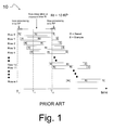
- Figure 1 shows, in principle, the row-by-row processing of the image sensor and its effect on the exposure of the different rows of the sensor.
- the rows are reset one by one with a reset function (R).
- R reset function
- the resetting (R) of successive rows takes place at the same rate at which the rows will be read with the sample function (S) at a later stage.
- the period of time between the resetting operations (R) of two successive rows is called row processing time (RP).
- the minimum value for the row processing time (RP) is determined by the rate at which the sensor circuit can transfer image information out of the circuit. Consequently, the row processing time (RP) also indicates the time which is taken between the sample operations (S) of two successive rows.
- the row integration or exposure time (RI) can now be formed of suitable multiples of the row processing time (RP) in such a way that the exposure time (RI) is kept equal for all the rows.
- the time selected for the exposure time is 10 ⁇ the processing time (RP).
- the exposure/integration times (RI) of adjacent rows of the image sensor, to be processed one after the other, are partly overlapping, but the exposure/integration takes place clearly at different times in rows which are far from each other, for example at the upper and lower edges of the sensor.
- Row-by-row processing of the image area in the above-described manner is known from prior art as a rolling electronic shutter or as a rolling window shutter.
- the rolling electronic shutter will not cause considerable harm to the imaging and to the image quality.
- the duration of a flash in flashlights based on a discharge tube, used in pocket cameras or the like typically varies from some tens of microseconds to some hundreds of microseconds.
- the processing of the whole image area typically takes several tens of milliseconds when a rolling electronic shutter is used.
- the flash of the flashlight is considerably shorter than the processing of the whole image area, this will cause that different rows of the sensor will be exposed in significantly different ways when the flashlight is used, and therefore, the quality of the images taken with the flashlight is impaired.
- the method according to the invention is primarily characterized in what will be presented in the characterizing part of the independent claim 1.
- the invention is based on the idea that during the time required for exposing one image, several separate, successive light flashes are used instead of a single light flash, to balance the exposure of different sub-areas of the image sensor to be processed at different times and thus integrating the charge at different times.
- the basic idea of the invention is that the flashes of the flash unit to be used for a single image are timed so that each single flash of the flash unit is performed at a point of time which is common to the integration or exposure time (RI) of as many successive sub-areas of the sensor as possible, such as rows, to be exposed at a time. Further, the successive flashes are also timed so that one and only one light flash occurs during the exposure time of each said sub-area.
- the significant advantage is attained by the present invention that it minimizes the number of light flashes required for one image while it also secures that the object to be imaged is illuminated as evenly as possible during the exposure (RI) of each sub-area of the sensor.
- the minimization of the number of light flashes is very important particularly in portable and/or other battery-operated devices in which the total power consumption of the flash should be kept as low as possible to save the capacity of the batteries and/or to minimize their size.
- the invention effectively prevents blurring of the image caused by the movement of the object, in a way to be described more closely hereinbelow.
- the number of flashes required for one image is determined by means of the ratio between the row processing time (RP) of the matrix sensor and the integration or exposure time (RI) used in the shooting.
- the ratio RI/RP indicates the number of successive rows which can be covered by one flash of the flash unit.
- the flashlight control according to the invention can be used in normal camera shooting with a flashlight under dark or dim conditions, or also in producing a fill-in flash under illuminated conditions.
- the invention can also be applied in the storage of so-called super resolution images.
- super resolution images several successive images in which the object is slightly transferred with respect to the image area are combined by means of image processing into a single new image.
- the resolution of the combined image is better than the pixel resolution of the original images.
- the invention is preferably applied particularly in connection with CMOS image sensors, to produce a simple, compact digital camera with a low power consumption.
- CMOS image sensors Such a digital camera is suitable to be placed e.g. in a mobile station or in another corresponding portable personal device.
- the invention is primarily described in connection with a matrix sensor to be exposed and read in pixel rows, it can also be used in connection with sensors to be processed in columns or in sub-areas in another way.
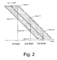
- Figure 2 shows, in principle, how the flashes of a flashlight of the invention are timed in connection with a matrix sensor to be processed and exposed row by row according to Fig. 1 or in a way substantially corresponding to Fig. 1.
- the start of the integration or exposure time (RI) of each pixel row in the sensor is delayed from the start of the exposure time (RI) of the preceding row by the time of the reset function (R), i.e. by the row processing time (RP). For this reason, the exposure times of successive rows are shifted with respect to each other as shown in Fig. 2.
- the flashes of the flashlight to be used for one image are timed in such a way that each single flash of the flashlight is triggered at a point of time which is common to the integration or exposure time (RI) of as many successive rows as possible.
- the first flash is thus timed to the point of time marked with the first vertical line, wherein the flash affects the exposure of the rows 0 to 11, but not the exposure of the other rows of the sensor.
- the next flash of the flashlight is timed to the point of the time marked with the second vertical line, wherein the second flash only affects the exposure of the rows 12 to 23.
- the second flash does not affect the exposure of the preceding rows 0 to 11 nor the exposure of the following rows, starting from the row 24.
- the third flash only exposes the rows 24 to 31.
- successive flashes are thus timed so that there is one and only one light flash during the exposure time of each pixel row 0 to 31. This is important so that the quantity of light produced by the flash at each pixel row remains substantially equal. At the same time, the minimum number of flashes required for the exposure of one image is determined, wherein the total power consumption of the flash is also minimized.
- each pixel in a single pixel row starts simultaneously after the reset function (R) to be performed for said row and ends simultaneously in the reading of the pixel values by the sample function (S). Consequently, with respect to the quantity of light received by the pixels in a single pixel row, it is not significant at which point of the integration or exposure time (RI) of said pixel row the flash occurs.
- the number of flashes required per one image is determined by means of the ratio between the row processing time (RP) of the matrix sensor and the integration or exposure time (RI) used in the shooting.
- Said ratio RI/RP indicates the number of successive rows in the matrix sensor which can always be covered by one pulse of the flashlight.
- 12 successive rows can always be covered by means of one pulse.
- RI 10 RP, wherein it would always be possible to cover 10 rows at a time by means of one flashlight pulse.
- the exposure time (RI) can be selected to be relatively long, because under these conditions, there is no significant light other than the flashlight coming into the camera sensor.
- one light flash can be used to cover several pixel rows of the sensor at a time; that is, fewer flashes are required for the whole image area.
- the exposure time (RI) is selected to be shorter to prevent overexposure of the pixel rows because of the prevailing light.
- the RI/RP ratio is reduced, the number of flashes required to expose the whole image area will increase.
- Fig. 3 shows the behaviour of the light flash (intensity of the light pulse) of a commercially available pocket-type digital camera (Canon QV-770) as a function of time.
- the graph of Fig. 3 can be considered to represent the typical operation of a flashlight based on the use of a flash tube built in a pocket-type camera or the like, the flashlight having a sufficient output capacity to be used in connection with conventional matrix sensors, such as CMOS sensors, under normal shooting conditions.
- each square interval of the horizontal axis represents a time interval of 100 microseconds
- the vertical axis represents the intensity of the light flash in a relative linear scale.
- Figure 3 indicates that the duration of the intensity maximum of said light flash is in the order of a few hundred microseconds.
- CMOS sensor with VGA resolution 640 ⁇ 480 pixels
- the processing of the whole image area typically takes several tens milliseconds.
- the row processing time can be e.g. about 3500 clock cycles, which corresponds to 140 microseconds if the clock cycle is 40 nanoseconds.
- the processing of the whole image, i.e . 480 rows, will thus take 67.2 milliseconds.
- the principle is that all the pixel rows of the image sensor are set to zero by a quick reset function to start the integration time (INT) for all the rows as simultaneously as possible.
- an external mechanical shutter is opened at a point of time T on to start the exposure of all the rows simultaneously.
- T off the external shutter is closed, correspondingly, to terminate the exposure of all the rows simultaneously.
- the exposure time for each sensor row thus becomes the open time T off -T on of the external shutter.
- the pixel rows can be read by a sample operation at a rate which is limited by the rate of transfer of image information from said sensor circuit and which rate of transfer is thus typically significantly slower than said quick reset function.
- INT integration times
- said shutter mode of the sensor can be used in a known manner in connection with a flashlight also without a separate external shutter in the following way.
- the flash of the flashlight illuminating the object is placed in the same way as if there were a separate external shutter used in the camera. If the light entering the sensor primarily originates from the flash only, all the rows of the sensor will be uniformly exposed even if there is no external shutter in use. However, if there is also other ambient light coming into the sensor, the last rows of the sensor will thus be exposed more than the first rows, which may, depending on the situation, result in for example the last pixel rows being saturated, i.e. overexposed. If there is ambient light present, the last rows of the sensor will be unevenly exposed due to the integration times of different lengths. Furthermore, in the case of a moving object, the image will also be blurred more at the last rows with the longer exposure time than at the first rows with the shorter exposure time.
- the above-described problems do not occur in this way, because the exposure times (RI) of all the rows are preferably arranged to have equal lengths.
- RI exposure times
- Such a shift is significantly easier to correct afterwards by image processing methods than artefacts caused by different exposure times of different parts in the image.
- successive flashes synchronized with the operation of the image sensor can be triggered in a suitable way by using one or several flash units.
- the electric energy required for successive flashes can be obtained from a single common capacitor with a sufficiently high capacity, or from another corresponding energy storage which is capable of instantaneously providing the power required for the arc discharge.
- One flash tube can also be supplied by several discrete capacitors or the like, each capacitor being always charged with, for example, the energy required for one flash.
- the method according to the invention can be implemented by using several discrete flash units, each unit comprising a separate flash tube and an energy storage intended for it, or other corresponding components.
- the discrete flash units can be arranged to trigger flashes which are, according to the invention, timed successively in such a way that each flash unit flashes only once per each image. It is also possible to use two or more flash units together so that they flash alternately in such a way that each flash unit flashes more than once per one image.
- flash units flashing in an alternating manner provides the advantage that a single unit does not need to be capable of successive flashes at the same rate as when only one unit is used.
- non-thermal light sources include, for example, light emitting diodes (LED), particularly so-called super bright light emitting diodes. It is known as such that considerably higher luminosities can be instantaneously outputted by pulsing than by continuous operation of light emitting diodes. The effect of the relatively narrow spectrum band emitted by the light emitting diodes on the colour balance can be compensated by using several light emitting diodes of different colours simultaneously for the illumination.
- LED light emitting diodes
- the timing of the successive light pulses, synchronized with the operation of the light sensor according to the invention, can be implemented in the system controlling the operation of the image sensor either by software or by using logic circuits or other hardware operations.
- the integration or exposure time (RI) may be determined, for example, on the basis of a signal from a measuring means measuring the external luminosity, wherein the ratio RI/RP between the exposure time (RI) and the processing time (RP) of a row, column or another partial area of said matrix sensor is used to determine the required number of flashes as well as their points of time during the exposure of image. On the basis of this information, one or more flash units are controlled to produce the flashes at the right time.
- the information about the number of flashes used for one image and about the exact points of time of the flashes can be further utilized in the post-processing of the image produced by the image sensor.
- Said post-processing is preferably performed in connection with the digital camera function in the same device immediately after taking the picture.
- Post-processing can be used for example for correcting a shift between image parts corresponding to different flashes, which shift is caused by the movement of the object to be imaged during the time between successive flashes of the flashlight.
- the image sub-areas to be transferred in relation to each other are determined in such a way that one area to be shifted substantially as a whole in relation to the other sub-areas always consists of the part of the image area stored (exposed) during one flash.
- image processing methods such as movement estimation
- said different parts of the image area can be aligned with each other on the pixel level in such a way that the effect of shifts caused by movement of the image is eliminated or significantly reduced in the corrected image.
- Post-processing of the image which utilizes the number and exact points of time of light flashes, can also be applied in the case of several images stored in succession.
- One possible use of the invention is the storage of so-called super-resolution images.
- super-resolution images several successive images in which the object is slightly shifted with respect to the image area are combined by means of image processing into a single new image.
- the resolution of the combined image can thus be made better than the pixel resolution of the original images in a way known as such.
- the good quality partial images can be combined in the above-described manner into successive good quality images.
- These images can further be combined, by using image processing methods known as such, into a super-resolution image having a better pixel resolution than a single image.
- the single images can be considered to represent the object to be imaged from a slightly different camera angle, wherein by combining information contained in several images it is possible to achieve an image whose information content exceeds the information content of a single image.
- the combination of single images taken of an object in succession from slightly different camera angles and/or in different positions of the object is prior art known as such.
- the invention makes it possible to use a flashlight in connection with taking super-resolution pictures, which improves the definition of the image by eliminating artefacts which are otherwise due to long exposure time and movement.
- Super-resolution imaging can be used, for example, in the conversion of paper documents into electrical format with a good pixel resolution.
Landscapes
- Engineering & Computer Science (AREA)
- Multimedia (AREA)
- Signal Processing (AREA)
- Transforming Light Signals Into Electric Signals (AREA)
- Studio Devices (AREA)
- Stroboscope Apparatuses (AREA)
Abstract
Description
- The invention relates to a method for controlling the operation of a flashlight in connection with an electronic image sensor operating without a separate external shutter, as set forth in the preamble of the appended
claim 1. - Digital image sensors based on semiconductor technology, such as matrix sensors based on charge coupled devices (CCD) and complementary metal oxide semiconductor (CMOS) technology, now make it possible to provide a large variety of devices with built-in imaging functions. Such image sensors are used e.g. in digital video and still cameras intended for consumers, as well as in various camera devices connected to computers, such as so-called network cameras. Thanks to their high degree of integration, compact size and low power consumption, particularly CMOS sensors are also very suitable for use in small-size portable devices, such as mobile stations and so-called personal data assistants (PDA).
- Particularly in a situation in which a digital camera, i.e. a digital image sensor, is implemented in a device which is small in size (portable) and/or inexpensive in its sale price, it is important to implement the camera function with structures which are as simple as possible. The aim is thus to minimize the space taken by the camera in the device as well as the power consumption and the total manufacturing costs of the device.
- One way to simplify the structure of the digital camera is to eliminate a separate, typically mechanically operated shutter which is used in front of the sensor matrix to control the exposure time. In such shutter-free digital cameras, the exposure time is controlled electronically by controlling the functions of the sensor matrix.
- In the following, we shall briefly describe the operation of a CMOS sensor based on the use of an electronic shutter, as well as the problems caused by the use of the electronic shutter in practice.
- To put it simply, the CMOS image sensor consists of a matrix of photosensitive pixels. When light strikes a single pixel, the pixel is charged with an electric charge which is proportional to the amount of incoming light and is further stored in or in connection with said pixel. To read the pixel value, the charge is converted by means of a charge amplifier to a voltage which is further conducted via an analog-to-digital (AD) conversion out of the image sensor.
- The exposure time of a single pixel in the CMOS sensor consists of the time during which the pixel is allowed to integrate the electric charge formed by this incoming light. The integration or exposure time starts at the point of time when the previous charge contained in the pixel is first adjusted to zero by a reset function, and ends when the pixel charge is read by a sample function.
- To achieve the best possible image quality, all the pixels of the image sensor should be exposed precisely at the same time. In other words, the above-described operations of resetting, integration and reading should be performed simultaneously for all the pixels in the matrix. However, this will result in a very complex structure of the sensor. Furthermore, the transfer of image information in serial and digital form out of the sensor circuit should thus be performed by using a considerably large bandwidth.
- Thus, for the above-mentioned reasons, the solution commonly used is to process a CMOS matrix sensor row by row, i.e. to perform the operations of resetting, integration and reading for one pixel row of the matrix at a time. This makes the sensor structure considerably simpler, and thus also the transfer of the image information out of the sensor circuit will take place naturally in serial form, row by row, wherein the requirements set for the image information transfer rate are easier.
- However, the row-by-row processing has the drawback that the different rows of the matrix sensor are now exposed at slightly different times. Figure 1 shows, in principle, the row-by-row processing of the image sensor and its effect on the exposure of the different rows of the sensor.
- To start the integration or exposure time of the rows, the rows are reset one by one with a reset function (R). To keep the exposure times of the rows mutually equal, the resetting (R) of successive rows takes place at the same rate at which the rows will be read with the sample function (S) at a later stage. The period of time between the resetting operations (R) of two successive rows is called row processing time (RP). The minimum value for the row processing time (RP) is determined by the rate at which the sensor circuit can transfer image information out of the circuit. Consequently, the row processing time (RP) also indicates the time which is taken between the sample operations (S) of two successive rows.
- The row integration or exposure time (RI) can now be formed of suitable multiples of the row processing time (RP) in such a way that the exposure time (RI) is kept equal for all the rows. In the example of Fig. 1, the time selected for the exposure time is 10 × the processing time (RP). After the first row (row 0) has integrated light for said exposure time (RI), the system contained in the circuit will read and convert the image information of the pixels of said row into digital format and output it from the circuit. After this, the image information contained in the next rows in the order will be read and outputted in a corresponding way.
- As shown in Fig. 1, image information will not be outputted from the sensor circuit before the point of time T2, because the integration time (RI) of the
first row 0 has not expired yet. It can be seen from Fig. 1 that during the period between the points of time T1 and T2, there is a period which is common to the exposure of therows 0 to 4 but is still shorter than the total exposure time (RI) of a single row. However, forexample row 0 androw 11 are exposed at a totally different time. Consequently, the difference in the time of exposure is greatest between thefirst row 0 and the last row n-1 of the sensor. - Consequently, the exposure/integration times (RI) of adjacent rows of the image sensor, to be processed one after the other, are partly overlapping, but the exposure/integration takes place clearly at different times in rows which are far from each other, for example at the upper and lower edges of the sensor.
- Row-by-row processing of the image area in the above-described manner is known from prior art as a rolling electronic shutter or as a rolling window shutter.
- When the object to be imaged is substantially immovable in relation to the camera or in a slow motion in relation to the processing time of the whole image area (all the rows), and when the lighting is constant with respect to time, the rolling electronic shutter will not cause considerable harm to the imaging and to the image quality.
- However, in a situation in which a flashlight is used for illuminating the object during the imaging, considerable problems will be caused to the image quality by the exposure of the sensor rows at different times. The reason for this is that because of the short flash time specific to the flashlight, the illumination produced by the flashlight will significantly change during the time when the whole image area of the sensor is exposed/processed.
- For example, the duration of a flash in flashlights based on a discharge tube, used in pocket cameras or the like, typically varies from some tens of microseconds to some hundreds of microseconds. Correspondingly, in a CMOS sensor with VGA resolution (640 × 480 pixels), to be processed row by row, the processing of the whole image area typically takes several tens of milliseconds when a rolling electronic shutter is used. Now, as the flash of the flashlight is considerably shorter than the processing of the whole image area, this will cause that different rows of the sensor will be exposed in significantly different ways when the flashlight is used, and therefore, the quality of the images taken with the flashlight is impaired.
- It is the primary aim of the present invention to disclose a method for controlling the operation of a flashlight in connection with a digital image sensor which is to be processed row by row, column by column or another sub-area at a time and which uses a rolling electronic shutter or the like and thereby operates without a separate external shutter. It is a particular aim of the invention to avoid the above-presented problems which impair the image quality due to the disparity between the duration of the flash of the flashlight (light pulse) and the time required for processing the whole image area of the sensor.
- To attain this purpose, the method according to the invention is primarily characterized in what will be presented in the characterizing part of the
independent claim 1. - The other dependent claims present some preferred embodiments of the invention.
- The invention is based on the idea that during the time required for exposing one image, several separate, successive light flashes are used instead of a single light flash, to balance the exposure of different sub-areas of the image sensor to be processed at different times and thus integrating the charge at different times.
- The basic idea of the invention is that the flashes of the flash unit to be used for a single image are timed so that each single flash of the flash unit is performed at a point of time which is common to the integration or exposure time (RI) of as many successive sub-areas of the sensor as possible, such as rows, to be exposed at a time. Further, the successive flashes are also timed so that one and only one light flash occurs during the exposure time of each said sub-area.
- The significant advantage is attained by the present invention that it minimizes the number of light flashes required for one image while it also secures that the object to be imaged is illuminated as evenly as possible during the exposure (RI) of each sub-area of the sensor. The minimization of the number of light flashes is very important particularly in portable and/or other battery-operated devices in which the total power consumption of the flash should be kept as low as possible to save the capacity of the batteries and/or to minimize their size.
- By using the method of the invention, a very high image quality is also achieved, thanks to the even exposure of the image area. Furthermore, in the case of a moving object to be imaged, the invention effectively prevents blurring of the image caused by the movement of the object, in a way to be described more closely hereinbelow.
- In an advantageous embodiment of the invention, in the case of a matrix sensor to be processed row by row, the number of flashes required for one image is determined by means of the ratio between the row processing time (RP) of the matrix sensor and the integration or exposure time (RI) used in the shooting. The ratio RI/RP indicates the number of successive rows which can be covered by one flash of the flash unit.
- The flashlight control according to the invention can be used in normal camera shooting with a flashlight under dark or dim conditions, or also in producing a fill-in flash under illuminated conditions.
- Further, the invention can also be applied in the storage of so-called super resolution images. In super resolution images, several successive images in which the object is slightly transferred with respect to the image area are combined by means of image processing into a single new image. The resolution of the combined image is better than the pixel resolution of the original images.
- The invention is preferably applied particularly in connection with CMOS image sensors, to produce a simple, compact digital camera with a low power consumption. Such a digital camera is suitable to be placed e.g. in a mobile station or in another corresponding portable personal device.
- The following, more detailed description of the invention with examples will more clearly illustrate, for anyone skilled in the art, advantageous embodiments of the invention as well as advantages to be achieved with the invention in relation to prior art.
- It should be noted that although, in the following examples, the invention is primarily described in connection with a matrix sensor to be exposed and read in pixel rows, it can also be used in connection with sensors to be processed in columns or in sub-areas in another way.
- In the following, the invention will be described in more detail with reference to the appended drawings, in which
- Fig. 1
- illustrates, in principle, how the exposure time of a matrix sensor is controlled when using a rolling electronic shutter known from prior art,
- Fig. 2
- shows, in principle, how the flashes of a flashlight according to the invention are timed in connection with a matrix sensor to be processed and exposed row by row as shown in Fig. 1,
- Fig. 3
- shows the typical time behaviour of the flash of a flashlight in a commercially available digital camera, and
- Fig. 4
- illustrates, in principle, how the exposure time of a matrix sensor is controlled when using an electronic shutter function known from prior art.
- The operation of a rolling electronic shutter (10), shown in principle in Fig. 1, has already been discussed above in connection with the description of prior art.
- Figure 2 shows, in principle, how the flashes of a flashlight of the invention are timed in connection with a matrix sensor to be processed and exposed row by row according to Fig. 1 or in a way substantially corresponding to Fig. 1.
- According to Fig. 2, the start of the integration or exposure time (RI) of each pixel row in the sensor is delayed from the start of the exposure time (RI) of the preceding row by the time of the reset function (R), i.e. by the row processing time (RP). For this reason, the exposure times of successive rows are shifted with respect to each other as shown in Fig. 2.
- According to the invention, the flashes of the flashlight to be used for one image are timed in such a way that each single flash of the flashlight is triggered at a point of time which is common to the integration or exposure time (RI) of as many successive rows as possible. In the case of Fig. 2, the first flash is thus timed to the point of time marked with the first vertical line, wherein the flash affects the exposure of the
rows 0 to 11, but not the exposure of the other rows of the sensor. The next flash of the flashlight is timed to the point of the time marked with the second vertical line, wherein the second flash only affects the exposure of therows 12 to 23. Thus, the second flash does not affect the exposure of the precedingrows 0 to 11 nor the exposure of the following rows, starting from therow 24. In a corresponding manner, the third flash only exposes therows 24 to 31. - According to the invention, successive flashes are thus timed so that there is one and only one light flash during the exposure time of each
pixel row 0 to 31. This is important so that the quantity of light produced by the flash at each pixel row remains substantially equal. At the same time, the minimum number of flashes required for the exposure of one image is determined, wherein the total power consumption of the flash is also minimized. - The exposure of each pixel in a single pixel row starts simultaneously after the reset function (R) to be performed for said row and ends simultaneously in the reading of the pixel values by the sample function (S). Consequently, with respect to the quantity of light received by the pixels in a single pixel row, it is not significant at which point of the integration or exposure time (RI) of said pixel row the flash occurs.
- In an advantageous embodiment of the invention, the number of flashes required per one image is determined by means of the ratio between the row processing time (RP) of the matrix sensor and the integration or exposure time (RI) used in the shooting. Said ratio RI/RP indicates the number of successive rows in the matrix sensor which can always be covered by one pulse of the flashlight. In the example shown in Fig. 2, RI = 12 RP and thus RI/RP = 12. Thus, 12 successive rows can always be covered by means of one pulse. In the example shown in Fig. 2, where the total number of pixel rows is 32, 3 separate flashlight pulses will be required to cover these 32 rows. Correspondingly, in the situation shown in Fig. 2, RI = 10 RP, wherein it would always be possible to cover 10 rows at a time by means of one flashlight pulse.
- When shooting in the dark or in dim light, the exposure time (RI) can be selected to be relatively long, because under these conditions, there is no significant light other than the flashlight coming into the camera sensor. Thus, one light flash can be used to cover several pixel rows of the sensor at a time; that is, fewer flashes are required for the whole image area.
- Correspondingly, under bright lighting conditions, the exposure time (RI) is selected to be shorter to prevent overexposure of the pixel rows because of the prevailing light. Thus, as the RI/RP ratio is reduced, the number of flashes required to expose the whole image area will increase.
- For the sake of illustration, Fig. 3 shows the behaviour of the light flash (intensity of the light pulse) of a commercially available pocket-type digital camera (Canon QV-770) as a function of time. The graph of Fig. 3 can be considered to represent the typical operation of a flashlight based on the use of a flash tube built in a pocket-type camera or the like, the flashlight having a sufficient output capacity to be used in connection with conventional matrix sensors, such as CMOS sensors, under normal shooting conditions.
- In Fig. 3, each square interval of the horizontal axis represents a time interval of 100 microseconds, and the vertical axis represents the intensity of the light flash in a relative linear scale. Figure 3 indicates that the duration of the intensity maximum of said light flash is in the order of a few hundred microseconds.
- For comparison, it can be stated that in a CMOS sensor with VGA resolution (640 × 480 pixels), to be processed (reset-integration-reading) row by row, the processing of the whole image area typically takes several tens milliseconds. In a typical CMOS sensor, the row processing time can be e.g. about 3500 clock cycles, which corresponds to 140 microseconds if the clock cycle is 40 nanoseconds. The processing of the whole image, i.e. 480 rows, will thus take 67.2 milliseconds.
- From prior art, it is known to use a sensor that is processed and exposed electronically row by row in a particular shutter mode. This principle is illustrated in Fig. 4. The following is a brief description of the operation of said shutter mode and differences between it and the present invention.
- In the shutter mode of prior art, the principle is that all the pixel rows of the image sensor are set to zero by a quick reset function to start the integration time (INT) for all the rows as simultaneously as possible. After the integration time (INT) of even the last row has started, an external mechanical shutter is opened at a point of time Ton to start the exposure of all the rows simultaneously. At the point of time Toff, the external shutter is closed, correspondingly, to terminate the exposure of all the rows simultaneously. Now, the exposure time for each sensor row thus becomes the open time Toff-Ton of the external shutter. When a single light flash is placed between the moments Ton and Toff, the light flash will have the same effect on all the pixel rows. After the external shutter has been shut, the pixel rows can be read by a sample operation at a rate which is limited by the rate of transfer of image information from said sensor circuit and which rate of transfer is thus typically significantly slower than said quick reset function. As the quick reset function and the sample function per one row have unequal lengths in time, this will result in different integration times (INT) of different pixel rows. However, when a separate external shutter is used, this will not affect the image quality, because when the shutter is shut, no light will enter the sensor and the pixels of the sensor will thus not be charged.
- When imaging in the dark or in a sufficiently dim light, said shutter mode of the sensor can be used in a known manner in connection with a flashlight also without a separate external shutter in the following way.
- According to Fig. 4, the flash of the flashlight illuminating the object is placed in the same way as if there were a separate external shutter used in the camera. If the light entering the sensor primarily originates from the flash only, all the rows of the sensor will be uniformly exposed even if there is no external shutter in use. However, if there is also other ambient light coming into the sensor, the last rows of the sensor will thus be exposed more than the first rows, which may, depending on the situation, result in for example the last pixel rows being saturated, i.e. overexposed. If there is ambient light present, the last rows of the sensor will be unevenly exposed due to the integration times of different lengths. Furthermore, in the case of a moving object, the image will also be blurred more at the last rows with the longer exposure time than at the first rows with the shorter exposure time.
- In the solution according to the invention, the above-described problems do not occur in this way, because the exposure times (RI) of all the rows are preferably arranged to have equal lengths. For example, in the case of a mobile object, this means that the image parts corresponding to different flashes of the flashlight are not differently blurred in different image parts (different pixel rows) because of the movement, but they are only shifted with respect to each other. Such a shift is significantly easier to correct afterwards by image processing methods than artefacts caused by different exposure times of different parts in the image.
- According to the invention, successive flashes synchronized with the operation of the image sensor can be triggered in a suitable way by using one or several flash units.
- As the flashlight is based on an arc discharge produced in a conventional flash tube, the electric energy required for successive flashes (arc discharges) can be obtained from a single common capacitor with a sufficiently high capacity, or from another corresponding energy storage which is capable of instantaneously providing the power required for the arc discharge. One flash tube can also be supplied by several discrete capacitors or the like, each capacitor being always charged with, for example, the energy required for one flash.
- Furthermore, the method according to the invention can be implemented by using several discrete flash units, each unit comprising a separate flash tube and an energy storage intended for it, or other corresponding components. The discrete flash units can be arranged to trigger flashes which are, according to the invention, timed successively in such a way that each flash unit flashes only once per each image. It is also possible to use two or more flash units together so that they flash alternately in such a way that each flash unit flashes more than once per one image. Using flash units flashing in an alternating manner provides the advantage that a single unit does not need to be capable of successive flashes at the same rate as when only one unit is used.
- Instead of using a flash tube based on arc discharge, a discharge lamp or other corresponding thermal light sources, it is also possible to use non-thermal light sources to produce light pulses. Such non-thermal light sources include, for example, light emitting diodes (LED), particularly so-called super bright light emitting diodes. It is known as such that considerably higher luminosities can be instantaneously outputted by pulsing than by continuous operation of light emitting diodes. The effect of the relatively narrow spectrum band emitted by the light emitting diodes on the colour balance can be compensated by using several light emitting diodes of different colours simultaneously for the illumination.
- The timing of the successive light pulses, synchronized with the operation of the light sensor according to the invention, can be implemented in the system controlling the operation of the image sensor either by software or by using logic circuits or other hardware operations. The integration or exposure time (RI) may be determined, for example, on the basis of a signal from a measuring means measuring the external luminosity, wherein the ratio RI/RP between the exposure time (RI) and the processing time (RP) of a row, column or another partial area of said matrix sensor is used to determine the required number of flashes as well as their points of time during the exposure of image. On the basis of this information, one or more flash units are controlled to produce the flashes at the right time.
- The information about the number of flashes used for one image and about the exact points of time of the flashes can be further utilized in the post-processing of the image produced by the image sensor. Said post-processing is preferably performed in connection with the digital camera function in the same device immediately after taking the picture.
- Post-processing can be used for example for correcting a shift between image parts corresponding to different flashes, which shift is caused by the movement of the object to be imaged during the time between successive flashes of the flashlight. In the correction, the image sub-areas to be transferred in relation to each other are determined in such a way that one area to be shifted substantially as a whole in relation to the other sub-areas always consists of the part of the image area stored (exposed) during one flash. By using various image processing methods, such as movement estimation, during the post-processing, said different parts of the image area can be aligned with each other on the pixel level in such a way that the effect of shifts caused by movement of the image is eliminated or significantly reduced in the corrected image.
- Post-processing of the image, which utilizes the number and exact points of time of light flashes, can also be applied in the case of several images stored in succession. One possible use of the invention is the storage of so-called super-resolution images. In super-resolution images, several successive images in which the object is slightly shifted with respect to the image area are combined by means of image processing into a single new image. The resolution of the combined image can thus be made better than the pixel resolution of the original images in a way known as such.
- When forming super-resolution images by using flashlight timing according to the invention, several images are stored in succession, in which the different image parts corresponding to single light flashes are now imaged in a good quality manner under similar lighting conditions and without an artefact caused by the movement of the object. The good quality partial images can be combined in the above-described manner into successive good quality images. These images can further be combined, by using image processing methods known as such, into a super-resolution image having a better pixel resolution than a single image. The single images can be considered to represent the object to be imaged from a slightly different camera angle, wherein by combining information contained in several images it is possible to achieve an image whose information content exceeds the information content of a single image.
- The combination of single images taken of an object in succession from slightly different camera angles and/or in different positions of the object is prior art known as such. The invention makes it possible to use a flashlight in connection with taking super-resolution pictures, which improves the definition of the image by eliminating artefacts which are otherwise due to long exposure time and movement. Super-resolution imaging can be used, for example, in the conversion of paper documents into electrical format with a good pixel resolution.
- The invention has been described above by using a few selected examples. However, it is naturally obvious that the above-presented examples must not be interpreted as the only possible embodiments of the invention, but the embodiments of the invention can be freely varied within the scope of the inventive features presented in the claims below.
Claims (14)
- A method for controlling a flashlight used for illuminating an object to be imaged in connection with an electronic image sensor based on a 2-dimensional pixel matrix, or the like, the exposure (RI) of the image sensor being performed in sub-areas, for example pixel rows or columns, or in another order, by using a rolling electronic shutter (10) or the like, wherein the exposure (RI) of said sub-areas of the image sensor takes place at least partly at different times, characterized in that during the time of exposure of one image, i.e. substantially all the sub-areas of the image sensor,several discrete, successive flashes of a flashlight are used to achieve even exposure of the image area, which flashes aretimed in such a way that each single flash is performed at a point of time which is common to the integration or exposure time (RI) of as many successive sub-areas of the image sensor as possible, and that the successive flashes of the flashlight arealso timed in such a way that one and only one flash of the flashlight occurs during the integration or exposure time (RI) of each single sub-area.
- The method according to claim 1, characterized in that the control of the flashlight is applied in connection with an image sensor to be exposed pixel row by pixel row, wherein the number of pixel rows to be simultaneously covered by one light flash is determined from the ratio between the integration or exposure time (RI) of a single pixel row and the processing time (RP) of a single pixel row, which pixel row processing time (RP) indicates the time taken for a pixel row reset function (R) and/or read function (S), and which exposure time (RI) and processing time (RP) are substantially equal for all pixel rows.
- The method according to claim 1, characterized in that the control of the flashlight is applied in connection with an image sensor to be exposed pixel column by pixel column, wherein the number of pixel columns to be simultaneously covered by one light flash is determined from the ratio between the integration or exposure time (RI) of a single pixel column and the processing time (RP) of a single pixel column, which pixel column processing time (RP) indicates the time taken for a pixel column reset function (R) and/or read function (S), and which exposure time (RI) and processing time (RP) are substantially equal for all pixel columns.
- The method according to any of the preceding claims, characterized in that the control of the flashlight is applied in connection with an image sensor based on CMOS technology.
- The method according to any of the preceding claims, characterized in that successive flashes of the flashlight, required for one image, are triggered by using one or several discrete flash units.
- The method according to claim 5, characterized in that the successive flashes of the flashlight, required per one image, are triggered as alternating flashes of two or more flash units.
- The method according to claim 5 or 6, characterized in that a single flash unit is based on the use of a flash tube, a discharge lamp or another corresponding thermal light source.
- The method according to claim 5 or 6, characterized in that a single flash unit is based on the use of a light emitting diode or another corresponding non-thermal light source.
- The method according to any of the preceding claims, characterized in that the control of the flashlight is applied for producing a fill-in flash in camera shooting under illuminated conditions.
- The method according to any of the preceding claims, characterized in that an image taken by using the flashlight and stored in electrical format is subjected to post-processing to improve the image quality by utilizing information about the size of image sub-areas corresponding to successive separate flashes of the flashlight.
- The method according to claim 10, characterized in that the post-processing is used to correct a shift caused between said sub-areas due to the movement of the object to be imaged.
- The method according to claim 10 or 11, characterized in that two or more images taken in succession are subjected to post-processing by combining them into a single super-resolution image by image processing.
- The method according to any of the preceding claims, characterized in that the flashlight control is applied in a digital camera function implemented in or in connection with a portable, battery-operated device.
- The method according to claim 13, characterized in that the flashlight control is applied in a mobile station or the like.
Applications Claiming Priority (2)
| Application Number | Priority Date | Filing Date | Title |
|---|---|---|---|
| FI20011155 | 2001-06-01 | ||
| FI20011155A FI111417B (en) | 2001-06-01 | 2001-06-01 | Control of flash light in a digital camera |
Publications (3)
| Publication Number | Publication Date |
|---|---|
| EP1263215A2 true EP1263215A2 (en) | 2002-12-04 |
| EP1263215A3 EP1263215A3 (en) | 2006-09-27 |
| EP1263215B1 EP1263215B1 (en) | 2015-03-04 |
Family
ID=8561321
Family Applications (1)
| Application Number | Title | Priority Date | Filing Date |
|---|---|---|---|
| EP02396077.6A Expired - Lifetime EP1263215B1 (en) | 2001-06-01 | 2002-05-28 | Control of flashlight in a digital camera |
Country Status (3)
| Country | Link |
|---|---|
| US (1) | US7129983B2 (en) |
| EP (1) | EP1263215B1 (en) |
| FI (1) | FI111417B (en) |
Cited By (13)
| Publication number | Priority date | Publication date | Assignee | Title |
|---|---|---|---|---|
| WO2003103277A1 (en) * | 2002-06-04 | 2003-12-11 | Koninklijke Philips Electronics N.V. | Digital camera adapted for taking images with a flashlight and corresponding method |
| WO2005125185A1 (en) | 2004-06-16 | 2005-12-29 | Sony Corporation | Imaging device |
| GB2425428A (en) * | 2005-04-21 | 2006-10-25 | Sunplus Technology Co Ltd | Image sensor exposure control using sequential pixel activation and flash illumination timing. |
| US7129983B2 (en) * | 2001-06-01 | 2006-10-31 | Nokia Corporation | Control of a flash unit in a digital camera |
| EP1775940A4 (en) * | 2004-08-05 | 2008-01-23 | Sony Corp | Imaging device, imaging method, and imaging control program |
| EP1905228A1 (en) * | 2005-07-08 | 2008-04-02 | Koninklijke Philips Electronics N.V. | Digital image capturing device with scan type flash |
| EP1952635A4 (en) * | 2005-11-23 | 2010-08-11 | Capso Vision Inc | FIBER-FREE MOTION ARTIFACT IMAGE SENSOR ARRAY IN FCC RULES WITH REDUCED LIGHTING REQUIREMENT |
| WO2014056991A1 (en) * | 2012-10-12 | 2014-04-17 | Carl Zeiss Microscopy Gmbh | Image acquisition device and method for acquiring an image sequence |
| CN104702850A (en) * | 2014-03-20 | 2015-06-10 | 杭州海康威视数字技术股份有限公司 | CMOS (complementary metal oxide semiconductor) camera and light complementing method thereof |
| EP3036490A1 (en) * | 2013-08-23 | 2016-06-29 | BSH Hausgeräte GmbH | Refrigeration appliance with a camera module |
| CN109218623A (en) * | 2018-11-05 | 2019-01-15 | 浙江大华技术股份有限公司 | A kind of light compensation method and device, computer installation and readable storage medium storing program for executing |
| EP3955560A1 (en) * | 2020-08-13 | 2022-02-16 | Koninklijke Philips N.V. | An image sensing system |
| EP4016997A1 (en) * | 2020-12-15 | 2022-06-22 | Koninklijke Philips N.V. | An image sensing system |
Families Citing this family (42)
| Publication number | Priority date | Publication date | Assignee | Title |
|---|---|---|---|---|
| JP4086523B2 (en) * | 2001-12-04 | 2008-05-14 | キヤノン株式会社 | Image reading apparatus, subject collation system, subject recognition system, and image reading method |
| CN1169352C (en) * | 2001-12-28 | 2004-09-29 | 富士胶片株式会社 | Solid electronic image inductor and control method thereof |
| US7978245B2 (en) * | 2004-06-24 | 2011-07-12 | Hewlett-Packard Development Company, L.P. | Method and apparatus for controlling color balance in a digital imaging device |
| CN100505824C (en) * | 2004-08-02 | 2009-06-24 | 原相科技股份有限公司 | Integrated image capturing chip and device thereof |
| KR100588744B1 (en) * | 2004-09-09 | 2006-06-12 | 매그나칩 반도체 유한회사 | Shutter module using line scan type image sensor and its control method |
| US7705910B2 (en) * | 2005-12-19 | 2010-04-27 | Funai Electric Co., Ltd. | Photographic device for obtaining a plurality of images at a time by rolling shutter method |
| WO2008130343A1 (en) * | 2007-04-18 | 2008-10-30 | Optoelectronics Co., Ltd. | Method and apparatus for imaging a moving object |
| US9936143B2 (en) * | 2007-10-31 | 2018-04-03 | Google Technology Holdings LLC | Imager module with electronic shutter |
| US8643748B2 (en) * | 2007-11-20 | 2014-02-04 | Motorola Mobility Llc | Compact stationary lens optical zoom image capture system |
| JP2009139553A (en) * | 2007-12-05 | 2009-06-25 | Samsung Techwin Co Ltd | Imaging apparatus and imaging method |
| US8994877B2 (en) * | 2008-07-30 | 2015-03-31 | Semiconductor Components Industries, Llc | Method and system for synchronizing a flash to an imager |
| JP5144451B2 (en) * | 2008-09-30 | 2013-02-13 | 富士フイルム株式会社 | Imaging apparatus and flash control method |
| WO2010075202A2 (en) * | 2008-12-26 | 2010-07-01 | Datalogic Scanning, Inc. | Systems and methods for imaging |
| US8358359B2 (en) * | 2010-01-21 | 2013-01-22 | Microsoft Corporation | Reducing motion-related artifacts in rolling shutter video information |
| CN102907084B (en) * | 2010-06-04 | 2015-09-23 | 深圳泰山在线科技有限公司 | Cmos image sensor and sequential control method thereof and exposure method |
| US8150255B2 (en) | 2010-06-25 | 2012-04-03 | Apple Inc. | Flash control for electronic rolling shutter |
| US8771085B1 (en) | 2010-08-06 | 2014-07-08 | Arthur C. Clyde | Modular law enforcement baton |
| CA2771851C (en) * | 2011-04-12 | 2018-07-24 | Research In Motion Limited | Camera flash for improved color balance |
| US20130021474A1 (en) * | 2011-07-20 | 2013-01-24 | Raytheon Company | Rolling-shutter imaging system with synchronized scanning illumination and methods for higher-resolution imaging |
| FR2984556B1 (en) * | 2011-12-20 | 2014-09-26 | Commissariat Energie Atomique | SYSTEM AND METHOD FOR COMMUNICATION BETWEEN ACQUISITION CIRCUIT AND DATA PROCESSING CIRCUIT |
| US9392322B2 (en) | 2012-05-10 | 2016-07-12 | Google Technology Holdings LLC | Method of visually synchronizing differing camera feeds with common subject |
| US9549129B2 (en) * | 2013-10-04 | 2017-01-17 | Nokia Technologies Oy | Method and apparatus for obtaining image |
| EP2887645A1 (en) | 2013-12-19 | 2015-06-24 | Thomson Licensing | Method and apparatus for acquiring a set of images illuminated by a flash |
| WO2015107253A1 (en) * | 2014-01-15 | 2015-07-23 | Nokia Technologies Oy | Method and apparatus for pulsed flashlight |
| US9357127B2 (en) | 2014-03-18 | 2016-05-31 | Google Technology Holdings LLC | System for auto-HDR capture decision making |
| US9946907B2 (en) * | 2014-05-20 | 2018-04-17 | Symbol Technologies, Llc | Compact imaging module and imaging reader for, and method of, detecting objects associated with targets to be read by image capture |
| US9813611B2 (en) | 2014-05-21 | 2017-11-07 | Google Technology Holdings LLC | Enhanced image capture |
| US10250799B2 (en) | 2014-05-21 | 2019-04-02 | Google Technology Holdings LLC | Enhanced image capture |
| US9729784B2 (en) | 2014-05-21 | 2017-08-08 | Google Technology Holdings LLC | Enhanced image capture |
| US9774779B2 (en) | 2014-05-21 | 2017-09-26 | Google Technology Holdings LLC | Enhanced image capture |
| US9413947B2 (en) | 2014-07-31 | 2016-08-09 | Google Technology Holdings LLC | Capturing images of active subjects according to activity profiles |
| US9654700B2 (en) | 2014-09-16 | 2017-05-16 | Google Technology Holdings LLC | Computational camera using fusion of image sensors |
| TWI563845B (en) * | 2014-11-19 | 2016-12-21 | Method for taking photo with extension flash module of mobile device | |
| JP2016099627A (en) * | 2014-11-19 | 2016-05-30 | イーオーエスエムイーエム コーポレイションEOSMEM Corporation | Method of controlling the flash time of external flash lamp |
| US10182181B2 (en) * | 2014-12-23 | 2019-01-15 | Intel Corporation | Synchronization of rolling shutter camera and dynamic flash light |
| US10110813B1 (en) * | 2016-04-27 | 2018-10-23 | Ambarella, Inc. | Multi-sensor camera using rolling shutter sensors |
| KR20180133076A (en) * | 2017-06-05 | 2018-12-13 | 삼성전자주식회사 | Image sensor and electronic apparatus including the same |
| CN109040623B (en) * | 2018-08-22 | 2020-07-31 | 中国电子科技集团公司第四十四研究所 | CMOS image sensor exposure time sequence control device |
| CN109040622B (en) * | 2018-08-22 | 2020-07-31 | 中国电子科技集团公司第四十四研究所 | CMOS image sensor exposure timing control method |
| CN111601046B (en) * | 2020-04-22 | 2022-03-01 | 惠州市德赛西威汽车电子股份有限公司 | Dark light environment driving state monitoring method |
| CN113727499B (en) * | 2020-05-26 | 2023-08-18 | 浙江大华技术股份有限公司 | Light supplementing lamp control method and device, electronic equipment and storage medium |
| CN114363524B (en) * | 2022-01-24 | 2022-09-20 | 北京显芯科技有限公司 | Backlight control method, device, equipment and storage medium |
Citations (3)
| Publication number | Priority date | Publication date | Assignee | Title |
|---|---|---|---|---|
| EP0989741A2 (en) | 1998-09-22 | 2000-03-29 | Pixim, Inc | Variable high spatial resolution and low bit resolution CMOS area image sensor |
| JP2000196951A (en) | 1998-12-28 | 2000-07-14 | Canon Inc | Solid-state imaging device |
| US6278490B1 (en) | 1996-05-23 | 2001-08-21 | Olympus Optical Co., Ltd. | Exposure control for an image pickup apparatus that uses an electronic flash |
Family Cites Families (17)
| Publication number | Priority date | Publication date | Assignee | Title |
|---|---|---|---|---|
| JPS5415738A (en) * | 1977-06-15 | 1979-02-05 | Canon Inc | Controller of camera |
| JP3824349B2 (en) * | 1996-05-23 | 2006-09-20 | オリンパス株式会社 | Imaging device |
| US5752097A (en) * | 1996-08-29 | 1998-05-12 | Eastman Kodak Company | Apparatus for supporting a camera to face a subject to be photographed and for illuminating the subject |
| US6515701B2 (en) | 1997-07-24 | 2003-02-04 | Polaroid Corporation | Focal plane exposure control system for CMOS area image sensors |
| JP3873157B2 (en) * | 1997-11-13 | 2007-01-24 | カシオ計算機株式会社 | Electronic camera device and imaging method |
| US6809766B1 (en) * | 1998-03-11 | 2004-10-26 | Micro Technology, Inc. | Look ahead rolling shutter system in CMOS sensors |
| JP2000078462A (en) * | 1998-08-28 | 2000-03-14 | Olympus Optical Co Ltd | Electronic camera |
| US6404987B1 (en) * | 1998-09-07 | 2002-06-11 | Canon Kabushiki Kaisha | Flash system |
| JP4548871B2 (en) * | 1999-03-12 | 2010-09-22 | 株式会社三共 | Game machine |
| JP3682906B2 (en) * | 1999-03-23 | 2005-08-17 | コニカミノルタフォトイメージング株式会社 | Digital camera |
| DE69929748T2 (en) * | 1999-06-15 | 2006-08-10 | Hewlett-Packard Development Company, L.P., Houston | Photographic flash lighting |
| US6909463B2 (en) * | 2000-12-22 | 2005-06-21 | Eastman Kodak Company | Camera having verification display and white-compensator and imaging method |
| US6584283B2 (en) * | 2001-02-02 | 2003-06-24 | Eastman Kodak Company | LED illumination device for a scannerless range imaging system |
| FI111417B (en) * | 2001-06-01 | 2003-07-15 | Nokia Corp | Control of flash light in a digital camera |
| US7084914B2 (en) * | 2001-07-20 | 2006-08-01 | Micron Technology, Inc. | Variable pixel clock electronic shutter control |
| US7298401B2 (en) * | 2001-08-10 | 2007-11-20 | Micron Technology, Inc. | Method and apparatus for removing flicker from images |
| US7453514B2 (en) * | 2003-05-07 | 2008-11-18 | Pure Digital Technologies, Inc. | Digital photography device having a rolling shutter |
-
2001
- 2001-06-01 FI FI20011155A patent/FI111417B/en not_active IP Right Cessation
-
2002
- 2002-05-28 EP EP02396077.6A patent/EP1263215B1/en not_active Expired - Lifetime
- 2002-05-31 US US10/161,109 patent/US7129983B2/en not_active Expired - Lifetime
Patent Citations (3)
| Publication number | Priority date | Publication date | Assignee | Title |
|---|---|---|---|---|
| US6278490B1 (en) | 1996-05-23 | 2001-08-21 | Olympus Optical Co., Ltd. | Exposure control for an image pickup apparatus that uses an electronic flash |
| EP0989741A2 (en) | 1998-09-22 | 2000-03-29 | Pixim, Inc | Variable high spatial resolution and low bit resolution CMOS area image sensor |
| JP2000196951A (en) | 1998-12-28 | 2000-07-14 | Canon Inc | Solid-state imaging device |
Cited By (24)
| Publication number | Priority date | Publication date | Assignee | Title |
|---|---|---|---|---|
| US7129983B2 (en) * | 2001-06-01 | 2006-10-31 | Nokia Corporation | Control of a flash unit in a digital camera |
| WO2003103277A1 (en) * | 2002-06-04 | 2003-12-11 | Koninklijke Philips Electronics N.V. | Digital camera adapted for taking images with a flashlight and corresponding method |
| EP1765006A4 (en) * | 2004-06-16 | 2008-05-21 | Sony Corp | IMAGING DEVICE |
| US7589784B2 (en) | 2004-06-16 | 2009-09-15 | Sony Corporation | Image device and associated methodology of adjusting a flash exposure operation |
| WO2005125185A1 (en) | 2004-06-16 | 2005-12-29 | Sony Corporation | Imaging device |
| EP1775940A4 (en) * | 2004-08-05 | 2008-01-23 | Sony Corp | Imaging device, imaging method, and imaging control program |
| US7834931B2 (en) | 2004-08-05 | 2010-11-16 | Sony Corporation | Apparatus and method for capturing an image using a flash and a solid-state image pickup device |
| GB2425428A (en) * | 2005-04-21 | 2006-10-25 | Sunplus Technology Co Ltd | Image sensor exposure control using sequential pixel activation and flash illumination timing. |
| GB2425428B (en) * | 2005-04-21 | 2011-04-13 | Sunplus Technology Co Ltd | Exposure control system for an image sensor |
| EP1905228A1 (en) * | 2005-07-08 | 2008-04-02 | Koninklijke Philips Electronics N.V. | Digital image capturing device with scan type flash |
| EP1952635A4 (en) * | 2005-11-23 | 2010-08-11 | Capso Vision Inc | FIBER-FREE MOTION ARTIFACT IMAGE SENSOR ARRAY IN FCC RULES WITH REDUCED LIGHTING REQUIREMENT |
| WO2014056991A1 (en) * | 2012-10-12 | 2014-04-17 | Carl Zeiss Microscopy Gmbh | Image acquisition device and method for acquiring an image sequence |
| EP3036490A1 (en) * | 2013-08-23 | 2016-06-29 | BSH Hausgeräte GmbH | Refrigeration appliance with a camera module |
| CN104702850A (en) * | 2014-03-20 | 2015-06-10 | 杭州海康威视数字技术股份有限公司 | CMOS (complementary metal oxide semiconductor) camera and light complementing method thereof |
| EP2981066A4 (en) * | 2014-03-20 | 2017-01-04 | Hangzhou Hikvision Digital Technology Co., Ltd. | Complementary metal oxide semiconductor camera and light supplementation method therefor |
| US9648246B2 (en) | 2014-03-20 | 2017-05-09 | Hangzhou Hikvision Digital Technology Co., Ltd. | CMOS video camera and method for filling light |
| CN104702850B (en) * | 2014-03-20 | 2018-03-30 | 杭州海康威视数字技术股份有限公司 | A kind of complementary metal oxide semiconductor video camera and its light compensation method |
| CN109218623A (en) * | 2018-11-05 | 2019-01-15 | 浙江大华技术股份有限公司 | A kind of light compensation method and device, computer installation and readable storage medium storing program for executing |
| EP3955560A1 (en) * | 2020-08-13 | 2022-02-16 | Koninklijke Philips N.V. | An image sensing system |
| WO2022033987A1 (en) * | 2020-08-13 | 2022-02-17 | Koninklijke Philips N.V. | An image sensing system |
| EP4016997A1 (en) * | 2020-12-15 | 2022-06-22 | Koninklijke Philips N.V. | An image sensing system |
| JP2023551568A (en) * | 2020-12-15 | 2023-12-08 | コーニンクレッカ フィリップス エヌ ヴェ | image sensing system |
| US12250477B2 (en) | 2020-12-15 | 2025-03-11 | Koninklijke Philips N.V. | Image sensing system |
| JP7690587B2 (en) | 2020-12-15 | 2025-06-10 | コーニンクレッカ フィリップス エヌ ヴェ | Image sensing system |
Also Published As
| Publication number | Publication date |
|---|---|
| US20030007088A1 (en) | 2003-01-09 |
| FI20011155A0 (en) | 2001-06-01 |
| FI20011155L (en) | 2002-12-02 |
| EP1263215A3 (en) | 2006-09-27 |
| US7129983B2 (en) | 2006-10-31 |
| EP1263215B1 (en) | 2015-03-04 |
| FI111417B (en) | 2003-07-15 |
Similar Documents
| Publication | Publication Date | Title |
|---|---|---|
| EP1263215B1 (en) | Control of flashlight in a digital camera | |
| US7223956B2 (en) | Electronic imaging system | |
| US8452169B2 (en) | Control of artificial lighting of a scene to reduce effects of motion in the scence on an image being acquired | |
| JP4972724B2 (en) | Method and apparatus for capturing interleaved images | |
| US20050046739A1 (en) | System and method using light emitting diodes with an image capture device | |
| EP2887646B1 (en) | Method and apparatus for acquiring a set of images illuminated by a flash | |
| US10244191B2 (en) | Imaging systems with flicker mitigation and high dynamic range | |
| JP2001148808A (en) | Solid-state imaging device and solid-state imaging device | |
| KR101249256B1 (en) | Imaging device and method for producing a flash of light with pulsing | |
| CN1981518B (en) | Imaging Systems with Extended Dynamic Range | |
| US8115860B2 (en) | LED flash control | |
| US7653299B2 (en) | Imaging apparatus | |
| KR100955554B1 (en) | How to shoot a subject with a digital camera and camera | |
| US20020067415A1 (en) | Image sensors with multiple integration/read cycles | |
| JP2004242123A (en) | Image pickup device | |
| JP2011160133A (en) | Wide dynamic range imaging apparatus | |
| JP2007215062A (en) | Flicker suppression imaging device | |
| JPH0470274A (en) | Digital still camera | |
| EP2547097A1 (en) | Method of controlling an electronic image sensor | |
| JP2552500B2 (en) | Imaging device | |
| JPH0795472A (en) | Video signal processor | |
| JP2002214692A (en) | Electronic still camera with flash light emitting function and its control method |
Legal Events
| Date | Code | Title | Description |
|---|---|---|---|
| PUAI | Public reference made under article 153(3) epc to a published international application that has entered the european phase |
Free format text: ORIGINAL CODE: 0009012 |
|
| AK | Designated contracting states |
Kind code of ref document: A2 Designated state(s): AT BE CH CY DE DK ES FI FR GB GR IE IT LI LU MC NL PT SE TR |
|
| AX | Request for extension of the european patent |
Free format text: AL;LT;LV;MK;RO;SI |
|
| PUAL | Search report despatched |
Free format text: ORIGINAL CODE: 0009013 |
|
| AK | Designated contracting states |
Kind code of ref document: A3 Designated state(s): AT BE CH CY DE DK ES FI FR GB GR IE IT LI LU MC NL PT SE TR |
|
| AX | Request for extension of the european patent |
Extension state: AL LT LV MK RO SI |
|
| 17P | Request for examination filed |
Effective date: 20061009 |
|
| AKX | Designation fees paid |
Designated state(s): AT BE CH CY DE DK ES FI FR GB GR IE IT LI LU MC NL PT SE TR |
|
| 17Q | First examination report despatched |
Effective date: 20090227 |
|
| RAP1 | Party data changed (applicant data changed or rights of an application transferred) |
Owner name: NOKIA CORPORATION |
|
| GRAP | Despatch of communication of intention to grant a patent |
Free format text: ORIGINAL CODE: EPIDOSNIGR1 |
|
| RIC1 | Information provided on ipc code assigned before grant |
Ipc: H04N 5/353 20110101ALI20140901BHEP Ipc: H04N 5/235 20060101AFI20140901BHEP |
|
| INTG | Intention to grant announced |
Effective date: 20140923 |
|
| GRAS | Grant fee paid |
Free format text: ORIGINAL CODE: EPIDOSNIGR3 |
|
| GRAA | (expected) grant |
Free format text: ORIGINAL CODE: 0009210 |
|
| AK | Designated contracting states |
Kind code of ref document: B1 Designated state(s): AT BE CH CY DE DK ES FI FR GB GR IE IT LI LU MC NL PT SE TR |
|
| REG | Reference to a national code |
Ref country code: GB Ref legal event code: FG4D |
|
| REG | Reference to a national code |
Ref country code: CH Ref legal event code: EP |
|
| RAP2 | Party data changed (patent owner data changed or rights of a patent transferred) |
Owner name: NOKIA TECHNOLOGIES OY |
|
| REG | Reference to a national code |
Ref country code: IE Ref legal event code: FG4D |
|
| REG | Reference to a national code |
Ref country code: DE Ref legal event code: R096 Ref document number: 60247005 Country of ref document: DE Effective date: 20150409 |
|
| REG | Reference to a national code |
Ref country code: AT Ref legal event code: REF Ref document number: 714719 Country of ref document: AT Kind code of ref document: T Effective date: 20150415 |
|
| REG | Reference to a national code |
Ref country code: AT Ref legal event code: MK05 Ref document number: 714719 Country of ref document: AT Kind code of ref document: T Effective date: 20150304 |
|
| PG25 | Lapsed in a contracting state [announced via postgrant information from national office to epo] |
Ref country code: ES Free format text: LAPSE BECAUSE OF FAILURE TO SUBMIT A TRANSLATION OF THE DESCRIPTION OR TO PAY THE FEE WITHIN THE PRESCRIBED TIME-LIMIT Effective date: 20150304 Ref country code: FI Free format text: LAPSE BECAUSE OF FAILURE TO SUBMIT A TRANSLATION OF THE DESCRIPTION OR TO PAY THE FEE WITHIN THE PRESCRIBED TIME-LIMIT Effective date: 20150304 Ref country code: SE Free format text: LAPSE BECAUSE OF FAILURE TO SUBMIT A TRANSLATION OF THE DESCRIPTION OR TO PAY THE FEE WITHIN THE PRESCRIBED TIME-LIMIT Effective date: 20150304 |
|
| PG25 | Lapsed in a contracting state [announced via postgrant information from national office to epo] |
Ref country code: GR Free format text: LAPSE BECAUSE OF FAILURE TO SUBMIT A TRANSLATION OF THE DESCRIPTION OR TO PAY THE FEE WITHIN THE PRESCRIBED TIME-LIMIT Effective date: 20150605 Ref country code: AT Free format text: LAPSE BECAUSE OF FAILURE TO SUBMIT A TRANSLATION OF THE DESCRIPTION OR TO PAY THE FEE WITHIN THE PRESCRIBED TIME-LIMIT Effective date: 20150304 |
|
| PG25 | Lapsed in a contracting state [announced via postgrant information from national office to epo] |
Ref country code: PT Free format text: LAPSE BECAUSE OF FAILURE TO SUBMIT A TRANSLATION OF THE DESCRIPTION OR TO PAY THE FEE WITHIN THE PRESCRIBED TIME-LIMIT Effective date: 20150706 |
|
| REG | Reference to a national code |
Ref country code: DE Ref legal event code: R097 Ref document number: 60247005 Country of ref document: DE |
|
| PG25 | Lapsed in a contracting state [announced via postgrant information from national office to epo] |
Ref country code: IT Free format text: LAPSE BECAUSE OF FAILURE TO SUBMIT A TRANSLATION OF THE DESCRIPTION OR TO PAY THE FEE WITHIN THE PRESCRIBED TIME-LIMIT Effective date: 20150304 |
|
| REG | Reference to a national code |
Ref country code: CH Ref legal event code: PL |
|
| PLBE | No opposition filed within time limit |
Free format text: ORIGINAL CODE: 0009261 |
|
| STAA | Information on the status of an ep patent application or granted ep patent |
Free format text: STATUS: NO OPPOSITION FILED WITHIN TIME LIMIT |
|
| PG25 | Lapsed in a contracting state [announced via postgrant information from national office to epo] |
Ref country code: LU Free format text: LAPSE BECAUSE OF FAILURE TO SUBMIT A TRANSLATION OF THE DESCRIPTION OR TO PAY THE FEE WITHIN THE PRESCRIBED TIME-LIMIT Effective date: 20150528 Ref country code: DK Free format text: LAPSE BECAUSE OF FAILURE TO SUBMIT A TRANSLATION OF THE DESCRIPTION OR TO PAY THE FEE WITHIN THE PRESCRIBED TIME-LIMIT Effective date: 20150304 Ref country code: CH Free format text: LAPSE BECAUSE OF NON-PAYMENT OF DUE FEES Effective date: 20150531 Ref country code: LI Free format text: LAPSE BECAUSE OF NON-PAYMENT OF DUE FEES Effective date: 20150531 Ref country code: MC Free format text: LAPSE BECAUSE OF FAILURE TO SUBMIT A TRANSLATION OF THE DESCRIPTION OR TO PAY THE FEE WITHIN THE PRESCRIBED TIME-LIMIT Effective date: 20150304 |
|
| 26N | No opposition filed |
Effective date: 20151207 |
|
| GBPC | Gb: european patent ceased through non-payment of renewal fee |
Effective date: 20150604 |
|
| REG | Reference to a national code |
Ref country code: IE Ref legal event code: MM4A |
|
| REG | Reference to a national code |
Ref country code: FR Ref legal event code: ST Effective date: 20160129 |
|
| PG25 | Lapsed in a contracting state [announced via postgrant information from national office to epo] |
Ref country code: GB Free format text: LAPSE BECAUSE OF NON-PAYMENT OF DUE FEES Effective date: 20150604 Ref country code: IE Free format text: LAPSE BECAUSE OF NON-PAYMENT OF DUE FEES Effective date: 20150528 |
|
| PG25 | Lapsed in a contracting state [announced via postgrant information from national office to epo] |
Ref country code: FR Free format text: LAPSE BECAUSE OF NON-PAYMENT OF DUE FEES Effective date: 20150601 |
|
| PG25 | Lapsed in a contracting state [announced via postgrant information from national office to epo] |
Ref country code: BE Free format text: LAPSE BECAUSE OF FAILURE TO SUBMIT A TRANSLATION OF THE DESCRIPTION OR TO PAY THE FEE WITHIN THE PRESCRIBED TIME-LIMIT Effective date: 20150304 |
|
| PG25 | Lapsed in a contracting state [announced via postgrant information from national office to epo] |
Ref country code: CY Free format text: LAPSE BECAUSE OF FAILURE TO SUBMIT A TRANSLATION OF THE DESCRIPTION OR TO PAY THE FEE WITHIN THE PRESCRIBED TIME-LIMIT Effective date: 20150304 |
|
| PG25 | Lapsed in a contracting state [announced via postgrant information from national office to epo] |
Ref country code: TR Free format text: LAPSE BECAUSE OF FAILURE TO SUBMIT A TRANSLATION OF THE DESCRIPTION OR TO PAY THE FEE WITHIN THE PRESCRIBED TIME-LIMIT Effective date: 20150304 |
|
| PGFP | Annual fee paid to national office [announced via postgrant information from national office to epo] |
Ref country code: DE Payment date: 20210505 Year of fee payment: 20 Ref country code: NL Payment date: 20210512 Year of fee payment: 20 |
|
| REG | Reference to a national code |
Ref country code: DE Ref legal event code: R071 Ref document number: 60247005 Country of ref document: DE |
|
| REG | Reference to a national code |
Ref country code: NL Ref legal event code: MK Effective date: 20220527 |