KR20180133076A - Image sensor and electronic apparatus including the same - Google Patents
Image sensor and electronic apparatus including the same Download PDFInfo
- Publication number
- KR20180133076A KR20180133076A KR1020170069566A KR20170069566A KR20180133076A KR 20180133076 A KR20180133076 A KR 20180133076A KR 1020170069566 A KR1020170069566 A KR 1020170069566A KR 20170069566 A KR20170069566 A KR 20170069566A KR 20180133076 A KR20180133076 A KR 20180133076A
- Authority
- KR
- South Korea
- Prior art keywords
- light
- signal
- pixel
- generated
- control signal
- Prior art date
Links
Images


Classifications
-
- H—ELECTRICITY
- H04—ELECTRIC COMMUNICATION TECHNIQUE
- H04N—PICTORIAL COMMUNICATION, e.g. TELEVISION
- H04N25/00—Circuitry of solid-state image sensors [SSIS]; Control thereof
- H04N25/50—Control of the SSIS exposure
- H04N25/57—Control of the dynamic range
- H04N25/58—Control of the dynamic range involving two or more exposures
-
- H04N5/35536—
-
- G—PHYSICS
- G06—COMPUTING; CALCULATING OR COUNTING
- G06V—IMAGE OR VIDEO RECOGNITION OR UNDERSTANDING
- G06V40/00—Recognition of biometric, human-related or animal-related patterns in image or video data
- G06V40/10—Human or animal bodies, e.g. vehicle occupants or pedestrians; Body parts, e.g. hands
- G06V40/18—Eye characteristics, e.g. of the iris
- G06V40/19—Sensors therefor
-
- H—ELECTRICITY
- H04—ELECTRIC COMMUNICATION TECHNIQUE
- H04N—PICTORIAL COMMUNICATION, e.g. TELEVISION
- H04N25/00—Circuitry of solid-state image sensors [SSIS]; Control thereof
- H04N25/70—SSIS architectures; Circuits associated therewith
-
- G—PHYSICS
- G06—COMPUTING; CALCULATING OR COUNTING
- G06V—IMAGE OR VIDEO RECOGNITION OR UNDERSTANDING
- G06V10/00—Arrangements for image or video recognition or understanding
- G06V10/10—Image acquisition
- G06V10/12—Details of acquisition arrangements; Constructional details thereof
- G06V10/14—Optical characteristics of the device performing the acquisition or on the illumination arrangements
- G06V10/141—Control of illumination
-
- H—ELECTRICITY
- H04—ELECTRIC COMMUNICATION TECHNIQUE
- H04N—PICTORIAL COMMUNICATION, e.g. TELEVISION
- H04N23/00—Cameras or camera modules comprising electronic image sensors; Control thereof
- H04N23/56—Cameras or camera modules comprising electronic image sensors; Control thereof provided with illuminating means
-
- H—ELECTRICITY
- H04—ELECTRIC COMMUNICATION TECHNIQUE
- H04N—PICTORIAL COMMUNICATION, e.g. TELEVISION
- H04N23/00—Cameras or camera modules comprising electronic image sensors; Control thereof
- H04N23/70—Circuitry for compensating brightness variation in the scene
- H04N23/74—Circuitry for compensating brightness variation in the scene by influencing the scene brightness using illuminating means
-
- H—ELECTRICITY
- H04—ELECTRIC COMMUNICATION TECHNIQUE
- H04N—PICTORIAL COMMUNICATION, e.g. TELEVISION
- H04N25/00—Circuitry of solid-state image sensors [SSIS]; Control thereof
- H04N25/50—Control of the SSIS exposure
-
- H—ELECTRICITY
- H04—ELECTRIC COMMUNICATION TECHNIQUE
- H04N—PICTORIAL COMMUNICATION, e.g. TELEVISION
- H04N25/00—Circuitry of solid-state image sensors [SSIS]; Control thereof
- H04N25/50—Control of the SSIS exposure
- H04N25/53—Control of the integration time
- H04N25/531—Control of the integration time by controlling rolling shutters in CMOS SSIS
-
- H—ELECTRICITY
- H04—ELECTRIC COMMUNICATION TECHNIQUE
- H04N—PICTORIAL COMMUNICATION, e.g. TELEVISION
- H04N25/00—Circuitry of solid-state image sensors [SSIS]; Control thereof
- H04N25/70—SSIS architectures; Circuits associated therewith
- H04N25/71—Charge-coupled device [CCD] sensors; Charge-transfer registers specially adapted for CCD sensors
- H04N25/745—Circuitry for generating timing or clock signals
-
- H04N5/369—
-
- H—ELECTRICITY
- H04—ELECTRIC COMMUNICATION TECHNIQUE
- H04N—PICTORIAL COMMUNICATION, e.g. TELEVISION
- H04N23/00—Cameras or camera modules comprising electronic image sensors; Control thereof
- H04N23/60—Control of cameras or camera modules
- H04N23/61—Control of cameras or camera modules based on recognised objects
- H04N23/611—Control of cameras or camera modules based on recognised objects where the recognised objects include parts of the human body
Abstract
Description
본 개시는 이미지 센서, 상기 이미지 센서를 포함하는 전자 장치에 관한 것이다.The present disclosure relates to an image sensor, an electronic device including the image sensor.
이미지 센서는 피사체에 의해 반사된 광을 감지하여 전기적 신호로 변환하는 반도체 소자로서, 디지털 카메라, 휴대폰 등과 같은 전자 기기부터 자동차, 드론 및 보안 인증장치까지 광범위 분야에서 활용되고 있다. An image sensor is a semiconductor device that detects light reflected by a subject and converts it into an electrical signal. It is utilized in a wide range of fields from electronic devices such as digital cameras and mobile phones to automobiles, drones and security authentication devices.
최근, 이미지 센서는 생체 정보 인증용 센서에 더욱 많이 활용되고 있다. 이에 따라 이미지 센서를 이용하여 생체 정보를 획득한 후, 획득한 생체 정보를 기초로 사용자를 인증하는 보안 기술에 대한 연구가 활발히 진행되고 있다.2. Description of the Related Art Recently, image sensors have been widely used in sensors for authentication of biometric information. Accordingly, research on security technologies for acquiring biometric information using an image sensor and authenticating a user based on the acquired biometric information has been actively conducted.
이러한 생체 정보 중 홍채는 사람마다 모양이 모두 다르며, 특히 모조의 위험성이 적고, 일생 동안 잘 변하지 않으므로 홍채를 이용한 보안 기술이 주목을 받고 있다.Among these biometric information, iris is different in shape from person to person, especially the risk of imitation is small, and it does not change well throughout life, so security technology using iris is getting attention.
본 개시의 실시 예들에 따른 과제는 보다 더 선명한 이미지를 획득할 수 있는 이미지 센서 및 전자 장치를 제공하는데 있다.SUMMARY OF THE INVENTION [0006] The problem in accordance with the embodiments of the present disclosure is to provide an image sensor and an electronic device capable of obtaining a clearer image.
본 개시의 실시 예들에 따른 이미지 센서는 복수개의 화소부들을 구비하는 화소 어레이 및 이미지 프레임을 생성하는 동안, 상기 화소부들이 피사체로부터 반사되는 광에 적어도 2번 이상 노출될 수 있도록, 상기 광을 제어하는 광 제어신호를 생성하는 제어부를 포함한다.An image sensor according to embodiments of the present disclosure includes a pixel array having a plurality of pixel units and a control unit for controlling the light so that the pixel units are exposed to the light reflected from the subject at least twice, And a control unit for generating a light control signal to be transmitted.
본 개시의 실시 예들에 따른 전자 장치는 어플리케이션 프로그램을 실행하여 제어신호를 발생하는 프로세서, 상기 제어신호에 응답하여 이미지 프레임을 생성하는 동안, 복수개의 화소부들이 피사체에 반사되는 광에 적어도 2번 이상 노출될 수 있도록, 상기 광을 제어하는 광 제어신호를 생성하는 이미지 센서를 구비하는 카메라 및 상기 광 제어 신호에 연동하여 상기 광이 생성되는 발광 모듈을 포함한다.An electronic device according to embodiments of the present disclosure includes a processor for executing an application program to generate a control signal, a processor for generating an image frame in response to the control signal, A camera having an image sensor for generating a light control signal for controlling the light to be exposed, and a light emitting module in which the light is generated in conjunction with the light control signal.
본 개시의 실시 예들에 따른 전자 장치는 복수개의 화소부들이 피사체에 반사되는 광에 노출되어 이미지 프레임을 생성하는 이미지 센서를 구비하는 카메라, 상기 이미지 센서가 상기 이미지 프레임을 생성하는 동안, 상기 화소부들이 상기 광에 적어도 2번 이상 노출될 수 있도록, 상기 광을 제어하는 광 제어신호를 생성하는 프로세서 및 상기 광 제어 신호에 연동하여 상기 광이 생성되는 발광 모듈을 포함한다.An electronic device according to embodiments of the present disclosure includes a camera having an image sensor in which a plurality of pixel portions are exposed to light reflected from an object to generate an image frame, A processor for generating a light control signal for controlling the light to be exposed to the light at least twice, and a light emitting module for generating the light in conjunction with the light control signal.
본 개시의 기술적 사상의 실시 예들에 따르면, 각각의 화소부가 축적 기간 동안에 동일한 광 노출 시간동안 노출되기 때문에, 선명한 이미지를 얻을 수 있는 이미지 센서를 제공할 수 있다.According to the embodiments of the technical idea of the present disclosure, since each pixel portion is exposed for the same light exposure time during the accumulation period, it is possible to provide an image sensor capable of obtaining a clear image.
본 개시의 기술적 사상의 실시 예들에 따르면, 이미지 센서에 의해 광 제어 신호를 제어하기 때문에, 이미지 센서의 축적 동작에 따라 정확하게 광의 발생을 제어할 수 있는 전자 장치를 제공할 수 있다According to the embodiments of the technical idea of the present disclosure, since the light control signal is controlled by the image sensor, it is possible to provide an electronic device capable of accurately controlling the generation of light in accordance with the accumulation operation of the image sensor
본 개시의 기술적 사상의 실시 예들에 따르면, 이미지 센서에서 선명한 이미지를 생성할 수 있기 때문에, 이를 바탕으로 어플리케이션의 동작에 신뢰성을 부여할 수 있는 전자 장치를 제공할 수 있다.According to the embodiments of the technical idea of the present disclosure, since a clear image can be generated in the image sensor, it is possible to provide an electronic device that can give credibility to the operation of the application.
도 1은 본 개시의 실시 예에 따른 이미지 센서를 나타내는 블록도이다.
도 2는 본 개시의 실시 예에 따른 화소 어레이를 나타내는 블록도이다.
도 3은 본 개시의 실시 예에 따른 화소부를 나타내는 회로도이다.
도 4 내지 6은 본 개시의 실시 예에 따른 수직 동기 신호, 화소 그룹의 축적기간과 광 제어 신호의 타이밍을 나타내는 도면이다.
도 7 및 8은 본 개시의 실시 예에 따른 제어부를 나타내는 블록도이다.
도 9은 본 개시의 실시 예에 따른 이미지 센서를 구비하는 전자 장치를 나타내는 블록도이다
도 10은 본 개시의 실시 예에 따른 전자 장치를 포함하는 스마트 폰을 나타내는 도면이다.
도 11 및 12는 본 개시의 실시 예에 따른 이미지 센서의 광 제어 신호 발생방법에 관한 순서도이다.1 is a block diagram illustrating an image sensor according to an embodiment of the present disclosure;
2 is a block diagram illustrating a pixel array according to an embodiment of the present disclosure;
3 is a circuit diagram showing a pixel portion according to the embodiment of the present disclosure;
Figs. 4 to 6 are diagrams showing the vertical synchronization signal, the accumulation period of the pixel group, and the timing of the light control signal according to the embodiment of the present disclosure. Fig.
Figures 7 and 8 are block diagrams illustrating a control unit according to an embodiment of the present disclosure.
9 is a block diagram illustrating an electronic device having an image sensor according to an embodiment of the present disclosure
10 is a diagram illustrating a smartphone including an electronic device according to an embodiment of the present disclosure;
11 and 12 are flowcharts of a method of generating a light control signal of an image sensor according to an embodiment of the present disclosure.
이하, 첨부된 도 1 내지 8을 참조하여 본 개시에 따른 실시예의 이미지 센서를 설명하면 다음과 같다.Hereinafter, an image sensor according to an embodiment of the present disclosure will be described with reference to FIGS. 1 to 8 attached hereto.
도 1은 본 개시의 실시 예에 따른 이미지 센서를 나타내는 블록도로서, 이미지 센서(100)는 화소 어레이(110), 제어부(120), 아날로그-디지털 변환기(ADC: analog-digital converter, 130) 및 데이터 출력부(140)를 포함한다.1 is a block diagram illustrating an image sensor according to an embodiment of the present disclosure in which an
이미지 센서(100)는 피사체로부터 반사되어 입사되는 광을 감지하여 피사체의 이미지를 생성하는 전자 소자이다. 광은 평상시에 이미지 센서(100)에 입사되는 자연광과 구분된다. 예를 들어, 광은 특정 대역의 광만 통과하는 필터(예를 들어, 적외선 필터)를 통해 입사되어, 이미지 센서에 의해 감지될 수 있다. 일 예로서, 이미지 센서(100)는 CMOS(complementary metal oxide semiconductor) 이미지 센서(100)일 수 있다.The
화소 어레이(110)는 피사체로부터 반사되는 광에 반응하여 화소 신호를 생성한다. 화소 어레이(110)는 리셋 신호(RG1-RGn), 전송 신호(TG1-TGn), 선택 신호(SEL1-SELn)에 따라, 광에 반응하여 전하를 축적하고, 축적된 전하의 전위의 변화를 감지하여 화소 신호를 생성한다. 화소 어레이(110)는 화소 신호를 아날로그-디지털 변환기(130)로 전송한다.The
제어부(120)는 광 제어 신호(ISYNC)를 생성하고. 화소 어레이(110)로 리셋 신호들(RG1-RGn), 전송 신호들(TG1-TGn) 및 선택 신호들(SEL1-SELn)을 전송한다. The
광 제어 신호(ISYNC)는 하나의 이미지 프레임을 생성하는 동안 이미지 센서(100)로 입사되는 광을 제어하기 위한 신호이다. 제어부(120)는 광 제어 신호(ISYNC)를 광을 생성하는 장치(예를 들어, LED, 플래시 램프 등)로 전송할 수 있다. 예를 들어, 광 제어 신호(ISYNC)는 광의 발생만을 제어하고, 광의 발생이 지속되는 지속시간은 미리 설정되거나 다른 신호들의 조합을 통해 결정될 수 있다.The light control signal ISYNC is a signal for controlling the light incident on the
아날로그-디지털 변환기(130)는 화소 어레이(110)로부터 복수의 화소 신호를 수신한다. 아날로그-디지털 변환기(130)는 아날로그 형태인 화소 신호를 디지털 신호로 변환하여 데이터 출력부(140)로 전송한다. 예를 들어, 아날로그-디지털 변환기(130)는 아날로그 형태인 화소 신호를 기초로 상관 이중 샘플링(correlated double sampling)된 신호의 크기를 램프(ramp) 신호의 크기에 비교한다. 아날로그-디지털 변환기(130)는 각 신호의 크기의 차이에 대응하는 비교 신호를 생성하고, 비교 신호를 카운팅하여 디지털 신호로 변환할 수 있다.The analog-to-
데이터 출력부(140)는 아날로그-디지털 변환기(130)로부터 출력된 복수의 디지털 신호들을 임시 저장한 후 센싱하고 증폭하여 외부로 출력한다. 일 예로서, 데이터 출력부(140)는 버퍼일 수 있으며, 버퍼는 디지털 신호를 저장하기 위한 메모리(미도시)와 디지털 신호를 센싱하고 증폭하기 위한 앰프(미도시)를 포함할 수 있다.The
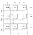
도 2는 본 개시의 실시예에 따른 화소 어레이(110)를 나타내는 블럭도이다. 화소 어레이(110)는 PXG1부터 PXGn으로 구성되는 n개의 화소 그룹(PXG1-PXGn)을 포함한다. 각각의 화소 그룹(PXG1-PXGn)은 복수개의 화소부(111)를 포함한다.2 is a block diagram illustrating a
예를 들어, 화소부(111)는 N×M 매트릭스 형태로 배치되며, 수평 라인에 배치된 복수의 화소부(111)들의 그룹을 화소 그룹(PXG1-PXGn) 중 하나로 설정할 수 있다. 반드시 동일 수평 라인의 화소부(111)들로만 화소 그룹(PXG1-PXGn)을 설정할 필요는 없으며, 예를 들어, 동일 수평 라인에 연결되지 않아도, 축적 동작을 동시에 수행하는 화소부(111)들로 화소 그룹(PXG1-PXGn)을 설정할 수 있다.For example, the
화소 그룹(PXG1-PXGn)에 포함되는 복수의 화소부(111)들은 리셋 신호(RG1-RGn), 전송 신호(TG1-TGn) 및 선택 신호(SEL1-SELn)를 수신한다.The plurality of
예를 들어, 첫 번째 화소 그룹(PXG1)에 포함되는 화소부(111)들은 제 1 리셋 신호(RG1), 제 1 전송 신호(TG1) 및 제 1 선택 신호(SEL1)를 수신한다. 마지막 번째 화소 그룹(PXGn)에 포함되는 화소부(111)들은 제 N 리셋 신호(RGn), 제 N 전송 신호(TGn), 제 N 선택 신호(SELn)를 수신한다.For example, the
화소 어레이(110)는 반드시 하나의 그룹 단위 별로 동작을 수행할 필요는 없으며, 두 개 또는 그 이상의 그룹 단위 별로 동작을 수행할 수 있다.The
또한, 복수의 화소 그룹(PXG1-PXGn)을 축적 기간(EIT1-EITn)이 서로 상이한 두 개의 그룹으로 구분하여 동작하는 화소 어레이(120)에도 본 개시의 실시예가 적용 가능하다.The embodiment of the present disclosure is also applicable to the
일 예로서, 화소 어레이(110)는 롤링 셔터(rolling shutter) 방식에 기초하여 동작을 수행할 수 있다. 화소 어레이(110)는 테트라 셀(TETRA CELL) 또는 역광보정(Wide Dynamic Range, WDR)방식에 기초하여 동작을 수행할 수도 있다As an example, the
화소 어레이(110)는 축적 기간(EIT1-EITn) 동안에 피사체로부터 반사되는 광에 대응하는 전하를 축적하는 축적 동작을 수행한다. 축적 동작은 복수개의 화소 그룹(PXG1-PXGn) 단위 별로 순차적으로 수행된다. The
화소 어레이(110)는 전송 기간(TP1-TPn) 동안에 축적된 전하를 화소 노드(FD)로 전송하는 전송 동작을 수행한다. 전송 동작은 복수개의 화소 그룹(PXG1-PXGn) 단위 별로 순차적으로 수행된다.The
화소 어레이(110)는 리드 아웃 기간(ROP1-ROPn) 동안에 화소 노드의 전위에 대응하는 신호를 생성하는 리드 아웃 동작을 수행한다. 리드 아웃 동작 역시 복수개의 화소 그룹(PXG1-PXGn) 단위 별로 순차적으로 수행된다. The
복수개의 화소 그룹(PXG1-PXGn)은 축적 동작을 순차적으로 수행하기 때문에, 각 화소 그룹(PXG1-PXGn) 별로 축적 기간(EIT1-EITn)의 기점과 종점이 서로 상이하다. 각각의 화소 그룹(PXG1-PXGn)에 있어서, 기점과 종점이 서로 상이한 축적기간 동안에 광 노출 시간(ET1-ETn)이 서로 동일하게 하기 위해, 제어부(120)는 광 제어 신호(ISYNC)를 생성한다.Since the plurality of pixel groups PXG1 to PXGn sequentially perform the accumulation operation, the starting point and the ending point of the accumulation periods EIT1 to EITn are different from each other for each of the pixel groups PXG1 to PXGn. The
각 화소 그룹(PXG1-PXGn) 별로 광 노출 시간(ET1-ETn)을 동일하게 하기 위해, 광 제어 신호(ISYNC)는 첫 번째 화소 그룹(PXG1)의 축적 기간(EIT1)동안에 적어도 1회 생성되고, 마지막 번째 화소 그룹(PXGn)의 축적 기간(EITn) 동안에 적어도 1회 생성 된다.The light control signal ISYNC is generated at least once during the accumulation period EIT1 of the first pixel group PXG1 to equalize the light exposure times ET1 to ETn for each pixel group PXG1 to PXGn, Is generated at least once during the accumulation period EITn of the last pixel group PXGn.
첫 번째 화소 그룹(PXG1)은 복수개의 화소 그룹(PXG1-PXGn) 중 축적 동작을 첫 번째로 수행하는 화소 그룹(PXG1-PXGn)중 하나이며, 마지막 번째 화소 그룹(PXGn)은 축적 동작을 마지막으로 수행하는 화소 그룹(PXG1-PXGn) 중 또 다른 하나이다. The first pixel group PXG1 is one of the pixel groups PXG1 to PXGn that performs the accumulation operation among the plurality of pixel groups PXG1 to PXGn first and the last pixel group PXGn is one of the pixel groups PXG1 to PXGn, Is another one of the pixel groups PXG1 to PXGn to be performed.
본 개시의 기술적 사상의 일 실시예에 따른 이미지 센서(100)는 동일한 광 노출 시간(ET1-ETn)에 기초하여 이미지를 생성하므로, 화소 그룹 단위 별 광 노출 시간(ET1-ETn)이 상이함에 따라 발생하는 이미지의 왜곡을 최소화하여 보다 더 선명한 이미지를 생성할 수 있다.Since the
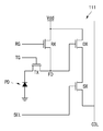
도 3은 본 개시의 실시예에 따른 화소부(111)를 나타내는 회로도로서, 화소부(111)는 리셋 트랜지스터(RX), 광 다이오드(PD), 전송 트랜지스터(TX), 구동 트랜지스터(DX), 및 출력 트랜지스터(SX)을 포함한다. 이에 대한 구체적인 설명은 화소부(111)가 개시된 한국 공개특허공보 제2012-0031403호를 참조한다. 3 is a circuit diagram showing a
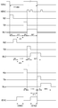
도 4 및 5 는 축적 기간(EIT1-EITn)이 리드 아웃 기간(ROP1-ROPn)이상인 경우에 각 화소 그룹(PXG1-PXGn)의 축적 기간(EIT1-EITn)과 광 제어 신호(ISYNC)의 타이밍을 나타내는 도면이다. 4 and 5 show the timing of the accumulation periods EIT1-EITn and light control signals ISYNC of the respective pixel groups PXG1-PXGn when the accumulation periods EIT1-EITn are equal to or greater than the readout periods ROP1-ROPn Fig.
도 4 에서는 축적 기간(EIT1-EITn)이 리드 아웃 기간(ROP1-ROPn)과 동일한 경우를 도시하였지만, 축적 기간(EIT1-EITn)이 리드 아웃 기간(ROP1-ROPn)을 초과하는 경우에도 동일하게 적용 가능하다.4 shows the case where the accumulation periods EIT1 to EITn are equal to the lead-out periods ROP1 to ROPn, but the same applies also when the accumulation periods EIT1 to EITn exceed the lead-out periods ROP1 to ROPn It is possible.
도 4 에 도시된 것과 같이, 제어부(120)는 마지막 번째 화소 그룹(PXGn)을 위한 리셋 신호(RGn)에 연동하여 발생되는 제 1 펄스(ISYNC1)와 마지막 번째 화소 그룹(PXGn)을 위한 전송 신호(TGn)에 연동하여 발생되는 제 2 펄스(ISYNC2)를 포함하는 광 제어 신호(ISYNC)를 생성할 수 있다4, the
도 4 에 도시된 광 제어 신호(ISYNC)의 활성화 시간 즉, 제 1 및 2 펄스(ISYNC1, ISYNC2)의 활성화 시간은 광이 발생하여 지속되는 시간을 의미한다. The activation time of the light control signal ISYNC shown in FIG. 4, that is, the activation time of the first and second pulses ISYNC1 and ISYNC2, means a time when light is generated and sustained.
제 1 펄스(ISYNC1)는 마지막 번째 화소 그룹(PXGn)에 대한 리셋 신호(RGn)가 발생되는 시점에 광이 발생되지 않도록 비활성화 상태가 될 수 있다. 또한, 제 2펄스(ISYNC2)는 마지막 번째 화소 그룹(PXGn)에 대한 전송 신호(TGn)가 발생되는 시점에 광이 발생되지 않도록 비활성화 상태가 될 수 있다. The first pulse ISYNC1 may be inactivated so that no light is generated at the time when the reset signal RGn for the last pixel group PXGn is generated. Also, the second pulse ISYNC2 may be inactivated so that no light is generated at the time when the transmission signal TGn for the last pixel group PXGn is generated.
다시 말해, 제 1펄스(ISYNC1)의 하강 에지(falling edge)는 마지막 번째 화소 그룹(PXGn)의 리셋 신호(RGn)가 발생하는 시점과 일치(align)할 수 있다. 제 2펄스(ISYNC2)의 하강 에지는 마지막 번째 화소 그룹(PXGn)의 전송 신호(TGn)가 발생하는 시점과 일치할 수 있다. In other words, a falling edge of the first pulse ISYNC1 may align with a time point at which the reset signal RGn of the last pixel group PXGn is generated. The falling edge of the second pulse ISYNC2 may coincide with the time point at which the transmission signal TGn of the last pixel group PXGn is generated.
축적 기간(EIT1-EITn)이 리드 아웃 기간(ROP1-ROPn)과 동일한 경우, 첫 번째 화소 그룹(PXG1)의 축적 기간(EIT1) 이후에 마지막 번째 화소 그룹(PXGn)의 축적기간(EITn)이 시작된다. 마지막 번째 화소 그룹(PXGn)의 축적 기간(EITn) 이전에 제 1펄스(ISYNC1)를 활성화하면, 마지막 번째 화소 그룹(PXGn)의 화소부(111)는 제 1펄스(ISYNC1)에 의해 발생된 광에 노출되지 못한다. 각 화소 그룹(PXG1-PXGn)의 광 노출 시간(ET1-ETn)을 서로 동일하게 하기 위하여, 제어부(120)는 마지막 번째 화소 그룹(PXGn)의 축적 기간(EITn)에 맞추어 제 2 펄스(ISYNC2)를 활성화 한다.The accumulation period EITn of the last pixel group PXGn starts after the accumulation period EIT1 of the first pixel group PXG1 when the accumulation periods EIT1 to EITn are equal to the readout periods ROP1 to ROPn do. When the first pulse ISYNC1 is activated before the accumulation period EITn of the last pixel group PXGn, the
도 4에 도시된 바와 같이, 첫 번째 화소 그룹(PXG1)의 광 노출 시간(ET1), 두 번째 화소 그룹(PXG2)의 광 노출 시간(ET2) 그리고 마지막 번째 화소 그룹(PXGn)의 광 노출 시간(ETn)이 서로 동일한 것을 알 수 있다.The light exposure time ET1 of the first pixel group PXG1, the light exposure time ET2 of the second pixel group PXG2 and the light exposure time of the last pixel group PXGn ETn are equal to each other.
또한, 도 4에 도시된 것과 같이 제어부(120)는 수직 동기 신호(VSYNC)에 연동하여 광 제어 신호(ISYNC)를 생성할 수 있다. In addition, as shown in FIG. 4, the
수직 동기 신호(VSYNC)는 하나의 이미지 프레임을 구분하는 신호이다. 예를 들어, 수직 동기 신호(VSYNC)가 한 번 활성화되었다면, 이는 하나의 이미지 프레임이 생성되었음을 의미한다.The vertical synchronization signal VSYNC is a signal for distinguishing one image frame. For example, if the vertical sync signal VSYNC has been activated once, this means that one image frame has been generated.
이 때의 광 제어 신호(ISYNC)는 제 1 펄스(ISYNC1)와 제 2 펄스(ISYNC2)를 포함할 수 있다. 제 1 펄스(ISYNC1)는 수직 동기 신호(VSYNC)의 활성화 시점에 광이 발생되지 않도록, 비활성화된다. 제 2 펄스(ISYNC2)는 수직 동기 신호(VSYNC)의 비활성화 시점에 광이 발생되지 않도록, 비활성화된다.The light control signal ISYNC at this time may include a first pulse ISYNC1 and a second pulse ISYNC2. The first pulse ISYNC1 is inactivated so that no light is generated at the time of activation of the vertical synchronization signal VSYNC. The second pulse ISYNC2 is inactivated so that no light is generated at the time of deactivation of the vertical synchronization signal VSYNC.
또한, 제어부(120)는 수평 동기 신호(HSYNC)에 연동하여 광 제어 신호(ISYNC)를 생성할 수 있다. 수평 동기 신호(HSYNC)는 화소 그룹(PXG1-PXGn) 에서 생성되는 화소 신호의 전송을 동기화하는 신호이다. In addition, the
또 다른 예를 들어, 제 1펄스(ISYNC1)는 첫 번째 화소 그룹(PXG1)의 전송 신호(TG1)에 연동할 수 있으며 제 2펄스(ISYNC2)는 첫 번째 화소 그룹(PXG1)의 선택 신호(SEL1)에 연동할 수 있다. For example, the first pulse ISYNC1 may be coupled to the transmission signal TG1 of the first pixel group PXG1 and the second pulse ISYNC2 may be coupled to the selection signal SEL1 of the first pixel group PXG1. ).
그 밖에 제어부(120)는 이미지 프레임의 생성을 시작하는 셔터 신호, 리셋 신호(RG1-RGn), 전송 신호(TG1-TGn) 및 선택 신호(SEL1-SELn) 또는 기타 신호와 연동하여 광 제어신호를 생성할 수 있다. 또는, 제어부(120)는 사용자에 의해 미리 설정된 프로그램에 따라 광 제어신호를 생성할 수도 있다.In addition, the
각 화소 그룹(PXG1-PXGn)이 동일한 광 노출 시간(ET1-ETn)을 가질 수 있다면 다양한 신호의 조합에 따라 광 제어 신호(ISYNC)를 활성화 할 수 있다.It is possible to activate the light control signal ISYNC according to various signal combinations if each pixel group PXG1-PXGn can have the same light exposure time ET1-ETn.
본 개시의 실시예는 광 발생의 지속 시간을 조정할 수 있다. 예를 들어, 제어부(120)는 제 1 및 2펄스(ISYNC1, ISYNC2)의 폭을 조정하여 광 발생 지속시간을 조정할 수 있다. 제어부(120)는 도 4에 도시된 제 1 및 2펄스(ISYNC1, ISYNC2)의 폭을 도5 에 도시된 제 1 및 2펄스(ISYNC1, ISYNC2)의 폭과 같이 넓힐 수 있다. Embodiments of the present disclosure can adjust the duration of light generation. For example, the
제어부(120)는 다양한 환경 속에서 피사체의 인식률을 높이기 위해 광 제어 신호(ISYNC)의 활성화 시간을 조정할 수 있다. 다만, 축적 기간(EIT1-EITn)의 전 구간에 걸쳐 광이 발생되는 것을 방지하기 위해, 제어부(120)는 제 1 펄스(ISYNC1)와 제 2펄스(ISYNC2)를 비연속적으로 활성화할 수 있다. The
이로 인하여 본 개시의 실시예는 광의 지속 시간을 조절함으로써 다양한 환경에 맞추어 신호대잡음비(SNR)을 개선하거나 광 발생으로 인한 전력 소모를 조절할 수 있다.Thus, embodiments of the present disclosure can improve the signal-to-noise ratio (SNR) according to various environments by adjusting the duration of the light or adjust the power consumption due to light generation.
도 6 은 축적 기간(EIT1-EITn)이 리드 아웃 기간(ROP1-ROPn)보다 짧으며, 리드 아웃 기간(ROP1-ROPn)과 광 제어 신호(ISYNC)의 활성화 시간을 더한 시간의 절반 이상인 경우, 각 화소 그룹(PXG1-PXGn) 의 축적 기간(EIT1-EITn)과 광 제어 신호(ISYNC)의 타이밍을 나타내는 도면이다. 여기서, 광 제어 신호(ISYNC)의 활성화 시간은 각각의 제 1 및 2펄스(ISYNC1, ISYNC2)의 폭을 의미할 수 있다6 shows a case where the accumulation periods EIT1 to EITn are shorter than the lead-out periods ROP1 to ROPn and are equal to or more than half of the times obtained by adding the activation periods of the lead-out periods ROP1 to ROPn and the light control signal ISYNC, (EIT1-EITn) of the pixel groups PXG1-PXGn and the timing of the light control signal ISYNC. Here, the activation time of the light control signal ISYNC may mean the width of each of the first and second pulses ISYNC1 and ISYNC2
다시 말해 축적 기간(EIT1-EITn)이 아래의 식 1을 만족하는 경우에. 제어부(120)는 첫 번째 화소 그룹(PXG1)을 위한 전송 신호(TG1)에 연동하여 발생되는 제 1펄스(ISYNC1)와 마지막 번째 화소 그룹(PXGn)을 위한 전송 신호(TGn)에 연동하여 발생되는 제 2펄스(ISYNC2)를 포함하는 광 제어 신호(ISYNC)를 생성할 수 있다.In other words, when the accumulation period (EIT1-EITn) satisfies the following expression (1). The
[식 1][Formula 1]
ROP > EIT ≥ (ROP + PULSE_WIDTH)/2ROP > EIT > (ROP + PULSE_WIDTH) / 2
(ROP=리드 아웃 기간(ROP1-ROPn), EIT=축적 기간(EIT1-EITn), PULSE_WIDTH=광 제어 신호(ISYNC)의 1회의 활성화 시간)(Activation times of ROP = lead-out period (ROP1-ROPn), EIT = accumulation period (EIT1-EITn), PULSE_WIDTH = light control signal (ISYNC)
이때, 제 1펄스(ISYNC1)는 첫 번째 화소 그룹(PXG1)에 대한 전송 신호(TG1)가 발생되는 시점에 광이 발생되지 않도록 비활성화 상태가 될 수 있다. 또한, 제 2펄스(ISYNC2)는 마지막 번째 화소 그룹(PXGn)에 대한 전송 신호(TGn)가 발생되는 시점으로부터 리드 아웃 기간(ROP1-ROPn)에서 축적 기간(EIT1-EITn)을 뺀 시간(ROP-EIT)만큼 앞서서 광이 발생되지 않도록 비활성화 상태가 될 수 있다.At this time, the first pulse ISYNC1 may be inactivated so that no light is generated at the time when the transmission signal TG1 for the first pixel group PXG1 is generated. The second pulse ISYNC2 is a time interval obtained by subtracting the accumulation period EIT1-EITn from the lead-out period ROP1-ROPn from the time when the transmission signal TGn for the last pixel group PXGn is generated, EIT) in order to prevent light from being generated.
다시 말해, 제 1펄스(ISYNC1)의 하강 에지는 첫 번째 화소 그룹(PXG1)의 전송 신호(TG1)가 발생하는 시점과 일치할 수 있다. 제 2펄스(ISYNC2)의 하강 에지는 마지막 번째 화소 그룹(PXGn)의 전송 신호(TGn)가 발생하는 시점에서 (ROP-EIT) 만큼 앞서는 시점에 일치할 수 있다. In other words, the falling edge of the first pulse ISYNC1 may coincide with the time point at which the transmission signal TG1 of the first pixel group PXG1 is generated. The falling edge of the second pulse ISYNC2 may coincide with a time point ahead of the transmission signal TGn of the last pixel group PXGn by (ROP-EIT).
도 6 에 도시된 바와 같이, 첫 번째 화소 그룹(PXG1)의 광 노출 시간(ET1), N-1 번째 화소 그룹(PXGn-1)의 광 노출 시간(ETn-1) 그리고 마지막 번째 화소 그룹(PXGn)의 광 노출 시간(ETn)이 서로 동일한 것을 알 수 있다6, the light exposure time ET1 of the first pixel group PXG1, the light exposure time ETn-1 of the (N-1) th pixel group PXGn-1, and the light exposure time ETn- ) Are equal to each other
도 6 과 같이 리드 아웃 기간(ROP1-ROPn)이 축적 기간(EIT1-EITn)이상인 경우, 이미지 센서(100)에서 고속의 신호 처리가 필요한 것이 아니기 때문에 신호 처리 회로의 설계 복잡도와 면적의 증가를 방지할 수 있고, 신호처리를 위한 전력 소모의 증가도 방지할 수 있다. 6, when the lead-out periods ROP1 to ROPn are equal to or more than the accumulation periods EIT1 to EITn, since the
도 7 및 8 은 본 개시의 기술적 사상의 일실시예에 따른 제어부(120)를 도시한 블록도이다.Figures 7 and 8 are block diagrams illustrating a
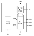
도 7 에 도시된 바와 같이 제어부(120)는 타이밍 발생부(121)와 로우 제어부(122)를 포함할 수 있다. As shown in FIG. 7, the
타이밍 발생부(121)는 수직 동기 신호(VSYNC) 및 수평 동기 신호(HSYNC)를 생성하여 로우 제어부(122)나 외부로 송신할 수 있다. 또한, 타이밍 발생부(121) 내부에서 이미지 센서(100)에서 처리되는 신호를 위한 클락(clock) 펄스를 생성할 수 있다. 또는 별도의 클락 생성기(미도시)에서 클락 펄스가 생성되고, 타이밍 발생부(121)가 클락 펄스를 수신할 수 있다. 타이밍 발생부(121)는 클락에 기초하여 수직 동기 신호(VSYNC), 수평 동기 신호(HSYNC)를 비롯한 이미지 센서(100)에서 처리되는 신호의 타이밍을 제어한다.The
로우 제어부(122)는 수직 동기 신호(VSYNC) 및 수평 동기 신호(HSYNC)에 기초하여, 복수개의 화소 그룹(PXG1-PXGn) 들에 대응하여 복수개의 리셋 신호(RG1-RGn), 전송 신호(TG1-TGn), 선택 신호(SEL1-SELn)들을 순차적으로 발생한다.The
로우 제어부(122)는 복수의 화소 그룹(PXG1-PXGn) 의 축적 기간(EIT1-EITn) 동안에 광에 노출되는 시간이 각 화소 그룹(PXG1-PXGn) 별로 서로 동일하도록 광 제어 신호(ISYNC)를 생성할 수 있다.The
도 8에 도시된 것과 같이, 제어부(120)는 타이밍 발생부(121), 로우 제어부(122) 및 광 제어 신호 발생부(123)를 포함할 수 있다.8, the
타이밍 발생부(121)는 수직 동기 신호(VSYNC) 및 수평 동기 신호(HSYNC)등을 생성하며, 로우 제어부(122)는 리셋 신호(RG1-RGn), 전송 신호(TG1-TGn) 및 선택 신호(SEL1-SELn)를 화소 그룹(PXG1-PXGn) 별로 순차적으로 생성한다.The
광 제어 신호 발생부(123)는 복수의 화소 그룹(PXG1-PXGn)의 축적 기간(EIT1-EITn) 동안에 광에 노출되는 시간이 각 화소 그룹(PXG1-PXGn)별로 서로 동일하도록 광 제어 신호(ISYNC)를 생성할 수 있다. 예를 들어, 광 제어 신호 발생부(123)는 펄스 발생기일 수 있다.The light control
광 제어 신호 발생부(123)는 로우 제어부(122)로부터 수신한 신호(Sx,Sy)에 기초하여 광 제어 신호(ISYNC)를 생성한다. 신호(Sx,Sy)는 화소 그룹(PXG1-PXGn)의 축적 기간(EIT1-EITn) 중에 광 노출 시간(ET1-ETn)이 서로 동일하기 위한 다양한 조합의 신호일 수 있다.The light control
광 제어 신호(ISYNC)는 축적 동작 및 리드 아웃 동작을 제어하는 제어부(120)에서 생성되기 때문에, 본 개시의 기술적 사상의 일 실시예는 화소 그룹(PXG1-PXGn)의 축적 동작 타이밍에 정확하게 맞추어 광 제어 신호(ISYNC)를 활성화 할 수 있다. Since the light control signal ISYNC is generated by the
이하, 도 9 및 10을 참조하여 본 개시의 기술적 사상의 일 실시예에 따른 전자 장치를 설명하도록 한다. 이와 관련하여 상술한 본 개시의 구성과 중복되는 것은 생략하거나 간략히 기술하도록 한다.Hereinafter, an electronic device according to an embodiment of the technical idea of the present disclosure will be described with reference to FIGS. 9 and 10. FIG. In this regard, the elements overlapping with those of the present disclosure described above will be omitted or briefly described.
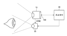
도 9에 도시된 바와 같이, 전자 장치는 앞서 설명한 이미지 센서를 구비하는 카메라(10), 발광 모듈(20) 및 프로세서(30)를 포함한다. As shown in Fig. 9, the electronic device includes a
발광 모듈(20)은 이미지 센서(100) 또는 프로세서(30)에서 발생한 광 제어 신호(ISYNC)에 연동하여 광을 피사체에 조사한다. 예를 들어 피사체는 인간의 홍채일 수 있다. 발광 모듈(20)은 적외선 광을 발생하는 적외선 LED를 포함할 수 있다.The
발광 모듈(20)은 광이 발생하여 지속되는 시간을 결정할 수 있다. 예를 들어, 광 제어 신호(SIYNC)가 활성화되면 광을 생성하고, 발광 모듈(20)의 제어에 따라 소정의 시간 동안 광의 발생을 지속할 수 있다. 또는 프로세서(30)의 제어에 의해 광의 지속 시간을 결정할 수도 있다.The
프로세서(30)는 미리 설정된 어플리케이션 프로그램을 실행하여 발생하는 제어신호를 통해 카메라(10)의 구동을 제어할 수 있다. 프로세서(30)는 어플리케이션 프로그램에 따라 이미지 센서(100)가 광 제어 신호(ISYNC)를 생성하도록 카메라(10)의 이미지 센서(100)를 제어할 수 있다. 예를 들어, 어플리케이션 프로그램이 구동되고 사용자에 의해 촬영 명령이 입력되는 경우, 프로세서(30)는 이미지 센서(100)가 광 제어 신호(ISYNC)를 생성하라는 제어 신호를 이미지 센서(100)로 전송할 수 있다.The
또한, 프로세서(30)는 이미지 프레임을 생성하는 동안, 광이 적어도 2번 이상 발생될 수 있도록, 광의 발생을 제어하는 광 제어 신호(ISYNC)를 직접 생성할 수 있다. In addition, the
프로세서(30)는 어플리케이션 프로그램에 따라 사용자의 홍채 이미지 프레임을 분석한다. 예를 들어, 프로세서(30)는 인증 어플리케이션 프로그램에 따라 홍채 이미지 프레임을 분석하여 사용자를 인증할 수 있다. 프로세서(30)는 홍채 이미지를 미리 등록된 홍채 특징 패턴과 비교하여, 일치하는 패턴이 일정 이상인 경우, 인증이 성공한 것으로 간주할 수 있다. 다만 이는 예시적인 것으로, 홍채 이미지를 이용하여 사용자를 인증할 수 있는 것이라면 본 개시의 기술적 사상에 적용 가능하다.The
프로세서(30)는 예를 들어, 중앙처리장치(CPU: central processing unit), 어플리케이션 프로세서(AP: application processor) 또는 커뮤니케이션 프로세서(CP: communication processor) 중 어느 하나일 수 있다.The
카메라(10)는 발광 모듈(20)에서 발생하는 광을 이용하여 이미지를 획득하며, 이미지를 프로세서(30)로 송신할 수 있다. 카메라(10)은 렌즈 및 이미지 센서(100)를 포함한다. 렌즈는 피사체에 의해 반사되는 광을 받아들인다.The
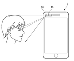
도 10는 본 개시의 기술적 사상의 일실시예에 따른 전자 장치가 스마트 폰(1)에 적용된 것을 도시한 도면이다. 발광 모듈(20)은 적외선 LED를 포함할 수 있으며 사용자의 눈 주위영역에 적외선 광을 조사할 수 있다. 사용자로부터 반사되는 적외선 광이 카메라 모듈(10)의 렌즈를 통해 입사하고, 적외선 광에 의해 홍채 이미지를 획득한다.10 is a diagram showing that an electronic device according to an embodiment of the technical idea of the present disclosure is applied to the
다만, 스마트 폰(1)은 예시적인 것으로, 전자 장치가 적용될 수 있는 것으로는 태블릿 PC(tablet personal computer), 이동전화기(mobile phone), 화상전화기, 전자북 리더기(e-book reader), 데스크탑 PC(desktop personal computer), 랩탑 PC(laptop personal computer), 넷북 컴퓨터(netbook computer), PDA(personal digital assistant),PMP(portable multimedia player), MP3 플레이어, 모바일 의료기기, 카메라(camera), 또는 웨어러블 장치(wearable device)(예: 전자 안경과 같은 head-mounted-device(HMD), 전자 의복, 전자 팔찌, 전자 목걸이, 전자 앱세서리(appcessory), 또는 스마트 와치(smartwatch)중 적어도 하나를 포함할 수 있다. However, the
이하, 도 11 및 도12를 참조하여 본 개시의 기술적 사상의 일 실시예에 따른 이미지 센서의 광 제어신호 발생 방법을 설명하도록 한다. 이와 관련하여 상술한 본 개시의 구성과 중복되는 것은 생략하거나 간략히 기술하도록 한다.Hereinafter, a method of generating the light control signal of the image sensor according to an embodiment of the technical idea of the present disclosure will be described with reference to FIGS. 11 and 12. FIG. In this regard, the elements overlapping with those of the present disclosure described above will be omitted or briefly described.
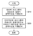
첫 번째 화소 그룹(PXG1)의 복수개의 화소부(111)들이 입사되는 광에 대응하는 전하를 축적하는 축적 기간(EIT1) 동안에, 광을 발생하기 위한 광 제어 신호(ISYNC)를 적어도 1회 활성화 한다.The light control signal ISYNC for generating light is activated at least once during the accumulation period EIT1 in which the plurality of
다음으로, 마지막 번째 화소 그룹(PXGn)의 복수개의 화소부(111)들이 광에 대응하는 전하를 축적하는 축적 기간(EITn) 동안에 광 제어 신호(ISYNC)를 적어도 1회 활성화한다Next, the plurality of
구체적으로, 축적 기간(EIT1-EITn)이 리드 아웃 기간(ROP1-ROPn) 이상인 경우, 제어부(120)는 마지막 번째 화소 그룹(PXGn)에 대한 리셋 신호(RGn)가 발생되는 시점에 광이 발생하지 않도록 광 제어 신호(ISYNC)를 비활성화한다.(S110) 또한, 마지막 번째 화소 그룹(PXGn)에 대한 전송 신호(TGn)가 발생되는 시점에 광이 발생하지 않도록 광 제어 신호(ISYNC)를 비활성화한다.(S120) Specifically, when the accumulation periods EIT1-EITn are equal to or greater than the readout periods ROP1-ROPn, the
축적 기간(EIT1-EITn)이 상술한 식1을 만족하는 경우 제어부(120)는 첫 번째 화소 그룹(PXG1)에 대한 전송 신호(TG61)가 발생되는 시점에 광이 발생하지 않도록 광 제어 신호(ISYNC)를 비활성화한다.(S210) 또한, 마지막 번째 화소 그룹(PXGn)에 대한 전송 신호(TGn)가 발생되는 시점으로부터 리드 아웃 기간(ROP1-ROPn)에서 축적 기간(EIT1-EITn)을 뺀 시간(ROP-EIT)만큼 앞서서 광이 발생하지 않도록 광 제어 신호(ISYNC)를 비활성화한다.(S220)When the accumulation periods EIT1-EITn satisfy the above-described
S210,S220 단계와 같이, 리드 아웃 기간(ROP1-ROPn)은 축적 기간(EIT1-EITn)보다 더 길게 설정할 수 있다. 리드 아웃 기간(ROP1-ROPn)이 길어짐에 따라 이미지 센서(100)에서 고속의 신호 처리가 필요한 것이 아니기 때문에 신호 처리 회로의 설계 복잡도와 면적의 증가를 방지할 수 있고, 신호처리를 위한 전력 소모의 증가도 방지할 수 있다. The readout periods ROP1 to ROPn may be set longer than the accumulation periods EIT1 to EITn as in the steps S210 and S220. Since the
본 개시에 따른 상기 다양한 실시예에 따라 화소 그룹(PXG1-PXGn) 별로 광 노출 시간(ET1-ETn)을 동일하게 하고, 광 제어 신호(ISYNC)의 활성화 시간을 효율적으로 제어함으로써 화질을 개선하면서 전력 소모를 줄이는 이미지 센서(100)를 제공할 수 있다.The light exposure time ET1-ETn is equalized for each of the pixel groups PXG1-PXGn according to the various embodiments according to the present disclosure and the activation time of the light control signal ISYNC is effectively controlled, It is possible to provide an
이상, 첨부된 도면을 참조하여 본 개시에 따른 실시 예들을 설명하였지만, 본 발명이 속하는 기술 분야에서 통상의 지식을 가진 자는 본 발명이 그 기술적 사상이나 필수적인 특징을 변경하지 않고서 다른 구체적인 형태로 실시될 수 있다는 것을 이해할 수 있을 것이다. 이상에서 기술한 실시 예는 모든 면에서 예시적인 것이며 한정적이 아닌 것으로 이해하여야 한다.While the present invention has been described in connection with what is presently considered to be practical exemplary embodiments, it is to be understood that the invention is not limited to the disclosed embodiments, but, on the contrary, You can understand that you can. It should be understood that the above-described embodiments are illustrative and non-restrictive in every respect.
1 : 스마트 폰
10 : 카메라 모듈
20 : 적외선 발광 모둘
30 : 프로세서
100 : 이미지 센서
110 : 화소 어레이
111 : 화소부
120 : 제어부
121 : 타이밍 발생부
122 : 로우 제어부
123 : 광 제어 신호 발생부
130 : 아날로그-디지털 변환기
140 : 데이터 출력부
ISYNC : 광 제어 신호
VSYNC : 수직 동기 신호
HYSYNC : 수평 동기 신호
EIT1-EITn : 축적 기간
TP1-TPn : 전송 기간
ET1-ETn : 광 노출 시간
ROP1-ROPn : 리드 아웃 기간
RP1-RPn : 리셋 기간
PXG1-PXGn : 화소 그룹
RG1-RGn : 리셋 신호
TG1-TGn : 전송 신호
SEL1-SELn : 선택 신호
PD : 광 다이오드
RX : 리셋 트랜지스터
TX : 전송 트랜지스터
DX : 드라이버 트랜지시터
SX : 선택 트랜지스터1: Smartphone 10: Camera module
20: Infrared ray emitting module 30: Processor
100: image sensor 110: pixel array
111: pixel unit 120:
121: Timing generator 122:
123: light control signal generator 130: analog-to-digital converter
140: Data output unit ISYNC: Light control signal
VSYNC: Vertical sync signal HYSYNC: Horizontal sync signal
EIT1-EITn: accumulation period TP1-TPn: transfer period
ET1-ETn: light exposure time ROP1-ROPn: lead-out period
RP1-RPn: reset period PXG1-PXGn: pixel group
RG1-RGn: reset signal TG1-TGn:
SEL1-SELn: selection signal PD: photodiode
RX: reset transistor TX: transfer transistor
DX: driver transistor indicator SX: selection transistor
Claims (10)
이미지 프레임을 생성하는 동안, 상기 화소부들이 피사체로부터 반사되는 광에 적어도 2번 이상 노출될 수 있도록, 상기 광을 제어하는 광 제어신호를 생성하는 제어부를 포함하는 이미지 센서.A pixel array including a plurality of pixel portions; And
And a control unit for generating a light control signal for controlling the light so that the pixel units can be exposed to light reflected from the subject at least twice during generation of the image frame.
상기 화소 어레이는
복수개의 화소 그룹들로 나뉘어진 복수개의 화소부들을 구비하고,
리셋 신호에 연동하여 화소 노드의 전위를 초기화하는 리셋 동작과, 축적 기간 동안 상기 광에 대응하는 전하를 축적하는 축적 동작과, 전송 신호에 연동하여 상기 축적된 전하를 상기 화소 노드로 전송하는 전송 동작과, 리드 아웃 기간 동안 상기 축적된 전하에 대응하는 화소 노드의 전위의 변화에 기초하여 화소 신호를 생성하는 리드 아웃 동작과, 선택 신호에 연동하여 상기 화소 신호를 출력하는 출력동작을, 상기 화소 그룹 단위 별로 순차적으로 수행하는 이미지 센서.The method according to claim 1,
The pixel array
And a plurality of pixel units divided into a plurality of pixel groups,
A reset operation for resetting the potential of the pixel node in response to a reset signal, a accumulation operation for accumulating the charge corresponding to the light during the accumulation period, a transfer operation for transferring the accumulated charge to the pixel node, Out operation for generating a pixel signal based on a change in the potential of the pixel node corresponding to the accumulated charge during the readout period and an output operation for outputting the pixel signal in conjunction with the selection signal, An image sensor that performs sequential processing by unit.
상기 제어부는
상기 복수개의 화소 그룹들 중 첫 번째 화소 그룹의 상기 축적 기간 동안에 적어도 1회, 마지막 번째 화소 그룹의 상기 축적 기간 동안에 적어도 1회 상기 광이 발생하도록 상기 광 제어 신호를 생성하는 이미지 센서.3. The method of claim 2,
The control unit
Wherein the light control signal is generated so that the light is generated at least once during the accumulation period of at least one of the plurality of pixel groups and during the accumulation period of the first pixel group.
상기 제어부는
상기 축적 기간이 상기 리드 아웃 기간 이상인 경우,
상기 마지막 번째 화소 그룹을 위한 상기 리셋 신호에 연동하여 발생되는 제 1 펄스와 상기 마지막 번째 화소 그룹을 위한 상기 전송 신호에 연동하여 발생되는 제 2 펄스를 포함하는 상기 광 제어 신호를 생성하는 이미지 센서.The method of claim 3,
The control unit
When the accumulation period is equal to or longer than the lead-out period,
And generates a light control signal including a first pulse generated in conjunction with the reset signal for the last pixel group and a second pulse generated in conjunction with the transmission signal for the last pixel group.
상기 제 1 펄스는 상기 마지막 번째 화소 그룹을 위한 상기 리셋 신호가 발생되는 시점에 비활성화되고,
상기 제 2 펄스는 상기 마지막 번째 화소 그룹을 위한 상기 전송 신호가 발생되는 시점에 비활성화되는 이미지 센서5. The method of claim 4,
The first pulse is deactivated at the time when the reset signal for the last pixel group is generated,
Wherein the second pulse is an image signal which is inactivated at the time when the transmission signal for the last pixel group is generated,
상기 제어부는
상기 축적 기간이 상기 리드 아웃 기간보다 짧고, 상기 리드 아웃 기간과 상기 광 제어 신호의 활성화 시간을 더한 시간의 절반 이상인 경우,
상기 첫 번째 화소 그룹을 위한 상기 전송 신호에 연동하여 발생되는 제 1 펄스와 상기 마지막 번째 화소 그룹을 위한 상기 전송 신호에 연동하여 발생되는 제 2 펄스를 포함하는 상기 광 제어 신호를 생성하는 이미지 센서.The method of claim 3,
The control unit
When the accumulation period is shorter than the lead-out period and is equal to or longer than half of the time period in which the lead-out period and the activation period of the light control signal are added,
And generates a light control signal including a first pulse generated in conjunction with the transmission signal for the first pixel group and a second pulse generated in conjunction with the transmission signal for the last pixel group.
상기 제 1 펄스는 상기 첫 번째 화소 그룹을 위한 상기 전송 신호가 발생되는 시점에 비활성화되며,
상기 제 2 펄스는 상기 마지막 번째 화소 그룹을 위한 상기 전송 신호가 발생되는 시점으로부터 상기 리드 아웃 기간에서 상기 축적 기간을 뺀 시간만큼 앞선 시점에 비활성화되는 이미지 센서.The method according to claim 6,
Wherein the first pulse is deactivated at the time when the transmission signal for the first pixel group is generated,
Wherein the second pulse is inactivated at a time point earlier than a time obtained by subtracting the accumulation period from the lead-out period from a time point at which the transmission signal for the last pixel group is generated.
상기 제어부는
수직 동기 신호에 연동하여 상기 광 제어신호를 발생하는 이미지 센서The method of claim 3,
The control unit
An image sensor for generating the light control signal in synchronization with the vertical synchronization signal;
상기 제어부는
상기 수직 동기 신호의 활성화 시점에 상기 광이 발생되지 않도록, 비활성화 되는 제 1 펄스와 상기 수직 동기 신호의 비활성화 시점에 상기 광이 발생되지 않도록, 비활성화되는 제 2 펄스를 포함하는 상기 광 제어신호를 생성하는 이미지 센서.9. The method of claim 8,
The control unit
Generating a light control signal including a first pulse that is inactivated so that the light is not generated at the activation timing of the vertical synchronization signal and a second pulse that is inactivated so that the light is not generated at the time of deactivation of the vertical synchronization signal; Image sensor.
상기 제어신호에 응답하여 이미지 프레임을 생성하는 동안, 복수개의 화소부들이 피사체에 반사되는 광에 적어도 2번 이상 노출될 수 있도록, 상기 광을 제어하는 광 제어신호를 생성하는 이미지 센서를 구비하는 카메라;및
상기 광 제어 신호에 연동하여 상기 광이 생성되는 발광 모듈을 포함하는 전자 장치.
A processor for executing an application program to generate a control signal;
A camera having an image sensor for generating a light control signal for controlling the light so that a plurality of pixel units are exposed to light reflected by the subject at least twice during generation of an image frame in response to the control signal; ; And
And a light emitting module in which the light is generated in conjunction with the light control signal.
Priority Applications (3)
| Application Number | Priority Date | Filing Date | Title |
|---|---|---|---|
| KR1020170069566A KR20180133076A (en) | 2017-06-05 | 2017-06-05 | Image sensor and electronic apparatus including the same |
| US15/866,041 US10565447B2 (en) | 2017-06-05 | 2018-01-09 | Image sensor and electronic apparatus including the same |
| CN201810261907.1A CN108989714A (en) | 2017-06-05 | 2018-03-27 | Imaging sensor and electronic device including the imaging sensor |
Applications Claiming Priority (1)
| Application Number | Priority Date | Filing Date | Title |
|---|---|---|---|
| KR1020170069566A KR20180133076A (en) | 2017-06-05 | 2017-06-05 | Image sensor and electronic apparatus including the same |
Publications (1)
| Publication Number | Publication Date |
|---|---|
| KR20180133076A true KR20180133076A (en) | 2018-12-13 |
Family
ID=64458888
Family Applications (1)
| Application Number | Title | Priority Date | Filing Date |
|---|---|---|---|
| KR1020170069566A KR20180133076A (en) | 2017-06-05 | 2017-06-05 | Image sensor and electronic apparatus including the same |
Country Status (3)
| Country | Link |
|---|---|
| US (1) | US10565447B2 (en) |
| KR (1) | KR20180133076A (en) |
| CN (1) | CN108989714A (en) |
Families Citing this family (4)
| Publication number | Priority date | Publication date | Assignee | Title |
|---|---|---|---|---|
| US20190141264A1 (en) * | 2016-05-25 | 2019-05-09 | Mtekvision Co., Ltd. | Driver's eye position detecting device and method, imaging device having image sensor with rolling shutter driving system, and illumination control method thereof |
| KR20200086429A (en) * | 2019-01-09 | 2020-07-17 | 삼성전자주식회사 | Image signal processor, image processing system, and operating method of image signal processor |
| CN113330729A (en) * | 2019-01-25 | 2021-08-31 | 剑桥机电有限公司 | Improvements in and relating to PWM synchronisation |
| CN115379147B (en) * | 2022-09-14 | 2023-02-03 | 脉冲视觉(北京)科技有限公司 | Signal readout circuit, method and system, pixel unit array circuit and equipment |
Family Cites Families (16)
| Publication number | Priority date | Publication date | Assignee | Title |
|---|---|---|---|---|
| JP2002514098A (en) | 1996-08-25 | 2002-05-14 | センサー インコーポレイテッド | Device for iris acquisition image |
| FI111417B (en) * | 2001-06-01 | 2003-07-15 | Nokia Corp | Control of flash light in a digital camera |
| US7234641B2 (en) | 2004-12-01 | 2007-06-26 | Datalogic Scanning, Inc. | Illumination pulsing method for a data reader |
| US7430365B2 (en) | 2005-03-31 | 2008-09-30 | Avago Technologies Ecbu (Singapore) Pte Ltd. | Safe eye detection |
| TWI268398B (en) * | 2005-04-21 | 2006-12-11 | Sunplus Technology Co Ltd | Exposure controlling system and method thereof for image sensor provides a controller device driving the illuminating device to generate flashlight while each pixel row in subsection of an image is in exposure condition |
| US8953849B2 (en) | 2007-04-19 | 2015-02-10 | Eyelock, Inc. | Method and system for biometric recognition |
| KR101674099B1 (en) | 2010-10-14 | 2016-11-08 | 현대모비스 주식회사 | Apparatus for generating image for face authentication and method thereof |
| JP2013005017A (en) * | 2011-06-13 | 2013-01-07 | Sony Corp | Image pickup apparatus, image pickup apparatus control method, and program |
| US9332193B2 (en) * | 2011-11-14 | 2016-05-03 | Omnivision Technologies, Inc. | Synchronization of image acquisition in multiple image sensors with a synchronization clock signal |
| KR101323483B1 (en) | 2012-07-16 | 2013-10-31 | 아이리텍 잉크 | Dual mode camera for normal and iris image capturing |
| WO2015102704A2 (en) | 2013-10-08 | 2015-07-09 | Sri International | Iris biometric recognition module and access control assembly |
| KR20150075906A (en) * | 2013-12-26 | 2015-07-06 | 삼성전기주식회사 | Apparatus and mehtod for eye tracking |
| WO2015131198A1 (en) | 2014-02-28 | 2015-09-03 | Lrs Identity, Inc. | Dual iris and color camera in a mobile computing device |
| US10262203B2 (en) * | 2014-09-02 | 2019-04-16 | Samsung Electronics Co., Ltd. | Method for recognizing iris and electronic device therefor |
| US9961258B2 (en) | 2015-02-23 | 2018-05-01 | Facebook, Inc. | Illumination system synchronized with image sensor |
| US10009554B1 (en) * | 2017-02-24 | 2018-06-26 | Lighthouse Ai, Inc. | Method and system for using light emission by a depth-sensing camera to capture video images under low-light conditions |
-
2017
- 2017-06-05 KR KR1020170069566A patent/KR20180133076A/en unknown
-
2018
- 2018-01-09 US US15/866,041 patent/US10565447B2/en active Active
- 2018-03-27 CN CN201810261907.1A patent/CN108989714A/en active Pending
Also Published As
| Publication number | Publication date |
|---|---|
| CN108989714A (en) | 2018-12-11 |
| US10565447B2 (en) | 2020-02-18 |
| US20180349697A1 (en) | 2018-12-06 |
Similar Documents
| Publication | Publication Date | Title |
|---|---|---|
| KR20180133076A (en) | Image sensor and electronic apparatus including the same | |
| US11317044B2 (en) | Solid state imaging device and method of controlling solid state imaging device | |
| JP6029286B2 (en) | Photoelectric conversion device and imaging system | |
| KR102503442B1 (en) | Electronic device and operating method thereof | |
| KR20140005421A (en) | Image sensor chip, operation method thereof, and system having the same | |
| US9876978B2 (en) | Imaging element, gain control method, program, and electronic device | |
| WO2018164411A1 (en) | Electronic device including camera module and method for controlling electronic device | |
| US20170353683A1 (en) | Solid-state imaging device, method of driving the same, and electronic apparatus | |
| US9781369B2 (en) | Image sensor and image processing system including the same | |
| US10044956B2 (en) | Image capturing apparatus, control method thereof, and storage medium | |
| US9319584B2 (en) | Image capturing apparatus and control method thereof | |
| KR20130106636A (en) | Image capture device and signal compensating method of image capture device | |
| US20200359900A1 (en) | Biometric signal measuring device | |
| JP2016092662A (en) | Processing unit, processing method, image sensor and electronic apparatus | |
| US20150163435A1 (en) | Device, image sensor, method for driving device, and method for driving image sensor | |
| US9219872B2 (en) | Image pickup apparatus, driving method for image pickup apparatus, image pickup system, and driving method for image pickup system | |
| WO2014208378A1 (en) | Information processing device, information processing method, program, and information processing system | |
| KR20110020529A (en) | Cmos image senser and image signal detecting method thereof | |
| AU2018253492B2 (en) | Frameless random-access image sensing | |
| US20150256773A1 (en) | Solid-state image sensor device and method of estimating correct exposure | |
| US10334155B2 (en) | Imaging device and capsule endoscope | |
| US20180183985A1 (en) | Imaging device and control method | |
| US9712726B2 (en) | Image processing device that synthesizes a plurality of images, method of controlling the same, image pickup apparatus, and storage medium | |
| JP2015126367A (en) | Image processing apparatus, control method thereof, and control program, and imaging apparatus | |
| US11368610B2 (en) | Image capture apparatus and control method therefor |