EP1262003B1 - Quantum cascade laser and method for making same - Google Patents
Quantum cascade laser and method for making same Download PDFInfo
- Publication number
- EP1262003B1 EP1262003B1 EP01905566A EP01905566A EP1262003B1 EP 1262003 B1 EP1262003 B1 EP 1262003B1 EP 01905566 A EP01905566 A EP 01905566A EP 01905566 A EP01905566 A EP 01905566A EP 1262003 B1 EP1262003 B1 EP 1262003B1
- Authority
- EP
- European Patent Office
- Prior art keywords
- multilayer
- electrically insulating
- insulating layer
- thickness
- substrate
- Prior art date
- Legal status (The legal status is an assumption and is not a legal conclusion. Google has not performed a legal analysis and makes no representation as to the accuracy of the status listed.)
- Expired - Lifetime
Links
Images


Classifications
-
- H—ELECTRICITY
- H01—ELECTRIC ELEMENTS
- H01S—DEVICES USING THE PROCESS OF LIGHT AMPLIFICATION BY STIMULATED EMISSION OF RADIATION [LASER] TO AMPLIFY OR GENERATE LIGHT; DEVICES USING STIMULATED EMISSION OF ELECTROMAGNETIC RADIATION IN WAVE RANGES OTHER THAN OPTICAL
- H01S5/00—Semiconductor lasers
- H01S5/30—Structure or shape of the active region; Materials used for the active region
- H01S5/34—Structure or shape of the active region; Materials used for the active region comprising quantum well or superlattice structures, e.g. single quantum well [SQW] lasers, multiple quantum well [MQW] lasers or graded index separate confinement heterostructure [GRINSCH] lasers
- H01S5/3401—Structure or shape of the active region; Materials used for the active region comprising quantum well or superlattice structures, e.g. single quantum well [SQW] lasers, multiple quantum well [MQW] lasers or graded index separate confinement heterostructure [GRINSCH] lasers having no PN junction, e.g. unipolar lasers, intersubband lasers, quantum cascade lasers
- H01S5/3402—Structure or shape of the active region; Materials used for the active region comprising quantum well or superlattice structures, e.g. single quantum well [SQW] lasers, multiple quantum well [MQW] lasers or graded index separate confinement heterostructure [GRINSCH] lasers having no PN junction, e.g. unipolar lasers, intersubband lasers, quantum cascade lasers intersubband lasers, e.g. transitions within the conduction or valence bands
-
- B—PERFORMING OPERATIONS; TRANSPORTING
- B82—NANOTECHNOLOGY
- B82Y—SPECIFIC USES OR APPLICATIONS OF NANOSTRUCTURES; MEASUREMENT OR ANALYSIS OF NANOSTRUCTURES; MANUFACTURE OR TREATMENT OF NANOSTRUCTURES
- B82Y20/00—Nanooptics, e.g. quantum optics or photonic crystals
-
- H—ELECTRICITY
- H01—ELECTRIC ELEMENTS
- H01S—DEVICES USING THE PROCESS OF LIGHT AMPLIFICATION BY STIMULATED EMISSION OF RADIATION [LASER] TO AMPLIFY OR GENERATE LIGHT; DEVICES USING STIMULATED EMISSION OF ELECTROMAGNETIC RADIATION IN WAVE RANGES OTHER THAN OPTICAL
- H01S5/00—Semiconductor lasers
- H01S5/20—Structure or shape of the semiconductor body to guide the optical wave ; Confining structures perpendicular to the optical axis, e.g. index or gain guiding, stripe geometry, broad area lasers, gain tailoring, transverse or lateral reflectors, special cladding structures, MQW barrier reflection layers
- H01S5/22—Structure or shape of the semiconductor body to guide the optical wave ; Confining structures perpendicular to the optical axis, e.g. index or gain guiding, stripe geometry, broad area lasers, gain tailoring, transverse or lateral reflectors, special cladding structures, MQW barrier reflection layers having a ridge or stripe structure
- H01S5/2205—Structure or shape of the semiconductor body to guide the optical wave ; Confining structures perpendicular to the optical axis, e.g. index or gain guiding, stripe geometry, broad area lasers, gain tailoring, transverse or lateral reflectors, special cladding structures, MQW barrier reflection layers having a ridge or stripe structure comprising special burying or current confinement layers
- H01S5/2206—Structure or shape of the semiconductor body to guide the optical wave ; Confining structures perpendicular to the optical axis, e.g. index or gain guiding, stripe geometry, broad area lasers, gain tailoring, transverse or lateral reflectors, special cladding structures, MQW barrier reflection layers having a ridge or stripe structure comprising special burying or current confinement layers based on III-V materials
-
- H—ELECTRICITY
- H01—ELECTRIC ELEMENTS
- H01S—DEVICES USING THE PROCESS OF LIGHT AMPLIFICATION BY STIMULATED EMISSION OF RADIATION [LASER] TO AMPLIFY OR GENERATE LIGHT; DEVICES USING STIMULATED EMISSION OF ELECTROMAGNETIC RADIATION IN WAVE RANGES OTHER THAN OPTICAL
- H01S5/00—Semiconductor lasers
- H01S5/20—Structure or shape of the semiconductor body to guide the optical wave ; Confining structures perpendicular to the optical axis, e.g. index or gain guiding, stripe geometry, broad area lasers, gain tailoring, transverse or lateral reflectors, special cladding structures, MQW barrier reflection layers
- H01S5/22—Structure or shape of the semiconductor body to guide the optical wave ; Confining structures perpendicular to the optical axis, e.g. index or gain guiding, stripe geometry, broad area lasers, gain tailoring, transverse or lateral reflectors, special cladding structures, MQW barrier reflection layers having a ridge or stripe structure
- H01S5/227—Buried mesa structure ; Striped active layer
- H01S5/2275—Buried mesa structure ; Striped active layer mesa created by etching
Definitions
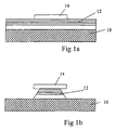
- Figure 1a shows a base plate, constituting a substrate 10, coated of a stack of layer 12 which, after different operations will form the laser waveguide, consisting of an active region and two coats taking this last sandwich.
- the following operation consists in depositing the layer electrically insulating 22, while maintaining the masking layer 14.
- This operation is carried out by depositing InP in the vapor phase, by a chemical process, from an organometallic compound, better known to those skilled in the art under the abbreviation of MOCVD abbreviation of English paraphrase “metal organic physical vapor deposition. "Such a process is described in a manner complete in “Materials Aspects of GaAs and InP Based Srtuctures "by V. Swaminathan and A. T. Macrander, Prentice Hall advanced reference series. ISBN 0-13-346826-7.
- the deposit is interrupted when the thickness of the layer 22, of InP, is equal to that of stacking 12.
- the doped InP substrate provides the lower electrode function. Also, in applying a voltage between the two electrodes, it is possible to inject a current in the stack, to cause the emission of coherent light.
- the structure of the stack can, of course, also include numerous configuration variants, for example those described in patent applications WO 99/00572 and FR 99 03845.
Abstract
Description
La présente invention concerne les lasers semi-conducteurs à cascade quantique. Dans la présente demande, on entend par laser semi-conducteur à cascade quantique un laser dans lequel le gain provient de porteurs effectuant des transitions inter-sous-bandes dans une hétérostructure de semi-conducteurs.The present invention relates to cascade semiconductor lasers Quantum. In the present application, the term semiconductor laser to quantum cascade a laser in which the gain comes from carriers performing inter-subband transitions in a semiconductor heterostructure.
Un laser de ce type est, par exemple, décrit dans le document intitulé "Buried heterostructure quantum cascade lasers", publié dans SPIE Vol. 3284 0277-786X98. Sa structure et le procédé de fabrication mis en oeuvre seront expliqués de manière détaillée dans la description qui va suivre, en référence à la figure 1,A laser of this type is, for example, described in the document entitled "Buried quantum heterostructure cascade lasers ", published in SPIE Vol 3284 0277-786X98. Its structure and the manufacturing process implemented will be explained in detail in the description which follows, with reference in Figure 1,
De tels lasers comportent un substrat en phosphure d'indium (InP). dopé au silicium, sur lequel est disposé un empilement de couches très minces formant le guide d'onde du laser. L'empilement a une structure prismatique, de section sensiblement trapézoïdale, dont la face inférieure, qui forme la grande base du trapèze, repose sur le substrat.Such lasers comprise an indium phosphide (InP) substrate. doped silicon, on which is arranged a stack of very thin layers forming the waveguide of the laser. The stack has a prismatic structure, substantially trapezoidal section, whose lower face, which forms the large trapezium base, rests on the substrate.
Les faces inférieure et supérieure sont formées chacune par des couches d'alliages d'arséniure d'indium et de gallium (InGaAs), et d'arséniure d'indium et d'aluminium (AlInAs) constituant un manteau.The lower and upper faces are each formed by layers alloys of indium gallium arsenide (InGaAs) and indium arsenide and aluminum (AlInAs) constituting a mantle.
Une succession de couches d'arséniure d'aluminium et d'indium (AlInAs) et d'arséniure d'indium et de gallium (InGaAs) forme la région active du laser, qui est disposée entre les deux manteaux.A succession of layers of aluminum arsenide and indium (AlInAs) and of indium gallium arsenide (InGaAs) forms the active region of the laser, which is arranged between the two coats.
Pour assurer l'injection d'un courant électrique dans la région active, le laser comporte, en outre, deux électrodes. La première électrode est formée par le substrat. La seconde est réalisée au moyen d'une couche métallique disposée par-dessus le substrat et en contact sur, au moins, une partie de la face supérieure de l'empilement. Une couche électriquement isolante, en InP, supporte la couche métallique, à l'exception de la zone de contact. To ensure the injection of an electric current into the active region, the laser comprises, in addition, two electrodes. The first electrode is formed by the substrate. The second is made by means of a metal layer arranged over the substrate and in contact with at least part of the face top of the stack. An electrically insulating layer, in InP, supports the metal layer, with the exception of the contact area.
La fabrication d'un tel laser fait appel à un substrat en InP dopé, de manière à le rendre conducteur, pour former la première électrode. Des couches successives sont ensuite déposées, qui constituent l'empilement. Ces couches sont alors attaquées, de manière classique, par photolithographie. On obtient ainsi la structure prismatique de section trapézoïdale.The manufacture of such a laser uses a doped InP substrate, so as to make it conductive, to form the first electrode. Layers successive are then deposited, which constitute the stack. These The layers are then etched in a conventional manner by photolithography. This gives the prismatic structure of trapezoidal section.
L'ensemble ainsi obtenu est recouvert, par épitaxie par jet moléculaire, d'une couche de InP revêtant toute la face supérieure du dispositif à ce stade de la fabrication. Une nouvelle opération de photolithographie permet de pratiquer une ouverture dans la zone recouvrant la face supérieure de l'empilement. Les bords de l'ouverture, constitués par la tranche de la couche électriquement isolante, forment ainsi un puits au fond duquel se trouve la face supérieure de l'empilement. La couche métallique, par exemple du chrome, est ensuite déposée sur la couche électriquement isolante ainsi que sur la face supérieure de l'empilement, pour former la seconde électrode.The assembly thus obtained is covered, by molecular beam epitaxy, with a layer of InP coating the entire upper face of the device at this stage of the manufacturing. A new photolithography operation makes it possible to practice an opening in the area covering the upper face of the stack. The edges of the opening, constituted by the edge of the layer electrically insulating, thus forming a well at the bottom of which is the upper face of the stack. The metal layer, for example chromium, is then deposited on the electrically insulating layer and on the upper face of the stack, to form the second electrode.
En appliquant une tension électrique entre les faces inférieure et supérieure de l'empilement, soit entre les deux électrodes, on y injecte un courant électrique qui engendre le rayonnement laser.By applying an electrical voltage between the lower and upper faces of the stack, or between the two electrodes, a current is injected which generates the laser radiation.
Ces lasers ont pour avantage de pouvoir être construits pour opérer dans une grande partie du spectre infrarouge moyen (de 3 à 20 µm de longueur d'onde environ) en utilisant les mêmes matériaux semi-conducteurs de base.These lasers have the advantage of being able to be built to operate in a much of the average infrared spectrum (from 3 to 20 μm wavelength about) using the same basic semiconductor materials.
Des lasers présentant des structures similaires, auxquelles la présente invention peut être appliquée, ont été décrites, notamment, dans les demandes de brevets WO 99/00572 et FR 99 03845.Lasers with similar structures, to which this invention can be applied, have been described, in particular, in the patent applications WO 99/00572 and FR 99 03845.
Le fonctionnement de ces lasers dépend considérablement de la température de l'empilement lors de l'émission. Or, lorsque le laser est activé, une part sensible de l'énergie se transforme en chaleur. Celle-ci est essentiellement dissipée par diffusion dans le substrat. La dissipation est relativement lente, ce qui limite donc considérablement les conditions d'utilisation.The operation of these lasers depends greatly on the temperature stacking during the show. However, when the laser is activated, a part Sensitive energy turns into heat. This one is essentially dissipated by diffusion in the substrate. The dissipation is relatively slow, which therefore considerably limits the conditions of use.
Dans le dispositif réalisé comme décrit ci-dessus, il est avantageux que la couche électriquement isolante soit aussi épaisse que possible, car l'InP est un bon conducteur thermique. Cela permet d'éviter une élévation exagérée de la température. Malheureusement, plus la couche est épaisse, plus il est difficile de maítriser l'attaque en vue de former la découpe destinée à permettre le contact électrique entre l'électrode et la face supérieure de l'empilement.In the device produced as described above, it is advantageous for the electrically insulating layer is as thick as possible because the InP is a good thermal conductor. This avoids an exaggerated rise in temperature. Unfortunately, the thicker the layer, the more difficult to master the attack in order to form the cut destined to allow the electrical contact between the electrode and the upper face of stacking.
En outre, le dépôt de l'InP par épitaxie par jet moléculaire nécessite une opération de nettoyage sous ultra-vide, ce qui est délicat et coûteux.In addition, the deposition of InP by molecular beam epitaxy requires a cleaning operation under ultra-vacuum, which is delicate and expensive.
Par ailleurs, la fonction d'isolation repose sur la qualité d'une barrière Schottky, ce qui est également difficile à maítriser.In addition, the insulation function is based on the quality of a barrier Schottky, which is also difficult to master.
Le but de la présente invention est de permettre la réalisation de lasers dans lesquels la couche électriquement isolante assure une dissipation optimale de la température, de manière reproductible et à un coût raisonnable.The purpose of the present invention is to enable the production of lasers in which the electrically insulating layer ensures optimal dissipation of temperature, reproducibly and at a reasonable cost.
Ce but est atteint grâce au fait que la couche électriquement isolante recouvre totalement lesdites faces latérales, sans déborder sur la face supérieure, et en ce que son épaisseur est égale à au moins un tiers de l'épaisseur de l'empilement. Une telle épaisseur est suffisante pour permettre une bonne diffusion thermique.This goal is achieved thanks to the fact that the electrically insulating layer covers totally said lateral faces, without overflowing on the upper face, and its thickness is equal to at least a third of the thickness of stacking. Such a thickness is sufficient to allow a good thermal diffusion.
Bien que l'empilement soit de faible épaisseur, il forme une protubérance qui fait que l'ensemble présente une structure non planaire. De la sorte, le laser ne peut être fixé sur un support que par son substrat. Or, un montage du laser, indifféremment sur l'une ou l'autre face, simplifie les opérations d'assemblage. Dans les cas où la dissipation thermique joue un grand rôle, il est avantageux de disposer d'un support fortement conducteur de la chaleur, en contact direct avec la couche électriquement isolante . C'est pourquoi, dans un mode particulier de réalisation, la couche électriquement isolante recouvre le substrat au moins dans la zone attenante à l'empilement et présente une épaisseur au moins égale à celle de l'empilement.Although the stack is thin, it forms a protuberance which fact that the set has a non-planar structure. In this way, the laser can be fixed on a support only by its substrate. Now, a montage of the laser, indifferently on one or the other side, simplifies the operations assembly. In cases where heat dissipation plays a large role, is advantageous to have a support highly conducive to heat, in direct contact with the electrically insulating layer. That is why, in a particular embodiment, the electrically insulating layer covers the substrate at least in the area adjacent to the stack and has a thickness at least equal to that of the stack.
De manière avantageuse, l'épaisseur de la couche électriquement isolante est égale à celle de l'empilement. Il est toutefois envisageable, pour certaines applications, de réaliser une couche électriquement isolante dont l'épaisseur est supérieure à celle de l'empilement. Dans ce cas également, la diffusion thermique est améliorée et la planéité de la deuxième face assurée.Advantageously, the thickness of the electrically insulating layer is equal to that of the stack. However, it is possible for some applications, to produce an electrically insulating layer whose thickness is greater than that of the stack. In this case too, the diffusion Thermal is improved and the flatness of the second face ensured.
Dans un mode de réalisation particulièrement avantageux, le substrat est en matériau semi-conducteur dopé pour le rendre conducteur.In a particularly advantageous embodiment, the substrate is in semiconductor material doped to make it conductive.
Parmi les différents types de lasers semi-conducteurs à cascade quantique, ceux présentant les caractéristiques suivantes ont donné des résultats particulièrement bons:
- le substrat est formé d'une plaque en phosphure d'indium (InP), dopé au silicium,
- les manteaux sont formés chacun par des couches en un alliage d'arséniure d'indium et de gallium (InGaAs) et un alliage d'arséniure d'indium et d'aluminium,
- la région active est formée d'une succession de couches d'arséniure d'aluminium et d'indium (AlInAs) et d'arséniure d'indium et de gallium (InGaAs), et
- la couche électriquement isolante est en InP.
- the substrate is formed of an indium phosphide plate (InP) doped with silicon,
- the coats are each formed by layers of an indium gallium arsenide alloy (InGaAs) and an indium aluminum arsenide alloy,
- the active region is formed of a series of layers of aluminum arsenide and indium (AlInAs) and indium gallium arsenide (InGaAs), and
- the electrically insulating layer is InP.
Dans une première variante, le phosphure d'indium formant la couche électriquement isolante est de type semi-isolant, par dopage au fer.In a first variant, the indium phosphide forming the layer electrically insulating is of semi-insulating type, by doping with iron.
Dans une autre variante, le phosphure d'indium formant la couche électriquement isolante est de type non dopé.In another variant, the indium phosphide forming the layer electrically insulating is undoped type.
La présente invention concerne également un procédé de fabrication d'un laser tel que décrit ci-dessus. Des résultats particulièrement intéressants ont été obtenus en appliquant un procédé comportant les opérations suivantes:
- dépôt des couches destinées à former l'empilement,
- dépôt d'une couche de masquage,
- attaque de la couche de masquage en dehors de la zone destinée à former l'empilement,
- attaque des couches destinées à former l'empilement en dehors de la zone masquée,
- dépôt en phase vapeur par procédé chimique à partir d'un composé organométallique (MOCVD) d'une couche électriquement isolante sur les parties non masquées, jusqu'à atteindre une épaisseur au moins égale au tiers de l'épaisseur de l'empilement,
- élimination de la couche de masquage, et
- dépôt d'une couche conductrice, recouvrant notamment l'empilement sur sa face supérieure.
- deposition of the layers intended to form the stack,
- depositing a masking layer,
- attacking the masking layer outside the zone intended to form the stack,
- attacking layers intended to form the stack outside the masked area,
- chemical vapor deposition from an electrically insulating layer on an unmasked part of an organometallic compound (MOCVD) to a thickness at least equal to one third of the thickness of the stack,
- removal of the masking layer, and
- deposition of a conductive layer, covering in particular the stack on its upper face.
Comme seule la face supérieure du prisme est masquée, il en résulte que les faces latérales sont entièrement couvertes par la couche électriquement isolante alors que la face supérieure est totalement épargnée.As only the upper face of the prism is masked, it follows that the side faces are fully covered by the electrically layer insulation while the upper face is completely spared.
De manière avantageuse, l'opération de dépôt de la couche électriquement isolante s'effectue jusqu'à atteindre une épaisseur sensiblement égale à l'épaisseur de l'empilement.Advantageously, the operation of depositing the layer electrically insulation is carried out until a thickness substantially equal to the thickness of the stack.
Afin d'éviter que la couche de matériau isolant ne se dépose sur la couche de masquage, il est avantageux que celle-ci soit réalisée en dioxyde de silicium (SiO2).In order to prevent the layer of insulating material from being deposited on the masking layer, it is advantageous for it to be made of silicon dioxide (SiO 2 ).
D'autres avantages et caractéristiques de l'invention ressortiront de la description qui va suivre, faite en regard du dessin annexé, dans lequel:
- La figure 1 représente, de manière schématique, un laser correspondant à l'état de la technique, durant différentes étapes de sa fabrication; et
- La figure 2 montre, selon la même approche schématique, un laser selon l'invention à différents stades de sa fabrication.
- Figure 1 shows schematically a laser corresponding to the state of the art, during different stages of its manufacture; and
- FIG. 2 shows, according to the same schematic approach, a laser according to the invention at different stages of its manufacture.
Afin de faciliter la compréhension de l'invention, un laser de type connu, objet de l'article paru dans la revue SPIE, mentionné plus haut, sera donc décrit de manière succincte, en référence à la figure 1. Sur cette figure, les dimensions des différentes parties constitutives du laser sont choisies pour faciliter la lecture du dessin. Elles ne sont pas significatives des dimensions réelles. In order to facilitate the understanding of the invention, a known type of laser, object of the article published in SPIE, mentioned above, will therefore be succinctly, with reference to Figure 1. In this figure, the dimensions different parts of the laser are chosen to facilitate the reading the drawing. They are not significant of actual dimensions.
La figure 1a montre une plaque de base, constituant un substrat 10, revêtue
d'un empilement de couche 12 qui, après différentes opérations formeront le
guide d'onde du laser, constitué d'une région active et de deux manteaux
prenant cette dernière en sandwich.Figure 1a shows a base plate, constituting a
L'empilement 12 porte une couche de masquage 14, la recouvrant localement
dans la zone devant être épargnée.
De manière classique, le substrat 10 est réalisé au moyen d'une plaque en
monocristal de phosphure d'indium (InP) dopé au silicium. L'empilement 12
est formée d'une alternance de couches d'arséniure d'aluminium et d'indium
(AlInAs) et d'arséniure d'indium et de gallium (InGaAs), qui constituent deux
manteaux et une région active.Conventionally, the
La couche de masquage 14 est en dioxyde de silicium (SiO2), déposée
initialement sur toute la surface, les parties devant être éliminées l'étant par
photolithographie. En variante, il est aussi possible de réaliser directement la
couche de masquage au moyen de la résine utilisée dans le procédé de
photolithographie.The
L'ensemble ainsi obtenu est ensuite soumis à une attaque chimique, qui
élimine les couches formant l'empilement, à l'exception de la zone masquée.
Comme le montre la figure 1b, l'empilement 12 prend alors la forme d'un
prisme à section sensiblement trapézoïdale, dont la grande base est en
contact avec le substrat 10 et la petite base est recouverte par la couche de
masquage 14. Cette dernière est ensuite éliminée, pour obtenir la structure
représentée sur la figure 1c. La forme de la section du prisme est définie par
les moyens utilisés lors de l'attaque des couches formant l'empilement dans
les zones non masquées. Elle n'influence pas le fonctionnement du laser.The assembly thus obtained is then subjected to a chemical attack, which
eliminates the layers forming the stack, with the exception of the masked area.
As shown in FIG. 1b, the
Lors de l'opération suivante, illustrée à la figure 1d, toute la surface est
recouverte d'une couche électriquement isolante 16 de InP, par épitaxie par
jet moléculaire. Cette couche peut être réalisée au moyen de InP aussi pur
que possible, c'est-à-dire non dopée. Il est aussi possible d'utiliser de l'InP
dopé au fer, pour obtenir une couche de matériau appelé communément
semi-isolant, comme décrit dans la publication mentionnée plus haut.In the following operation, illustrated in Figure 1d, the entire surface is
covered with an electrically insulating
La couche 16 est, ensuite, localement attaquée, par photolithographie, pour
dégager une ouverture 18 dans la partie recouvrant la face supérieure de
l'empilement. Le tout est, ensuite, recouvert d'une couche en matériau
conducteur formant une électrode 20, par exemple du chrome, comme
représenté sur la figure 1e.The
Dans le dispositif réalisé comme décrit ci-dessus, il est avantageux que la couche électriquement isolante soit aussi épaisse que possible, car l'InP est un bon conducteur thermique. Il est ainsi possible d'éviter une élévation exagérée de la température. Malheureusement, plus la couche est épaisse, plus il est difficile de maítriser l'attaque en vue de former la découpe destinée à permettre le contact électrique entre l'électrode et la face supérieure de l'empilement.In the device produced as described above, it is advantageous for the electrically insulating layer is as thick as possible because the InP is a good thermal conductor. It is thus possible to avoid an elevation exaggerated temperature. Unfortunately, the thicker the layer, the more difficult it is to control the attack in order to form the cutout intended to allow electrical contact between the electrode and the upper face of stacking.
Le dépôt de l'InP par épitaxie par jet moléculaire nécessite une opération de nettoyage sous ultra-vide, ce qui est délicat et coûteux.Deposition of InP by molecular beam epitaxy requires an cleaning under ultra-vacuum, which is delicate and expensive.
Par ailleurs la fonction d'isolation repose sur la qualité d'une barrière Schottky, ce qui est également difficile à maítriser.In addition, the insulation function is based on the quality of a Schottky barrier, which is also difficult to master.
Enfin, bien que l'empilement soit de faible épaisseur, il forme une protubérance qui fait que l'ensemble présente une structure non-planaire. De ce fait, le substrat ne peut être fixé sur un support que par sa face opposée à celle portant l'empilement.Finally, although the stack is thin, it forms a protrusion that makes the whole has a non-planar structure. Of this fact, the substrate can be fixed on a support only by its opposite face to the one carrying the stack.
Si l'on se réfère à la figure 2, on constate que, dans le procédé selon
l'invention, les opérations représentées aux figures 1a et 1b se retrouvent à
l'identique sur les figures 2a et 2b, avec un substrat 10, un empilement 12 et
un couche de masquage 14.With reference to FIG. 2, it can be seen that in the process according to
the invention, the operations shown in FIGS. 1a and 1b are found in FIG.
identical in FIGS. 2a and 2b, with a
L'opération suivante, illustrée à la figure 2c, consiste à déposer la couche
électriquement isolante 22, en conservant la couche de masquage 14. Cette
opération s'effectue par dépôt de InP en phase vapeur, par procédé chimique,
à partir d'un composé organométallique, plus connu par l'homme du métier
sous l'abréviation de MOCVD abréviation de la périphrase anglaise "metal
organic physical vapor deposition". Un tel procédé est décrit de manière
complète dans l'ouvrage intitulé "Materials Aspects of GaAs and InP Based
Srtuctures" de V. Swaminathan et A. T. Macrander, Prentice Hall advanced
reference series. ISBN 0-13-346826-7.The following operation, illustrated in Figure 2c, consists in depositing the layer
electrically insulating 22, while maintaining the
Ce procédé permet le dépôt de couches relativement épaisses, recouvrant
totalement les faces latérales du prisme jusqu'au contact de la couche de
masquage 14. De la sorte, la couche électriquement isolante ne peut
déborder sur la face supérieure du prisme. De manière avantageuse, le dépôt
est interrompu au moment où l'épaisseur de la couche 22, de InP, est égale à
celle de l'empilement 12.This process allows the deposition of relatively thick layers, covering
totally the lateral faces of the prism until contact with the
14. In this way, the electrically insulating layer can not
overflow on the upper face of the prism. Advantageously, the deposit
is interrupted when the thickness of the
Comme on peut le voir sur la figure 2d, la couche de masquage 14 est ensuite
éliminée, puis une couche conductrice 24, par exemple en chrome, est
déposée, formant une électrode supérieure de contact.As can be seen in FIG. 2d, the
Le substrat en InP dopé assure la fonction d'électrode inférieure. Aussi, en appliquant une tension entre les deux électrodes, il est possible d'injecter un courant dans l'empilement, pour provoquer l'émission de lumière cohérente.The doped InP substrate provides the lower electrode function. Also, in applying a voltage between the two electrodes, it is possible to inject a current in the stack, to cause the emission of coherent light.
Il est aussi possible de réaliser une couche électriquement isolante 22
sensiblement plus épaisse que l'empilement 12. Dans ce cas, la face
supérieure du prisme se trouvera au fond d'une gorge. Une telle structure
permet aussi d'assurer une bonne diffusion thermique. Comme la surface de
la face supérieure du prisme est faible par rapport à la surface totale du
substrat, l'ensemble ainsi obtenu se présente sous forme d'une plaque dont
les deux faces sont planes et parallèles, l'une de ces dernières comportant
une gorge au droit de l'empilement.It is also possible to produce an electrically insulating
Il va de soi qu'il est possible de réaliser plusieurs lasers sur un même substrat. Ce dernier peut, ensuite, être découpé en plaquettes, chacune d'elles comportant un ou plusieurs lasers. Ces plaquettes sont disposées sur un support portant également des circuits électroniques de commande, destinés à assurer l'alimentation du laser. It goes without saying that it is possible to make several lasers on the same substrate. The latter can then be cut into platelets, each of them having one or more lasers. These pads are arranged on a support also carrying electronic control circuits, intended to provide power to the laser.
Il est évident que de nombreuses variantes peuvent être envisagées sans pour autant sortir du cadre de l'invention. Ainsi, il est également possible d'utiliser un substrat en matériau isolant, recouvert d'une couche conductrice, cette dernière assurant la fonction d'électrode.It is obvious that many variants can be envisaged without however, outside the scope of the invention. So, it is also possible to use a substrate of insulating material, covered with a conductive layer, the latter providing the function of electrode.
La structure de l'empilement peut, bien entendu, aussi comporter de nombreuses variantes de configurations, par exemples celles décrites dans les demandes de brevet WO 99/00572 et FR 99 03845.The structure of the stack can, of course, also include numerous configuration variants, for example those described in patent applications WO 99/00572 and FR 99 03845.
Claims (10)
- Quantum cascade semiconductor laser, comprising:characterized in that the said electrically insulating layer (22) completely covers the said lateral faces, without extending onto the upper face, and in that its thickness is equal to at least one third of the thickness of the multilayer (12).a substrate (10),a multilayer (12), of prismatic shape having an approximately trapezoidal cross section, with a lower face placed on the substrate (10), an upper face and lateral faces, the said multilayer forming a gain region and two claddings between which the gain region is interposed,two electrodes (10, 24) placed on either side of the multilayer (12), one (24) of which is formed by a layer of electrically conducting material at least partly covering that face of the multilayer on the opposite side from the substrate andan electrically insulating layer (22) interposed between the two electrodes,
- Laser according to Claim 1, characterized in that the said electrically insulating layer (22) covers the said substrate (10) at least in the zone contiguous with the said multilayer (12) and has a thickness at least equal to that of the latter.
- Laser according to Claim 2, characterized in that the thickness of the electrically insulating layer (22) is substantially equal to the thickness of the multilayer (12).
- Laser according to Claim 3, characterized in that the said substrate (10) is made of a semiconductor material doped to make it conducting.
- Laser according to Claim 4, characterized in that:the said substrate (10) is formed from a plate made of silicon-doped indium phosphide (InP),the said claddings are each formed by layers formed from an indium gallium arsenide alloy (InGaAs) and from an indium aluminium arsenide alloy,the active region is formed from a succession of aluminium indium arsenide (AlInAs) and indium gallium arsenide (InGaAs) layers and in thatthe said electrically insulating layer (22) is made of indium phosphide.
- Laser according to Claim 5, characterized in that the indium phosphide forming the electrically insulating layer (22) is of the iron-doped semiinsulating type.
- Laser according to Claim 5, characterized in that the indium phosphide forming the electrically insulating layer (22) is undoped.
- Process for manufacturing a laser according to one of the preceding claims, characterized in that it comprises the following steps:deposition of the layers intended to form the said multilayer (12);deposition of a masking layer (14);etching of the masking layer (14) outside the zone intended for form the said multilayer;etching of the layers intended to form the multilayer (12) outside the masked zone;metal oxide chemical vapour deposition (MOCVD) of an electrically insulating layer (22) on the unmasked parts until a thickness substantially equal to the thickness of the multilayer (12) is attained;removal of the masking layer (14); anddeposition of a conducting layer (24), covering in particular the multilayer (12) on its upper face.
- Process according to Claim 8, characterized in that the operation of depositing the electrically insulating layer (22) is carried out until a thickness substantially equal to the thickness of the multilayer (12) is attained.
- Process according to either of Claims 8 and 9, characterized in that the said masking layer (14) is made of SiO2.
Priority Applications (1)
| Application Number | Priority Date | Filing Date | Title |
|---|---|---|---|
| EP01905566A EP1262003B1 (en) | 2000-03-03 | 2001-02-26 | Quantum cascade laser and method for making same |
Applications Claiming Priority (4)
| Application Number | Priority Date | Filing Date | Title |
|---|---|---|---|
| EP00810183 | 2000-03-03 | ||
| EP00810183A EP1130724A1 (en) | 2000-03-03 | 2000-03-03 | Quantum cascade laser and method of manufacturing the same |
| PCT/CH2001/000123 WO2001065651A1 (en) | 2000-03-03 | 2001-02-26 | Quantum cascade laser and method for making same |
| EP01905566A EP1262003B1 (en) | 2000-03-03 | 2001-02-26 | Quantum cascade laser and method for making same |
Publications (2)
| Publication Number | Publication Date |
|---|---|
| EP1262003A1 EP1262003A1 (en) | 2002-12-04 |
| EP1262003B1 true EP1262003B1 (en) | 2003-11-12 |
Family
ID=8174582
Family Applications (2)
| Application Number | Title | Priority Date | Filing Date |
|---|---|---|---|
| EP00810183A Withdrawn EP1130724A1 (en) | 2000-03-03 | 2000-03-03 | Quantum cascade laser and method of manufacturing the same |
| EP01905566A Expired - Lifetime EP1262003B1 (en) | 2000-03-03 | 2001-02-26 | Quantum cascade laser and method for making same |
Family Applications Before (1)
| Application Number | Title | Priority Date | Filing Date |
|---|---|---|---|
| EP00810183A Withdrawn EP1130724A1 (en) | 2000-03-03 | 2000-03-03 | Quantum cascade laser and method of manufacturing the same |
Country Status (5)
| Country | Link |
|---|---|
| US (2) | US6665325B2 (en) |
| EP (2) | EP1130724A1 (en) |
| JP (1) | JP2003526214A (en) |
| DE (1) | DE60101217T2 (en) |
| WO (1) | WO2001065651A1 (en) |
Families Citing this family (19)
| Publication number | Priority date | Publication date | Assignee | Title |
|---|---|---|---|---|
| US6449024B1 (en) | 1996-01-26 | 2002-09-10 | Semiconductor Energy Laboratory Co., Inc. | Liquid crystal electro-optical device utilizing a polymer with an anisotropic refractive index |
| EP1283571B1 (en) | 2001-08-06 | 2015-01-14 | nanoplus GmbH Nanosystems and Technologies | Laser with weakly coupled grating |
| ATE361565T1 (en) * | 2002-03-08 | 2007-05-15 | Nanoplus Gmbh Nanosystems And | A SEMICONDUCTOR LASER ARRAY WITH SIDE GRATING STRUCTURE |
| US7301977B2 (en) * | 2004-06-10 | 2007-11-27 | Nanoplus Gmbh | Tuneable unipolar lasers |
| US7274719B2 (en) * | 2005-03-09 | 2007-09-25 | Agilent Technologies, Inc. | Buried heterostructure quantum cascade laser |
| US7403552B2 (en) * | 2006-03-10 | 2008-07-22 | Wisconsin Alumni Research Foundation | High efficiency intersubband semiconductor lasers |
| JP2008218915A (en) * | 2007-03-07 | 2008-09-18 | Hamamatsu Photonics Kk | Quantum cascade laser element |
| JP5355599B2 (en) * | 2011-01-19 | 2013-11-27 | 株式会社東芝 | Semiconductor light emitting device and manufacturing method thereof |
| JP5729138B2 (en) * | 2011-05-30 | 2015-06-03 | 住友電気工業株式会社 | Manufacturing method of optical semiconductor device |
| JP5803366B2 (en) * | 2011-07-14 | 2015-11-04 | 住友電気工業株式会社 | Method of manufacturing buried heterostructure semiconductor laser and buried heterostructure semiconductor laser |
| JP2013149665A (en) | 2012-01-17 | 2013-08-01 | Sumitomo Electric Ind Ltd | Quantum cascade semiconductor laser |
| JP2013254907A (en) | 2012-06-08 | 2013-12-19 | Sumitomo Electric Ind Ltd | Quantum cascade semiconductor laser |
| JP2014229744A (en) * | 2013-05-22 | 2014-12-08 | 住友電気工業株式会社 | Semiconductor light-emitting assembly |
| JP6467193B2 (en) * | 2014-10-30 | 2019-02-06 | 浜松ホトニクス株式会社 | Quantum cascade laser |
| CN107251346B (en) | 2014-12-03 | 2020-08-28 | 阿尔佩斯激光有限公司 | Quantum cascade laser with current blocking layer |
| CN107408790B (en) * | 2014-12-19 | 2020-09-11 | 阿尔佩斯激光有限公司 | Quantum cascade laser optimized for epitaxial lateral downward mounting |
| JP6464895B2 (en) | 2015-04-03 | 2019-02-06 | 住友電気工業株式会社 | Quantum cascade laser diode |
| JP2016197657A (en) | 2015-04-03 | 2016-11-24 | 住友電気工業株式会社 | Quantum cascade semiconductor laser |
| JP2017157865A (en) * | 2017-06-07 | 2017-09-07 | 株式会社東芝 | Semiconductor light-emitting device and method of manufacturing the same |
Family Cites Families (18)
| Publication number | Priority date | Publication date | Assignee | Title |
|---|---|---|---|---|
| JPS62166586A (en) * | 1986-01-20 | 1987-07-23 | Nec Corp | Semiconductor light emitting element and manufacture thereof |
| JP2747080B2 (en) * | 1990-03-26 | 1998-05-06 | 松下電器産業株式会社 | Semiconductor laser device and method of manufacturing the same |
| US5214662A (en) * | 1990-11-16 | 1993-05-25 | Furukawa Electric Co., Ltd. | Semiconductor optical devices with pn current blocking layers of wide-band gap materials |
| JP2814786B2 (en) * | 1991-10-08 | 1998-10-27 | 日本電気株式会社 | Semiconductor laser |
| US5416790A (en) * | 1992-11-06 | 1995-05-16 | Sanyo Electric Co., Ltd. | Semiconductor laser with a self-sustained pulsation |
| DE4314498A1 (en) * | 1993-05-03 | 1994-11-10 | Bayer Ag | Process for the preparation of perfluoroalkoxy (alkylthio) benzenes |
| JPH07193333A (en) | 1993-12-27 | 1995-07-28 | Mitsubishi Chem Corp | Semiconductor light-emitting element |
| US5400354A (en) * | 1994-02-08 | 1995-03-21 | Ludowise; Michael | Laminated upper cladding structure for a light-emitting device |
| JPH07254750A (en) * | 1994-03-15 | 1995-10-03 | Toshiba Corp | Semiconductor laser |
| US5789772A (en) * | 1994-07-15 | 1998-08-04 | The Whitaker Corporation | Semi-insulating surface light emitting devices |
| JPH09331110A (en) * | 1996-06-12 | 1997-12-22 | Mitsubishi Electric Corp | Optical semiconductor device and manufacture thereof |
| JP3684519B2 (en) * | 1996-08-20 | 2005-08-17 | 富士通株式会社 | Semiconductor laser manufacturing method |
| US5789722A (en) * | 1996-11-12 | 1998-08-04 | Zimac Laboratories, Inc. | Modular multizone heater system and method |
| GB9704987D0 (en) * | 1997-03-11 | 1997-04-30 | Isis Innovation | Infrared radiation source |
| JPH11121860A (en) * | 1997-10-20 | 1999-04-30 | Oki Electric Ind Co Ltd | Compound semiconductor light emitting device and its forming method |
| US6137817A (en) * | 1998-06-12 | 2000-10-24 | Lucent Technologies Inc. | Quantum cascade laser |
| US6556605B1 (en) * | 2000-02-29 | 2003-04-29 | Triquent Technology Holding, Co. | Method and device for preventing zinc/iron interaction in a semiconductor laser |
| US6463088B1 (en) * | 2000-07-07 | 2002-10-08 | Lucent Technologies Inc. | Mesa geometry semiconductor light emitter having chalcogenide dielectric coating |
-
2000
- 2000-03-03 EP EP00810183A patent/EP1130724A1/en not_active Withdrawn
-
2001
- 2001-02-26 DE DE60101217T patent/DE60101217T2/en not_active Expired - Lifetime
- 2001-02-26 JP JP2001564428A patent/JP2003526214A/en active Pending
- 2001-02-26 EP EP01905566A patent/EP1262003B1/en not_active Expired - Lifetime
- 2001-02-26 US US10/220,099 patent/US6665325B2/en not_active Expired - Lifetime
- 2001-02-26 WO PCT/CH2001/000123 patent/WO2001065651A1/en active IP Right Grant
-
2003
- 2003-12-15 US US10/736,488 patent/US20040126912A1/en not_active Abandoned
Also Published As
| Publication number | Publication date |
|---|---|
| JP2003526214A (en) | 2003-09-02 |
| EP1130724A1 (en) | 2001-09-05 |
| US20030021315A1 (en) | 2003-01-30 |
| US20040126912A1 (en) | 2004-07-01 |
| DE60101217T2 (en) | 2004-09-09 |
| EP1262003A1 (en) | 2002-12-04 |
| US6665325B2 (en) | 2003-12-16 |
| WO2001065651A1 (en) | 2001-09-07 |
| DE60101217D1 (en) | 2003-12-18 |
Similar Documents
| Publication | Publication Date | Title |
|---|---|---|
| EP1262003B1 (en) | Quantum cascade laser and method for making same | |
| EP0829934B1 (en) | Method of fabricating an optoelectrical semiconductor device and a device or matrix of devices fabricated using said method | |
| EP3168946B1 (en) | Laser device and method for manufacturing such a laser device | |
| EP3352312B1 (en) | Photonic device including a laser optically connected to a silicon waveguide and method for manufacturing such a photonic device | |
| EP0765014B1 (en) | Surface emitting vertical cavity laser with a wavelength between 1,3 and 1,5 micrometer and its realisation | |
| FR2690278A1 (en) | Multispectral photovoltaic component with cell stack, and production method. | |
| FR2695261A1 (en) | Surface emission laser with current narrowed layer - has narrowed layer material with forbidden band width larger than that of active region and adjacent cladding layer. | |
| FR2727791A1 (en) | OPTICAL SEMICONDUCTOR DEVICE AND METHOD OF MANUFACTURING THE SAME | |
| EP0617839B1 (en) | Method of making semiconductor components, in particular on GaAs or InP, with recovery of the substrate by chemical means | |
| FR2967813A1 (en) | METHOD FOR PRODUCING A BENTALLIC METAL LAYER STRUCTURE | |
| FR2690286A1 (en) | Laser cavity with asymmetrical semi-conductor heterostructure and laser equipped with this cavity. | |
| EP2504895B1 (en) | Laser emission system, heterostructure and active zone comprising coupled sub-quantumwells, use for a laser emiission at 1.55 micrometers | |
| EP0817337B1 (en) | Method of fabricating a surface emitting laser | |
| FR2761811A1 (en) | ENGRAVING-FREE TECHNOLOGY FOR INTEGRATING COMPONENTS | |
| EP1670066A1 (en) | Fabrication method for an integrated circuit including a buried mirror and such circuit | |
| EP0494013A1 (en) | Method of manufacturing surface emitting semiconductor lasers and lasers obtained thereby | |
| EP1470622B1 (en) | Saturable absorber component and method for production of a saturable absorber component | |
| EP1618611A1 (en) | Method for production of a semiconductor device with auto-aligned metallisations | |
| FR2701574A1 (en) | Semiconductor modulator of light intensity. | |
| FR2743197A1 (en) | SEMICONDUCTOR DEVICE WITH MESA STRUCTURE AND METHOD OF MANUFACTURING SUCH A DEVICE | |
| EP0506557B1 (en) | Method of producing a buried-stripe type semiconductor laser device | |
| EP0689253A1 (en) | Process for producing an array of electrically driven quantum well components having a vertical structure | |
| EP0498695B1 (en) | Method of producing a planar stripe-buried semiconductor laser | |
| EP0617841B1 (en) | Method of making semiconductor components with recovery of the substrate by electrochemical means | |
| FR2485823A1 (en) | SEMICONDUCTOR LASER |
Legal Events
| Date | Code | Title | Description |
|---|---|---|---|
| PUAI | Public reference made under article 153(3) epc to a published international application that has entered the european phase |
Free format text: ORIGINAL CODE: 0009012 |
|
| 17P | Request for examination filed |
Effective date: 20020904 |
|
| AK | Designated contracting states |
Kind code of ref document: A1 Designated state(s): AT BE CH CY DE DK ES FI FR GB GR IE IT LI LU MC NL PT SE TR |
|
| RIN1 | Information on inventor provided before grant (corrected) |
Inventor name: MULLER, ANTOINE Inventor name: BECK, MATTIAS Inventor name: FAIST,JEROME |
|
| GRAH | Despatch of communication of intention to grant a patent |
Free format text: ORIGINAL CODE: EPIDOS IGRA |
|
| GRAS | Grant fee paid |
Free format text: ORIGINAL CODE: EPIDOSNIGR3 |
|
| GRAA | (expected) grant |
Free format text: ORIGINAL CODE: 0009210 |
|
| AK | Designated contracting states |
Kind code of ref document: B1 Designated state(s): CH DE FR GB LI |
|
| REG | Reference to a national code |
Ref country code: GB Ref legal event code: FG4D Free format text: NOT ENGLISH |
|
| REG | Reference to a national code |
Ref country code: CH Ref legal event code: EP |
|
| REF | Corresponds to: |
Ref document number: 60101217 Country of ref document: DE Date of ref document: 20031218 Kind code of ref document: P |
|
| REG | Reference to a national code |
Ref country code: IE Ref legal event code: FG4D Free format text: FRENCH |
|
| REG | Reference to a national code |
Ref country code: CH Ref legal event code: NV Representative=s name: GLN GRESSET & LAESSER NEUCHATEL CABINET DE CONSEIL |
|
| GBT | Gb: translation of ep patent filed (gb section 77(6)(a)/1977) |
Effective date: 20040211 |
|
| REG | Reference to a national code |
Ref country code: IE Ref legal event code: FD4D |
|
| PLBE | No opposition filed within time limit |
Free format text: ORIGINAL CODE: 0009261 |
|
| STAA | Information on the status of an ep patent application or granted ep patent |
Free format text: STATUS: NO OPPOSITION FILED WITHIN TIME LIMIT |
|
| 26N | No opposition filed |
Effective date: 20040813 |
|
| PG25 | Lapsed in a contracting state [announced via postgrant information from national office to epo] |
Ref country code: FR Free format text: LAPSE BECAUSE OF NON-PAYMENT OF DUE FEES Effective date: 20051031 |
|
| REG | Reference to a national code |
Ref country code: FR Ref legal event code: ST Effective date: 20051031 |
|
| REG | Reference to a national code |
Ref country code: FR Ref legal event code: D3 |
|
| REG | Reference to a national code |
Ref country code: CH Ref legal event code: PFA Owner name: ALPES LASERS S.A., CH Free format text: FORMER OWNER: ALPES LASERS S.A., CH |
|
| REG | Reference to a national code |
Ref country code: FR Ref legal event code: PLFP Year of fee payment: 16 |
|
| REG | Reference to a national code |
Ref country code: CH Ref legal event code: PFA Owner name: ALPES LASERS S.A., CH Free format text: FORMER OWNER: ALPES LASERS S.A., CH |
|
| REG | Reference to a national code |
Ref country code: FR Ref legal event code: PLFP Year of fee payment: 17 |
|
| REG | Reference to a national code |
Ref country code: FR Ref legal event code: PLFP Year of fee payment: 18 |
|
| REG | Reference to a national code |
Ref country code: CH Ref legal event code: NV Representative=s name: BOVARD SA NEUCHATEL CONSEILS EN PROPRIETE INTE, CH |
|
| REG | Reference to a national code |
Ref country code: CH Ref legal event code: NV Representative=s name: ABACUS PATENTANWAELTE KLOCKE SPAETH BARTH, CH |
|
| PG25 | Lapsed in a contracting state [announced via postgrant information from national office to epo] |
Ref country code: FR Free format text: LAPSE BECAUSE OF NON-PAYMENT OF DUE FEES Effective date: 20051031 |
|
| PGRI | Patent reinstated in contracting state [announced from national office to epo] |
Ref country code: FR Effective date: 20060203 |
|
| PGFP | Annual fee paid to national office [announced via postgrant information from national office to epo] |
Ref country code: DE Payment date: 20191212 Year of fee payment: 20 Ref country code: GB Payment date: 20200219 Year of fee payment: 20 |
|
| PGFP | Annual fee paid to national office [announced via postgrant information from national office to epo] |
Ref country code: FR Payment date: 20200219 Year of fee payment: 20 |
|
| PGFP | Annual fee paid to national office [announced via postgrant information from national office to epo] |
Ref country code: CH Payment date: 20200427 Year of fee payment: 20 |
|
| REG | Reference to a national code |
Ref country code: DE Ref legal event code: R071 Ref document number: 60101217 Country of ref document: DE |
|
| REG | Reference to a national code |
Ref country code: CH Ref legal event code: PL |
|
| REG | Reference to a national code |
Ref country code: GB Ref legal event code: PE20 Expiry date: 20210225 |
|
| PG25 | Lapsed in a contracting state [announced via postgrant information from national office to epo] |
Ref country code: GB Free format text: LAPSE BECAUSE OF EXPIRATION OF PROTECTION Effective date: 20210225 |