EP1258841A2 - Magnetic sensor and bill validator using the same - Google Patents
Magnetic sensor and bill validator using the same Download PDFInfo
- Publication number
- EP1258841A2 EP1258841A2 EP02010180A EP02010180A EP1258841A2 EP 1258841 A2 EP1258841 A2 EP 1258841A2 EP 02010180 A EP02010180 A EP 02010180A EP 02010180 A EP02010180 A EP 02010180A EP 1258841 A2 EP1258841 A2 EP 1258841A2
- Authority
- EP
- European Patent Office
- Prior art keywords
- bill
- magnetic
- sensor
- lattice
- artificial
- Prior art date
- Legal status (The legal status is an assumption and is not a legal conclusion. Google has not performed a legal analysis and makes no representation as to the accuracy of the status listed.)
- Granted
Links
Images


Classifications
-
- G—PHYSICS
- G07—CHECKING-DEVICES
- G07D—HANDLING OF COINS OR VALUABLE PAPERS, e.g. TESTING, SORTING BY DENOMINATIONS, COUNTING, DISPENSING, CHANGING OR DEPOSITING
- G07D7/00—Testing specially adapted to determine the identity or genuineness of valuable papers or for segregating those which are unacceptable, e.g. banknotes that are alien to a currency
- G07D7/04—Testing magnetic properties of the materials thereof, e.g. by detection of magnetic imprint
Landscapes
- Physics & Mathematics (AREA)
- General Physics & Mathematics (AREA)
- Inspection Of Paper Currency And Valuable Securities (AREA)
- Investigating Or Analyzing Materials By The Use Of Magnetic Means (AREA)
- Measuring Magnetic Variables (AREA)
Abstract
Description
- The present invention relates to a bill validator for use in various kinds of automatic vending machines and ticket machines.
- In recent years, in connection with various kinds of expensive goods sold by automatic vending machines or ticket machines. For example, a bill validator capable of using currency bills of denominations above 1000 yen has been widely used in Japan. Since Japanese government began issuing a new currency bill of 2000 yen in July 2000, vending machines capable of using larger denomination bills including 2000 yen are becoming the standard. On the other hand, due to rapid technology advance in office automation equipment such as copying machines or color printers, violation crimes using forged bills made by such sophisticated tools is also increasing. A bill validator must be improved for highly sensitive validation to prevent such crimes from being committed.
- In prior art, a bill validator has used a conventional magnetic read head as a sensor to detect magnetic features of a bill. Such a magnetic read head, however, needs a direct contact to have adequate signals with high accuracy from a magnetic media. Therefore, reading of currency is more difficult to detect with high accuracy because magnetic fields exist on both the face and the back side of bill which has a certain paper thickness. The drawback is the difficulty of improvement in validation accuracy.
- A magnetic sensor and a bill validator using the magnetic sensor are disclosed. A magnetic sensor comprised of an artificial-lattice MR (magnetic resistor) element formed on a face of a board detects magnetic field features of a media passing close to the face of the board. The artificial-lattice MR element formed on the board and wiring terminals coupled to the artificial-lattice MR element are integrated in a housing with resin. Moreover, a magnet is mounted on the back of the board in the housing to provide a plane of artificial-lattice MR element with an auxiliary magnetic field perpendicularly.
- Fig. 1 is a cross-sectional side view of a magnetic sensor used in the first exemplary embodiment of the present invention.
- Fig. 2 is a cross-sectional view of an artificial-lattice MR element used in the first exemplary embodiment of the present invention.
- Fig. 3 is a plan view of a magnetic sensor used in the first exemplary embodiment of the present invention.
- Fig. 4 is a side view, partly broken away, of a magnetic-sensor-assembly covered by a case, used in the first exemplary embodiment of the present invention.
- Fig. 5 is a front view, partly broken away, of magnetic-sensor-assembly covered in a case, used in the first exemplary embodiment of the present invention.
- Fig. 6 is an assembling view of a magnetic-sensor-assembly, covered in a case, used in the first exemplary embodiment of the present invention.
- Fig. 7 is a cross-sectional view of a bill validator equipped with a magnetic-sensor-assembly used in the first exemplary embodiment of the present invention.
- Fig. 8 is a block diagram of a bill validator equipped with a magnetic sensor used in the first exemplary embodiment of the present invention.
- Fig. 9 is a signal diagram from a magnetic sensor in a bill validator shown in the first exemplary embodiment of the present invention.
- Fig. 10 is a signal output diagram from a sample-hold circuit of a bill validator shown in the first exemplary embodiment of the present invention.
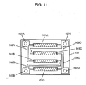
- Fig. 11 is a plan view of a magnetic sensor used in the second exemplary embodiment of the present invention.
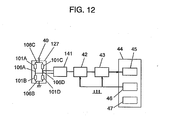
- Fig. 12 is a block diagram of a bill validator equipped with a magnetic sensor used in the second exemplary embodiment of the present invention.
- The present invention is explained by following preferred embodiments with reference to Fig. 1 through Fig. 12.
- Fig. 1 is a cross-sectional view of a magnetic sensor of the first exemplary embodiment. In Fig. 1, artificial-lattice MR (magnetic resistor)
element 1 is formed on surface ofceramic board 2. As shown in Fig. 2, artificial-lattice MR element has a multi-layer structure comprising nonmagnetic Copper (Cu)layers layers ceramic board 2 with surfaceprotective finish 5. - As described above, artificial-
lattice MR element 1, having a multi-layer structure ofnonmagnetic layers 3 andmagnetic layers 4 sandwiched alternately, shows a large change in electrical resistance of the multi-layer structure when a magnetic field is applied perpendicularly. The effect can be used for detecting a faint change in magnetic fields. - Etching the above-mentioned multi-layer artificial-lattice MR element forms a circuit configuration as shown in Fig. 3. Namely, coupling two artificial-
lattice MR element conductive pattern 6A, and both ends are connected topattern Patterns wiring terminals holes - As mentioned above, a simple circuit configuration can detect changes of magnetic fields, when two artificial-lattice MR elements, 1A and 1B, are arranged so that magnetic media passes in front of each artificial-lattice MR element, sequentially in the order of 1A to 1B.
- In Fig. 1,
wiring terminal 8, coupled to the artificial-lattice MR element to tap off signals, is disposed on the back ofboard 2.Terminal 8 is coupled to artificial-lattice MR element 1 via through-hole 7.Board 2 and one end ofwiring terminal 8 onboard 2 are sealed with resin, forming an integration inhousing 9.Magnet 11, fitting to approximately square-shaped hollow 10, opening downward, is mounted such that being embedded.Magnet 11, mounted on the back ofboard 2, provides artificial-lattice MR element 1 with auxiliary magnetic field perpendicularly. Strength of the auxiliary magnetic field is approximately 20 milliTesla (mT). An auxiliary magnetic field, 15 to 30 mT, increases sensitivity in detection of faint magnetic field from magnetic features printed on currency bill. -
Magnet 11, composed of magnetic ferrite powder, mixed and dispersed in base material, resin or rubber, shows a nice workability.Bill 12 faces artificial-lattice MR element 1. In addition, in Fig 1, artificial-lattice MR element 1 represents 1A and 1B. Pattern 6 represents 6A, 6B and 6C. Through-hole 7 represents 7A, 7B and 7C.Wiring terminal 8 represents 8A, 8B and 8C. -
Magnetic sensor 13, placed in aresin case 15, becomes magnetic-sensor-assembly 27. Fig. 4 shows a side view, partly broken away, of the magnetic-sensor-assembly and Fig. 5 shows a front view, partly broken away, of the magnetic-sensor-assembly. Fig. 6 shows an assembling view of the magnetic-sensor-assembly. As shown in Figs 4 and 5,thin resin cap 16 covers an inlet opening 15A ofresin case 15 to protect artificial-lattice MR element 1.Cap 16, composed of liquid-crystal-polymer having strong mechanical properties, is strong enough in a reduced thickness of 0.15 mm, with little influence in sensitivity of magnetic-sensor-assembly 27. Since no plating is needed, like metal case, to prevent corrosion or abrasion,cap 16 can be mass-produced by injection mold system in lesser processes. -
Cap 16 is secured tocase 15 whenhook 18, formed oncase 15, is engaged withhole 17, formed on a sidewall ofcap 16, by snap-fit. As bothcase 15 andcap 16 are composed of resin,case 15 andcap 16 are easily fixed through one-touch operation due to elastic deformation property. In addition to this, electro-static discharge is suppressed because no exposed electrical live parts exist in the vicinity of bill path way. - When
hook 19, formed oncase 15, is inserted throughhole 21, formed on printedwiring board 20 and on opposite side ofopening 15A as well,case 15 is secured to printedwiring board 20 in an elastic deformation condition.Boss 22, integrated at the back ofcase 15, is secured to printedwiring board 20 usingscrew 23. As shown in Fig. 6, convex 24, provided on the same side ofhook 19 ofcase 15, fits concave 25, provided on printedwiring board 20, for positioning. -
Air space 28 is formed betweenhousing 9 and printedwiring board 20. An amplifier, the first circuit into which signals tapped off from artificial-lattice MR element 1 feed, is mounted inair space 28. Consequently, reduced wiring length contributes to shield strongly against external noise for faint signal level. Shorter distance from magnetic sensor to circuitry reduces influence of external noise and can contribute to a downsizing of bill validator.Wiring terminal 8 is disposed ingroove 26 provided on the side ofboss 22 ofcase 15. - In assembly drawing of Fig. 6,
magnetic sensor 13 is placed incase 15 covered bycap 16. The cap functions to protect artificial-lattice MR element 1 from outer dust and mechanical impact. In addition, artificial-lattice MR element 1, highly sensitive, is little influenced on sensitivity of detection operation if covered by such a cap. Next,hook 19 is inserted throughhole 21 formed on printedwiring board 20.Boss 22 is secured to printedwiring board 20 usingscrew 23. - As mentioned above,
magnetic sensor assembly 27 disclosed in the first exemplary embodiment has a high sensitivity due to artificial-lattice MR element 1. Moreover,magnet 11, being placed on a backside ofboard 2, provides artificial-lattice MR element 1 with auxiliary magnetic field perpendicularly. The auxiliary magnetic field functions to increase validation ability to detect sensitively small magnetic objects included in printed ink on currency bill. - Additionally,
magnet 11, being embedded and secured in hollow 10 formed inhousing 9, provides magnetic field steadily without influenced by vibration. - Moreover, as
housing 9 is placed incase 15, external electro-static discharge is suppressed to enter and the parts is easily maintained as well. - Moreover,
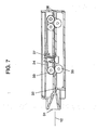
wiring terminal 8, being disposed ingroove 26 securely, can be easily inserted into printedwiring board 20. - Next, an operation of bill validator is described. Fig. 7 shows a cross-sectional view of a bill validator having a magnetic-sensor-
assembly 27, described in Figs 4, 5, and 6 with reference to the first exemplary embodiment of the invention. - In Fig. 7, inlet opening 31 of
bill 12 is coupled to bill pass-way 32. Magnetic-sensor-assembly 27 disclosed in the first exemplary embodiment is mounted on a wall of pass-way 32. In addition to this, a transportationsystem comprising pulley 33 andbelt 34 is provided with bill pass-way 32.Roller 35 functions to pressbill 12.Outlet 36 ofbill 12 is provided at an end of bill pass-way 32. - Fig. 8 shows a block diagram of the bill validator using magnetic-sensor-
assembly 27 disclosed in the first exemplary embodiment.
In magnetic-sensor-assembly 27 shown in Fig. 8, two artificial-lattice MR element board 2, and electrically connected to power in one end and to ground in another end. Two artificial-lattice MR elements - Next,
pattern 6A, coupling section of artificial-lattice MR element amplifier 41. Output signals fromamplifier 41 is fed into sample/hold circuit 42, then output signals fromamplifier 41 is tapped off toevaluation circuit 45 inmicroprocessor 44 through analog/digital converter (A/D converter). - Additionally, sampling/
signal circuit 46 is connected to sample/hold circuit 42 and A/D converter 43. Bill validation data and the like are stored inmemory 47. - Next, an operation of aforementioned bill validator is described. First, voltage of
coupling section 6A increases due to reduction in electrical resistance of artificial-lattice MR element 1A, when artificial-lattice MR element 1A senses magnetic field of magnetic features applied onbill 12. Next, both of artificial-lattice MR element bill 12. Consequently, voltage ofcoupling section 6A decreases to half value ofvoltage supply 40 due to reduction in electrical resistance of both of artificial-lattice MR element - Next, only artificial-
lattice MR element 1B senses magnetic field of magnetic features applied onbill 12, whenbill 12 leaves away from artificial-lattice MR element 1A. Then, voltage ofcoupling section 6A decreases due to increase in electrical resistance of artificial-lattice MR element 1A and decrease in electrical resistance of artificial-lattice MR element 1B. - Voltage of
coupling section 6A returns back to initial value (half value of voltage supply 40) due to increase in electrical resistance of both of artificial-lattice MR element bill 12 leave away from artificial-lattice MR element 1B. - In the above mentioned operation,
magnetic sensor assembly 27 taps off characteristic signals as shown in Fig. 9. The signal is fed to sample/hold circuit 42 after amplified inamplifier 41. - Sample/
hold circuit 42 has a purpose to prevent errors in reading in A/D converter 43, as tapped off signal frommagnetic sensor assembly 27 has narrow width pulsed wave-shape. Hence, A/D converter 42 can read signals correctly after peak value of the signal is held for a certain period of time in sample/hold circuit 42 as shown in Fig. 10. Sample /hold circuit 42 holds the maximum level of signal. After reading in A/D converter circuit for a certain period of time, the circuit is reset by a signal from samplingcircuit 46. The certain period of time for holding the maximum peak value is necessarily longer than sampling interval of A/D converter circuit 43. In Figs. 9 and 10, horizontal axis denotes time (in ms) and vertical axis denotes level (in mV). Subsequently, A/D converter circuit 43 converts magnetic signal of bill into digital signal, andvalidation circuit 45 determines validity and denomination ofbill 12. - As described above, in this first exemplary embodiment, the bill validator performs with high accuracy in detection due to artificial-
lattice MR element 1 used in magnetic-sensor-assembly 27 of the bill validator. - The bill validator performs with high accuracy due to artificial-
lattice MR element 1 formed in magnetic-sensor-assembly 27 of the bill validator. Hence, the bill validator can detectbill 12 if inserted in reversed position. - Additionally,
validation circuit 45 validatesbill 12 by a maximum signal value detected, for example, in adjacent to prescribed measurement area. In this case, a bill validator comprised of magnetic-sensor-assembly 27 having highly sensitive artificial-lattice MR element 1 can detect magnetic features ofbill 12 with high accuracy. - Moreover, bill validation is also possible by a maximum to minimum ratio of signals detected in adjacent to a prescribed area. The validation can be free from environmental condition, since judgment depends upon the maximum to minimum ratio, a relative comparison.
- Furthermore, bill validation is also possible by detecting an order of occurrence of maximum and minimum output signals from magnetic-sensor-
assembly 27. In this case, utilizing relationship between time and signal level, a bill validator can detect with high accuracy. - Moreover, bill validation is also possible by detecting a difference between a peak signal level from
magnetic sensor assembly 27 at a certain area onbill 12, and a signal level at a prescribed area onbill 12. In this case, data of area onbill 12 where peak signal level is shown and the peak signal level can be well utilized for bill validation. - When above mentioned methods are adopted together as appropriate. validation accuracy can be improved more.
- In this second exemplary embodiment, a magnetic sensor comprised of four artificial-lattice MR (magnetic resistor) elements is described. The description is mainly on differences between the first and the second exemplary embodiments of this invention. As to corresponding parts to the first exemplary embodiment, description is simplified by coding 100 order referring marks to corresponding parts of the first exemplary embodiment.
- Fig. 11 is a plan view of a magnetic sensor used in the second exemplary embodiment of this invention.
Etching the above-mentioned multi-layer artificial-lattice MR element, described in Fig. 2 of the first exemplary embodiment, forms a circuitry shown in Fig. 11. Namely, coupling four artificial-lattice MR element conductive patterns
through-holes ceramic board 102 so that a bridge circuit is formed. - As clear from above, a simple circuit configuration, like shown in Fig. 11, can detect change of magnetic field with high sensitivity, when four artificial-lattice MR elements are arranged so that magnetic media passes in front of each artificial-lattice MR elements, sequentially in the order.
- Referring to Fig. 1, artificial-
lattice MR element 1 represents 101A, 101B, 101C and 101D. Similarly, pattern 6 represents 106A, 106B, 106C and 106D. Through-hole 7 represents 107A, 107B, 107C and 107D.Wiring terminal 8 represents 108A, 108B, 108C and 108D. - Fig. 12 shows a block diagram of a bill validator equipped with
magnetic sensor assembly 127 described in the second exemplary embodiment of the present invention.Magnetic sensor assembly 127 is the same asmagnetic sensor assembly 27 described in the first exemplary embodiment of the invention, except that four, not two, artificial-lattice MR elements, 101A, 101B, 101C and 101D are provided. - In magnetic-sensor-
assembly 127, four artificial-lattice MR elements, 101A, 101B, 101C and 101D, each having approximately similar properties, are coupled in series onboard 102. Among four resulting coupling sections,pattern pattern differential amplifier 141. - Four artificial-
lattice MR elements differential amplifier 141 is similar to circuitry shown in Fig. 8 of the first exemplary embodiment of this invention. - Next, operation of bill validator configurated as above is described, but differences between the first and the second exemplary embodiments of this invention only. Namely, artificial-lattice MR elements detect magnetic field of magnetic features printed on
bill 12, sequentially in the order of 101A, 101C, 101B and 101D. Similar to Fig. 8 of the first exemplary embodiment of this invention, voltage ofcoupling section bill 12 leave away from artificial-lattice MR element 101D. Since a bill validator shown in Fig. 12 functions to detect voltage variation betweencoupling sections assembly 127 is little influenced by environmental magnetic noise. Additionally, the same descriptions as the first exemplary embodiment are simplified here. - As mentioned above, magnetic sensor disclosed in this invention comprises an artificial-lattice MR element formed on a face of a board to detect magnetic field features of a media passing close to the face of the board. The artificial-lattice MR element formed on the board and wiring terminals coupled to the artificial-lattice MR element are integrated in a housing with resin. Moreover, a magnet is mounted at the back of the board in the housing to provide a plane of artificial MR element with an auxiliary magnetic field perpendicularly. The artificial-lattice MR element provided in the magnetic sensor performs with high sensitivity in bill validation. Hence, the magnetic sensor can detect magnetic ink of a bill even on the back or even if being inserted in any direction.
- The magnet, adopted to provide a plane of artificial-lattice MR element with an auxiliary magnetic field perpendicularly, provides the magnetic sensor with high accuracy in validation when adopted in a bill validator.
Claims (21)
- A magnetic sensor comprising:(a) an artificial-lattice magnetic resistor (MR) element formed on a face of a board to detect a magnetic media passing close to a face of the board;(b) the artificial-lattice MR element and wiring terminals coupled to the artificial-lattice MR element being integrated in a housing with
resin;
and(c) a magnet, mounted at the back of the board in the housing to provide a plane of artificial-lattice MR element with an auxiliary magnetic field perpendicularly. - The magnetic sensor of claim 1, wherein the artificial-lattice MR element has a multi-layer structure comprising not less than each ten layers of Cu layer, 10 to 30Å thick, and Ni-Fe-Co layer, 20 to 40Å thick, sandwiched alternately.
- The magnetic sensor of claim 2, wherein a coupled section and both ends of series-of-MR, comprising two artificial-lattice MR element coupled in series and arranged in parallel, are coupled to the wiring terminals.
- The magnet sensor of claim 1, wherein the magnet provides with magnetic flux density of 15 to 30 mT at surface of the artificial-lattice MR element.
- The magnet sensor of claim 1, wherein the magnet is formed from a material composed of magnetic ferrite powder, mixed and dispersed in at least one of resin or rubber base material.
- The magnet sensor of claim 1, further comprising a housing with a hollow for the magnet to be embedded.
- The magnet sensor of claim 1, further comprising:a case composed of resin to house the magnetic sensor of claim 3, whereinthe case comprises an opening against artificial-lattice MR element and grooves to dispose the wiring terminals.
- The magnet sensor of claim 7, further comprising:a resin cap to cover opening of resin case having the artificial-lattice MR element.
- The magnet sensor of claim 8, wherein the cap is fitted and secured to case by elastic deformation property.
- The magnet sensor of claim 8, further comprising:a hook formed on opposite side of opening of the case to secure to outside printed wiring board in an elastic deformation property.
- The magnet sensor of claim 8, further comprising:a boss integrated on the case to secure to outside printed wiring board using a screw.
- A bill validator comprising:(d) a bill inlet opening;(e) a bill pass-way coupled to the bill inlet opening;(f) the magnetic sensor, described in claim 8, mounted on a wall of the bill pass-way;(g) an amplifier electrically connected to the magnet sensor;(h) an analog/digital converter (A/D converter) electrically connected to output of the amplifier;
and(i) an evaluation circuit electrically connected to output of the A/D converter. - The bill validator of claim 12, further comprising:a sample/hold circuit, having a time-constant longer than sampling cycle of the A/D converter, between the amplifier and the A/D converter.
- The bill validator of claim 13, further comprising:a printed wiring board having the magnetic sensor with an air space just below the magnetic sensor;
anda circuit component electrically connected to the magnetic sensor disposed in the air space. - The bill validator of claim 13, wherein validation circuit validates the bill by the maximum signal value detected in adjacent to prescribed measurement area of the bill.
- The bill validator of claim 13, wherein validation circuit validates the bill by the maximum to minimum ratio of signals detected in adjacent to prescribed measurement area of the bill.
- The bill validator of claim 13, wherein validation circuit validates the bill by detecting an order of occurrence of maximum and minimum output signal from magnetic sensor.
- The bill validator of claim 13, wherein validation circuit validates the bill by detecting with a position on the bill which outputs a peak signal level from magnetic-sensor-assembly and a difference between a peak signal level from magnetic-sensor-assembly at an area on the bill and a signal level at a prescribed area on the bill.
- The magnetic sensor of claim 2, wherein four coupled sections of series-of-MR, comprising four artificial-lattice MR element coupled in series in ring-form and arranged each in parallel, are electrically connected to the respective wiring terminals.
- A magnetic-sensor-assembly comprising:the magnetic sensor described in claim 19;a resin case having grooves to dispose the wiring terminals;
anda resin cap to cover opening of the resin case facing the artificial-lattice MR element. - A bill validator comprising:a bill inlet opening;a bill pass-way coupled to the bill inlet opening;the magnetic-sensor-assembly, described in claim 20, disclosed mounted on a wall of the bill pass-way;a differential amplifier electrically connected to the magnetic-sensor-assembly;an A/D converter electrically connected to output of the differentialamplifier;
andan evaluation circuit electrically connected to output of the A/D converter.
Applications Claiming Priority (4)
| Application Number | Priority Date | Filing Date | Title |
|---|---|---|---|
| JP2001146215 | 2001-05-16 | ||
| JP2001146215 | 2001-05-16 | ||
| JP2002066472 | 2002-03-12 | ||
| JP2002066472A JP3603872B2 (en) | 2001-05-16 | 2002-03-12 | Magnetic sensor and banknote recognition device using it |
Publications (3)
| Publication Number | Publication Date |
|---|---|
| EP1258841A2 true EP1258841A2 (en) | 2002-11-20 |
| EP1258841A3 EP1258841A3 (en) | 2004-01-07 |
| EP1258841B1 EP1258841B1 (en) | 2008-04-16 |
Family
ID=26615173
Family Applications (1)
| Application Number | Title | Priority Date | Filing Date |
|---|---|---|---|
| EP02010180A Expired - Lifetime EP1258841B1 (en) | 2001-05-16 | 2002-05-14 | Magnetic sensor and bill validator using the same |
Country Status (5)
| Country | Link |
|---|---|
| EP (1) | EP1258841B1 (en) |
| JP (1) | JP3603872B2 (en) |
| CN (1) | CN1178175C (en) |
| DE (1) | DE60226092T2 (en) |
| ES (1) | ES2304406T3 (en) |
Cited By (1)
| Publication number | Priority date | Publication date | Assignee | Title |
|---|---|---|---|---|
| US10663320B2 (en) | 2016-11-25 | 2020-05-26 | Mitsubishi Electric Corporation | Magnetic sensor device |
Families Citing this family (7)
| Publication number | Priority date | Publication date | Assignee | Title |
|---|---|---|---|---|
| JP4507585B2 (en) * | 2003-12-16 | 2010-07-21 | 日本電産サンキョー株式会社 | Drive circuit for paper sheet identification sensor and paper sheet identification device |
| JP4771738B2 (en) * | 2005-05-02 | 2011-09-14 | 日本電産サンキョー株式会社 | Paper sheet identification device and magnetic sensor for paper sheet identification |
| CN104063938B (en) * | 2010-02-05 | 2016-09-21 | 日本电产三协株式会社 | Magnetic pattern detecting apparatus |
| CN102722932A (en) * | 2012-06-19 | 2012-10-10 | 兰州大学 | Magnetic head of currency detector |
| CN104215920B (en) * | 2013-06-03 | 2019-02-15 | 北京嘉岳同乐极电子有限公司 | A kind of chip magnetic measurement sensor |
| JP2017122598A (en) * | 2016-01-05 | 2017-07-13 | グローリー株式会社 | Magneto detection device, paper sheet identification device and magneto detection method |
| JP7143690B2 (en) * | 2018-09-03 | 2022-09-29 | 株式会社島津製作所 | Magnetic material inspection system, magnetic material inspection apparatus, and magnetic material inspection method |
Citations (6)
| Publication number | Priority date | Publication date | Assignee | Title |
|---|---|---|---|---|
| US3870629A (en) * | 1973-10-11 | 1975-03-11 | Umc Ind | Paper currency validator |
| US4973851A (en) * | 1989-04-07 | 1990-11-27 | Rowe International, Inc. | Currency validator |
| EP0863406A2 (en) * | 1997-03-07 | 1998-09-09 | Alps Electric Co., Ltd. | Magnetoresistive sensor |
| US5929636A (en) * | 1996-05-02 | 1999-07-27 | Integrated Magnetoelectronics | All-metal giant magnetoresistive solid-state component |
| US6069476A (en) * | 1996-08-08 | 2000-05-30 | Commissariat A L'energie Atomique | Magnetic field sensor having a magnetoresistance bridge with a pair of magnetoresistive elements featuring a plateau effect in their resistance-magnetic field response |
| WO2000079298A2 (en) * | 1999-06-18 | 2000-12-28 | Koninklijke Philips Electronics N.V. | Magnetic systems with irreversible characteristics and a method of manufacturing and repairing and operating such systems |
Family Cites Families (13)
| Publication number | Priority date | Publication date | Assignee | Title |
|---|---|---|---|---|
| JPS585869U (en) * | 1981-07-03 | 1983-01-14 | 株式会社ブリヂストン | pillow |
| JPS57177182U (en) * | 1982-01-07 | 1982-11-09 | ||
| JPS62242291A (en) * | 1986-04-14 | 1987-10-22 | 富士電機株式会社 | Identification of sheet paper |
| JPH0396867A (en) * | 1989-09-08 | 1991-04-22 | Fuji Electric Co Ltd | Current display circuit for non-linear load |
| JP2859720B2 (en) * | 1990-08-03 | 1999-02-24 | 富士通株式会社 | Semiconductor integrated circuit tester |
| JPH05113472A (en) * | 1991-10-22 | 1993-05-07 | Fujitsu Ltd | Magnetic sensor |
| JP2909683B2 (en) * | 1992-03-13 | 1999-06-23 | アンリツ株式会社 | Coin diameter discriminator |
| JP3283930B2 (en) * | 1992-12-11 | 2002-05-20 | グローリー工業株式会社 | Magnetic material detection method |
| JP3276264B2 (en) * | 1995-05-26 | 2002-04-22 | アルプス電気株式会社 | Magnetoresistive multilayer film and method of manufacturing the same |
| JP3941148B2 (en) * | 1997-03-10 | 2007-07-04 | 松下電器産業株式会社 | Manufacturing method of magnetic sensor |
| JPH11265818A (en) * | 1998-03-16 | 1999-09-28 | Bridgestone Corp | Composition for resin magnet and magnet roller using the same |
| JP2000180207A (en) * | 1998-12-16 | 2000-06-30 | Yazaki Corp | Magnetism sensor |
| JP2000304838A (en) * | 1999-04-20 | 2000-11-02 | Sankyo Seiki Mfg Co Ltd | Magnetic sensor |
-
2002
- 2002-03-12 JP JP2002066472A patent/JP3603872B2/en not_active Expired - Lifetime
- 2002-05-14 DE DE60226092T patent/DE60226092T2/en not_active Expired - Lifetime
- 2002-05-14 ES ES02010180T patent/ES2304406T3/en not_active Expired - Lifetime
- 2002-05-14 EP EP02010180A patent/EP1258841B1/en not_active Expired - Lifetime
- 2002-05-16 CN CNB021197989A patent/CN1178175C/en not_active Expired - Fee Related
Patent Citations (6)
| Publication number | Priority date | Publication date | Assignee | Title |
|---|---|---|---|---|
| US3870629A (en) * | 1973-10-11 | 1975-03-11 | Umc Ind | Paper currency validator |
| US4973851A (en) * | 1989-04-07 | 1990-11-27 | Rowe International, Inc. | Currency validator |
| US5929636A (en) * | 1996-05-02 | 1999-07-27 | Integrated Magnetoelectronics | All-metal giant magnetoresistive solid-state component |
| US6069476A (en) * | 1996-08-08 | 2000-05-30 | Commissariat A L'energie Atomique | Magnetic field sensor having a magnetoresistance bridge with a pair of magnetoresistive elements featuring a plateau effect in their resistance-magnetic field response |
| EP0863406A2 (en) * | 1997-03-07 | 1998-09-09 | Alps Electric Co., Ltd. | Magnetoresistive sensor |
| WO2000079298A2 (en) * | 1999-06-18 | 2000-12-28 | Koninklijke Philips Electronics N.V. | Magnetic systems with irreversible characteristics and a method of manufacturing and repairing and operating such systems |
Cited By (1)
| Publication number | Priority date | Publication date | Assignee | Title |
|---|---|---|---|---|
| US10663320B2 (en) | 2016-11-25 | 2020-05-26 | Mitsubishi Electric Corporation | Magnetic sensor device |
Also Published As
| Publication number | Publication date |
|---|---|
| EP1258841B1 (en) | 2008-04-16 |
| CN1385816A (en) | 2002-12-18 |
| DE60226092D1 (en) | 2008-05-29 |
| EP1258841A3 (en) | 2004-01-07 |
| DE60226092T2 (en) | 2009-07-02 |
| JP3603872B2 (en) | 2004-12-22 |
| JP2003035701A (en) | 2003-02-07 |
| ES2304406T3 (en) | 2008-10-16 |
| CN1178175C (en) | 2004-12-01 |
Similar Documents
| Publication | Publication Date | Title |
|---|---|---|
| US8581578B2 (en) | Magnetic pattern detection device | |
| JP6276283B2 (en) | Magnetic currency verification head | |
| EP0232174B1 (en) | Tokens and apparatus for handling tokens | |
| EP0670073B1 (en) | A capacitive verification device for a security thread embedded within currency paper | |
| US20090152356A1 (en) | Non-contact magnetic pattern recognition sensor | |
| US20040012875A1 (en) | Magnetic read head having decode circuitry | |
| CA1228743A (en) | Cylinder lock-key combination with an electronic evaluation circuit for establishing proper actuation of the cylinder, and a lock cylinder and key for such a combination | |
| US5180903A (en) | Magnetic detecting unit having aligned sensors | |
| JP2581421Y2 (en) | Magnetic sensor | |
| EP1258841B1 (en) | Magnetic sensor and bill validator using the same | |
| KR880000755B1 (en) | Verifying system | |
| US4975675A (en) | Device comprising at least one magneto-resistor contained in a housing | |
| JP6359858B2 (en) | Magnetic field detection device and magnetic identification device | |
| KR20150125919A (en) | Magnetic head for detecting soft and hard magnetic characteristic signals | |
| CN101777206B (en) | Magnetic sensor and device for identifying sheet | |
| CN101167106B (en) | Magnetic sensor and paper sheet identification device | |
| WO2014005431A1 (en) | Chip-type magnetic sensor | |
| US5764054A (en) | Contiguously matched magnetic sensor array and magnetic media for authentication of documents and products | |
| US11614500B2 (en) | Integrated magnetometer and method of detecting a magnetic field | |
| CN113302693A (en) | Magnetic identification sensor | |
| EP0777213A1 (en) | Flux-guided paired magnetoresistive head | |
| JPH0285982A (en) | Method and device for recognizing magnetic pattern | |
| JPH10155969A (en) | Pachinko ball detecting switch | |
| KR20050019925A (en) | Magnetic sensing device | |
| JPH10275309A (en) | Magneto-resistance effect type head |
Legal Events
| Date | Code | Title | Description |
|---|---|---|---|
| PUAI | Public reference made under article 153(3) epc to a published international application that has entered the european phase |
Free format text: ORIGINAL CODE: 0009012 |
|
| AK | Designated contracting states |
Kind code of ref document: A2 Designated state(s): AT BE CH CY DE DK ES FI FR GB GR IE IT LI LU MC NL PT SE TR |
|
| AX | Request for extension of the european patent |
Free format text: AL;LT;LV;MK;RO;SI |
|
| PUAL | Search report despatched |
Free format text: ORIGINAL CODE: 0009013 |
|
| RIC1 | Information provided on ipc code assigned before grant |
Ipc: 7G 01R 33/09 B Ipc: 7G 07D 7/04 A |
|
| AK | Designated contracting states |
Kind code of ref document: A3 Designated state(s): AT BE CH CY DE DK ES FI FR GB GR IE IT LI LU MC NL PT SE TR |
|
| AX | Request for extension of the european patent |
Extension state: AL LT LV MK RO SI |
|
| 17P | Request for examination filed |
Effective date: 20040315 |
|
| AKX | Designation fees paid |
Designated state(s): DE ES GB IT |
|
| 17Q | First examination report despatched |
Effective date: 20041105 |
|
| GRAP | Despatch of communication of intention to grant a patent |
Free format text: ORIGINAL CODE: EPIDOSNIGR1 |
|
| GRAS | Grant fee paid |
Free format text: ORIGINAL CODE: EPIDOSNIGR3 |
|
| GRAA | (expected) grant |
Free format text: ORIGINAL CODE: 0009210 |
|
| AK | Designated contracting states |
Kind code of ref document: B1 Designated state(s): DE ES GB IT |
|
| REF | Corresponds to: |
Ref document number: 60226092 Country of ref document: DE Date of ref document: 20080529 Kind code of ref document: P |
|
| REG | Reference to a national code |
Ref country code: ES Ref legal event code: FG2A Ref document number: 2304406 Country of ref document: ES Kind code of ref document: T3 |
|
| RAP2 | Party data changed (patent owner data changed or rights of a patent transferred) |
Owner name: PANASONIC CORPORATION |
|
| PLBE | No opposition filed within time limit |
Free format text: ORIGINAL CODE: 0009261 |
|
| STAA | Information on the status of an ep patent application or granted ep patent |
Free format text: STATUS: NO OPPOSITION FILED WITHIN TIME LIMIT |
|
| 26N | No opposition filed |
Effective date: 20090119 |
|
| PG25 | Lapsed in a contracting state [announced via postgrant information from national office to epo] |
Ref country code: IT Free format text: LAPSE BECAUSE OF FAILURE TO SUBMIT A TRANSLATION OF THE DESCRIPTION OR TO PAY THE FEE WITHIN THE PRESCRIBED TIME-LIMIT Effective date: 20080416 |
|
| PGFP | Annual fee paid to national office [announced via postgrant information from national office to epo] |
Ref country code: ES Payment date: 20120518 Year of fee payment: 11 |
|
| PGFP | Annual fee paid to national office [announced via postgrant information from national office to epo] |
Ref country code: DE Payment date: 20130515 Year of fee payment: 12 Ref country code: GB Payment date: 20130508 Year of fee payment: 12 |
|
| REG | Reference to a national code |
Ref country code: DE Ref legal event code: R119 Ref document number: 60226092 Country of ref document: DE |
|
| GBPC | Gb: european patent ceased through non-payment of renewal fee |
Effective date: 20140514 |
|
| REG | Reference to a national code |
Ref country code: DE Ref legal event code: R119 Ref document number: 60226092 Country of ref document: DE Effective date: 20141202 |
|
| PG25 | Lapsed in a contracting state [announced via postgrant information from national office to epo] |
Ref country code: DE Free format text: LAPSE BECAUSE OF NON-PAYMENT OF DUE FEES Effective date: 20141202 |
|
| PG25 | Lapsed in a contracting state [announced via postgrant information from national office to epo] |
Ref country code: GB Free format text: LAPSE BECAUSE OF NON-PAYMENT OF DUE FEES Effective date: 20140514 |
|
| REG | Reference to a national code |
Ref country code: ES Ref legal event code: FD2A Effective date: 20150626 |
|
| PG25 | Lapsed in a contracting state [announced via postgrant information from national office to epo] |
Ref country code: ES Free format text: LAPSE BECAUSE OF NON-PAYMENT OF DUE FEES Effective date: 20140515 |