EP1258830A2 - Verfahren zum Abgleich eines Antennenschwingkreises eines passiven Transponders - Google Patents
Verfahren zum Abgleich eines Antennenschwingkreises eines passiven Transponders Download PDFInfo
- Publication number
- EP1258830A2 EP1258830A2 EP02010096A EP02010096A EP1258830A2 EP 1258830 A2 EP1258830 A2 EP 1258830A2 EP 02010096 A EP02010096 A EP 02010096A EP 02010096 A EP02010096 A EP 02010096A EP 1258830 A2 EP1258830 A2 EP 1258830A2
- Authority
- EP
- European Patent Office
- Prior art keywords
- zone
- antenna
- capacitance
- integrated circuit
- contact surface
- Prior art date
- Legal status (The legal status is an assumption and is not a legal conclusion. Google has not performed a legal analysis and makes no representation as to the accuracy of the status listed.)
- Granted
Links
Images

Classifications
-
- G—PHYSICS
- G06—COMPUTING OR CALCULATING; COUNTING
- G06K—GRAPHICAL DATA READING; PRESENTATION OF DATA; RECORD CARRIERS; HANDLING RECORD CARRIERS
- G06K19/00—Record carriers for use with machines and with at least a part designed to carry digital markings
- G06K19/06—Record carriers for use with machines and with at least a part designed to carry digital markings characterised by the kind of the digital marking, e.g. shape, nature, code
- G06K19/067—Record carriers with conductive marks, printed circuits or semiconductor circuit elements, e.g. credit or identity cards also with resonating or responding marks without active components
- G06K19/07—Record carriers with conductive marks, printed circuits or semiconductor circuit elements, e.g. credit or identity cards also with resonating or responding marks without active components with integrated circuit chips
- G06K19/0723—Record carriers with conductive marks, printed circuits or semiconductor circuit elements, e.g. credit or identity cards also with resonating or responding marks without active components with integrated circuit chips the record carrier comprising an arrangement for non-contact communication, e.g. wireless communication circuits on transponder cards, non-contact smart cards or RFIDs
- G06K19/0726—Record carriers with conductive marks, printed circuits or semiconductor circuit elements, e.g. credit or identity cards also with resonating or responding marks without active components with integrated circuit chips the record carrier comprising an arrangement for non-contact communication, e.g. wireless communication circuits on transponder cards, non-contact smart cards or RFIDs the arrangement including a circuit for tuning the resonance frequency of an antenna on the record carrier
-
- G—PHYSICS
- G06—COMPUTING OR CALCULATING; COUNTING
- G06K—GRAPHICAL DATA READING; PRESENTATION OF DATA; RECORD CARRIERS; HANDLING RECORD CARRIERS
- G06K19/00—Record carriers for use with machines and with at least a part designed to carry digital markings
- G06K19/06—Record carriers for use with machines and with at least a part designed to carry digital markings characterised by the kind of the digital marking, e.g. shape, nature, code
- G06K19/067—Record carriers with conductive marks, printed circuits or semiconductor circuit elements, e.g. credit or identity cards also with resonating or responding marks without active components
- G06K19/07—Record carriers with conductive marks, printed circuits or semiconductor circuit elements, e.g. credit or identity cards also with resonating or responding marks without active components with integrated circuit chips
- G06K19/0723—Record carriers with conductive marks, printed circuits or semiconductor circuit elements, e.g. credit or identity cards also with resonating or responding marks without active components with integrated circuit chips the record carrier comprising an arrangement for non-contact communication, e.g. wireless communication circuits on transponder cards, non-contact smart cards or RFIDs
-
- G—PHYSICS
- G06—COMPUTING OR CALCULATING; COUNTING
- G06K—GRAPHICAL DATA READING; PRESENTATION OF DATA; RECORD CARRIERS; HANDLING RECORD CARRIERS
- G06K19/00—Record carriers for use with machines and with at least a part designed to carry digital markings
- G06K19/06—Record carriers for use with machines and with at least a part designed to carry digital markings characterised by the kind of the digital marking, e.g. shape, nature, code
- G06K19/067—Record carriers with conductive marks, printed circuits or semiconductor circuit elements, e.g. credit or identity cards also with resonating or responding marks without active components
- G06K19/07—Record carriers with conductive marks, printed circuits or semiconductor circuit elements, e.g. credit or identity cards also with resonating or responding marks without active components with integrated circuit chips
- G06K19/077—Constructional details, e.g. mounting of circuits in the carrier
- G06K19/07749—Constructional details, e.g. mounting of circuits in the carrier the record carrier being capable of non-contact communication, e.g. constructional details of the antenna of a non-contact smart card
Definitions
- the present invention relates to a method for adjusting an antenna resonant circuit a passive transponder, according to the preamble of claim 1.
- Passive transponders are used in the area of contactless communication for identification (RFID) used.
- RFID identification
- the carrier wave emitted by the base station is replaced by the Transponder modulated.
- passive transponders do not have their own energy supply, must the energy for the integrated circuit of the passive transponder, by absorption modulation be removed from the carrier wave.
- passive 125 kHz systems this is achieved in the electromagnetic near field by inductive coupling.
- the energy range achieved in this way is in the range of a few cm to approximately 0.5 m and depends on the respective national RF regulations.
- With the increasing Security requirements for identification are becoming ever higher data transmission rates needed to keep identification times short. This is only with high carrier frequencies in the UHF (868 MHz) or microwave range (2.45 GHz). With these Frequently dipole antennas are used. Development goal in this The area is, with passive systems long ranges with reasonable transmission powers the base station.
- the length of the dipole antenna is to be adapted to the wavelength of the transmitter.
- the wave resistance specified by the design of the antenna is achieved, that a complete absorption of the received electromagnetic wave takes place.
- the transponder antenna is at a greater distance from the transmitter resulting antenna voltage too low to result from a simple rectification generate a supply voltage for the transponder. Due to the RF regulations In the European countries, the ranges of existing UHF transponders are under a meter.
- the object of the present invention is to provide a method for adjusting an antenna resonant circuit a passive transponder, by means of which the range of a passive transponders for a high-frequency electromagnetic carrier field is increased.
- the second task is to specify a semiconductor arrangement for implementing the method.
- the first-mentioned object is achieved according to the invention by a method of the aforementioned Art solved with the features of claim 1.
- the second task is solved by the features of claim 6.
- Favorable design forms are Subject of subclaims.
- the essence of the invention is the range of a passive transponder to increase by capacitively absorbing that from a high frequency electrical field
- Operating energy by means of a serial resonant circuit exclusively an input part of the transponder to generate a supply voltage for the integrated Circuit is provided.
- a semiconductor body with an integrated circuit with a signal part with reference potential connection and one antenna arrangement arranged on a carrier has, and the antenna arrangement via a connected to the semiconductor body Contact area is connected to the integrated circuit, and in which the antenna forms a serial resonant circuit with the input capacitance of the integrated circuit, the parasitic capacitive and resistive to increase the quality of the antenna resonant circuit Shares that have a current path between the contact area (BP) and the reference potential form, reduced.
- BP contact area
- the advantage of the new method is that the very small antenna voltage high voltage values generated by means of the serial resonant circuit are not produced by the Contact surface connected parasitic capacitive and resistive components are absorbed.
- the power absorbed by the antenna is the input part of the integrated Circuit for generating the supply voltage available.
- the serial The resonant circuit has only a very small inductance, with the reduction of the capacitive Share (imaginary part) of the contact surface reaches that the quality of the signal part increases leaves. Due to the improved efficiency of the receiving part of the transponder, the range of passive RFID systems is increased considerably.
- the current path between the contact area and the reference potential at at least one point by means of a series connection and parallel connection of capacitive and resistive components, in a first Split current path and a second current path by a first high capacity Goodness and a parallel connection, of a small capacitance, the capacitance value of which is preferred is in the range of a few fF (10e-18 Farad), with low quality and a small one Capacitance, the capacitance value of which is preferably in the range of a few fF, with high quality, is connected in series.
- the small capacities are used Diodes generated because the PN junctions necessary for the production of diodes are in the Simply let the manufacturing process of the integrated circuit be realized. Furthermore, Create spatially limited PN junctions that have a low capacitance. Furthermore, it is advantageous to generate the first capacitance, which requires a high quality, by placing a conductive in an insulation layer below the contact surface Layer is drawn in.
- the HF equivalent circuit diagram shown in FIG. 1 describes the structure of a receiving section of a passive transponder TR for energy absorption by absorption from one high-frequency electromagnetic carrier field of a base station (not shown).
- the Transponder TR consists of an antenna AN and an integrated circuit IS, both of which are arranged in a common housing (not shown).
- the antenna AN with the integrated circuit IS by means of a contact surface BP and a bonding wire connected, the contact surface BP within the integrated circuit IS with a signal part ST is connected.
- the antenna AN is in series with a parallel connection the contact area BP and the signal part ST.
- the task of the signal part ST for example contains a voltage doubler circuit, it is by means of the antenna AN absorbed energy to generate a supply voltage for the integrated circuit IS.
- the antenna AN consists in the equivalent circuit of an alternating voltage generator GA, which with the Reference potential is connected and a series resistor RA. Furthermore, the series resistance RA connected to a coil L1, which is in series with the parallel connection of the contact surface BP and the signal part ST is connected.
- the contact surface BP consists of a series connection of a capacitor CP and one connected to the reference potential Resistance RP.
- the signal part ST can be made from a series connection of a capacitor CS and a load resistor RS connected to the reference potential.
- the AC voltage generator GA describes that of the antenna AN from the carrier field of the base station (not shown) absorbed energy, which in the form of an AC voltage, the series resonant circuit excited, which consists of the resistor RA, the coil L1, and the capacitors CP and CS and the resistors RP and RS is formed.
- the one with excitation in the antenna AN occurring loss is described by the resistance RA, the phase shift between current and voltage in the antenna through the coil L1.
- the loss as the real part and the phase shift as Imaginary part shown.
- the contact surface BP with an imaginary part is shown by the capacitor CP, and a real part, represented by the resistor RP.
- the signal part ST also has an imaginary part, represented by the capacitor CS, and a real part, represented by the resistor RS.
- the resonance frequency of the series resonant circuit is either at the carrier frequency 868 MHz or 2.45 GHz matched.
- the total capacitance of the two capacitors CP and CS, and the inductance of the coil L1 meet the resonance condition.
- the series resonant circuit becomes the excitation voltage of the AC voltage generator which is in the range of a few ⁇ V GA increased in proportion to the quality of the series resonant circuit.
- the damping must the sum of the Real parts are small and the ratio of the imaginary parts of inductance and capacitance is large, around all the energy absorbed from the carrier field the signal part at a high To provide voltage level for generating a supply voltage.
- the inductance value of the coil L1 is small, the capacitance values of the capacitors CP and CS have very small values in the range around the series resonant circuit on the resonance frequency to match the carrier frequency, i.e. the one connected to the contact surface BP Capacity CP (imaginary part) must be reduced.
- the one with the Contact area BP connected real part must be very small to ensure high quality in the series resonant circuit to achieve and the absorbed energy the signal part ST, represented by the Resistor RS, for generating the supply voltage for the integrated circuit IS To make available.
- the cross section shown in FIG. 2a through a contact area within an integrated semiconductor arrangement shows the prior art to date.
- the designation DA designates a mirror axis, ie the illustration shown is symmetrical to the axis DA.
- the function of the contact area is to provide an area for receiving a bond in order to connect the antenna AN to the integrated circuit IS.
- the structure of the cross-sectional image is explained below in conjunction with a simplified AC voltage analysis.
- an insulation layer ISO is formed which isolates the contact area ALB1 from an underlying low-doped zone D1 of a first conductivity type.
- a lightly doped zone D2 of the second conductivity type adjoining the zone D1 which is generally referred to as substrate doping, characterizes the reference potential and is connected to a contact ALK by means of a highly doped zone D2P, of the second conductivity type.
- a large minimum distance a1 must be maintained between the contact area ALB1 and the contact ALK, which is in the range of a few 10 microns, and the length of the zone D2 between the zone D1 and zone D2P.
- the layer sequence of the contact area and the zone D1 corresponds to a capacitor with a capacitance coating CP, the lightly doped zone D1 of the opposite conductivity type to the substrate doping having the effect that the capacitive contribution CP of the contact areas does not become very large.
- a resistor RP In series with the capacitor CP is a resistor RP, which has a high value due to the large length of the zone D2 in conjunction with the low doping.
- the contact area ALB1 and the zone D1 form a capacitor with the capacitance C1.
- a diode DD1D2 which is formed by the interface of zones D1 / D2 will, and a resistor RS1, which is the length of the zone D2 between the diode DD1D2 and the contact ALK results.
- the diode DD1D2 is used as a parallel circuit from a resistor XRC2 and a capacitor C2 and one in Series switched resistor RSC2 shown.
- the total capacity CP is determined the series resistance RP results from the sum of the capacitance values C1 and C2 the sum of the resistances RSC2 and RS1.
- the capacitance value CP is very large and lies in the range of 40 fF, since both the zone D1 large and the diode DD1D2 a very has a large interface. Due to the large interface, despite the low doping Zone D1, resistor XRC2 and resistor RSC2 small, i.e. has the capacity a large loss contribution. On the other hand, due to the long length and the low doping the zone D2 the resistance RS1 and thus the resistance RP very large. There with that the contribution of the real part is large, goes a significant portion of the absorbed by the antenna Energy lost through the contact area.
- the large capacity covering causes one high imaginary part and in connection with the low inductance value, that the resonant frequency of the series resonant circuit is difficult for the carrier frequency can vote. Without a drastic reduction in those with contact building linked real and imaginary parts, the energetic range of the passive Do not raise transponders with reasonable effort.
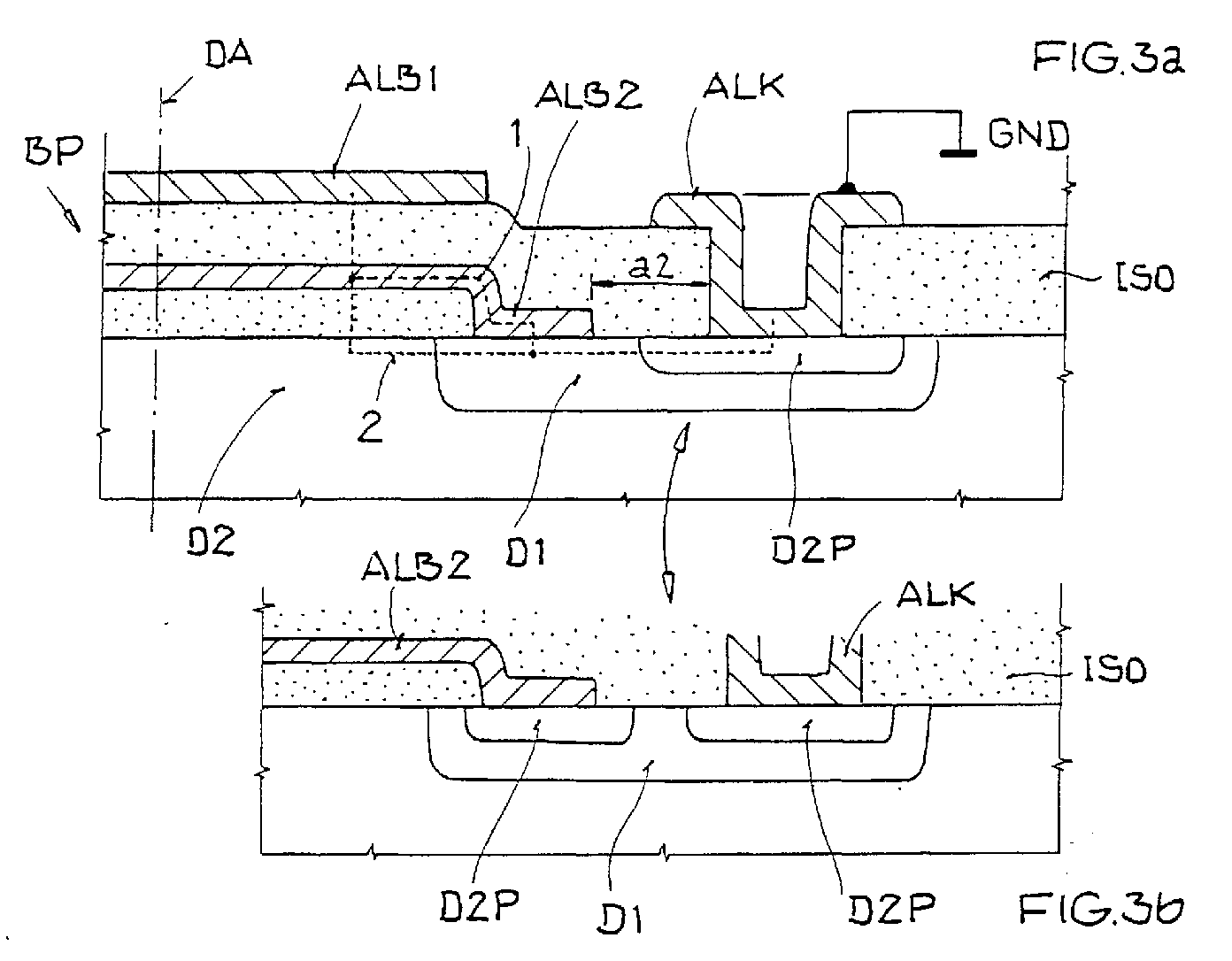
- the layer structure shown in FIG. 3a shows an arrangement for implementing the method according to the invention, with which the real and imaginary parts connected to the contact surface are greatly reduced within a customary manufacturing process of an integrated circuit, so that the physical parameters of the series resonant circuit change Determine contributions of the signal part ST.
- the axis DA is mirror-symmetrical.
- a second conductive layer ALB2 is introduced under the contact area ALB1 within the insulation layer, the size of which is adapted to the contact area ALB1 in order to achieve good shielding.
- the layer ALB2 is connected laterally to the zone D1 in order to produce a Schottky diode DALB2D1.
- Zone D1 completely encloses Zone D2P, which represents a connection doping for the contact ALK.
- the distance a2 between the contact ALK and the conductive layer ALB2 is significantly smaller and is in the range of approximately 1 ⁇ m.
- the total length of the zone D1 is determined from the width of the connection of the layer ALB2 and a distance a2 which results from the distance between the layer ALB2 and the connection of the reference potential ALK.
- the layer structure shown in FIG. 3b indicates an alternative embodiment in which the Schottky diode DALB2D1 from Figure 3a by a standard version of a diode DD2PD1 is replaced by below the contact area of the metallic conductive layer ALB2, another zone D2P is arranged.
- a conventional one is used Diode formed by the interface of zones D2P and zone D1. This is advantageous if training within the manufacturing process of the metallization process of a metal-semiconductor transition does not allow, but nevertheless good RF properties are needed.
- the Diode DD2PD1 Due to the small interface of the doping zones D2P and D1, the Diode DD2PD1 has a low capacitance. Furthermore, the length of zone D1 remains in Essentially unchanged.
- the equivalent circuit diagram corresponds to the HF description carried out in FIG. 3c the diode DD2PD1 that of the Schottky diode DALB2D1 from FIG. 3a.
- the HF equivalent circuit diagram shown in FIG. 3c describes the layer structure shown in FIG. 3a.
- the contact area ALB1 and the layer ALB2 form the capacitance C1A with the layer ISO.
- the series connection consists of current path 1 and current path 2.
- Current path 1 consists of the Schottky diode DALB2D1.
- the Schottky diode DALB2D1 consists of a capacitor C3A, which is connected in parallel with a resistor XRC3A and a resistor RS3A .., which is connected in series with the parallel circuit.
- the metal-semiconductor contact achieves a low capacitance value with high quality.
- the diode DD2D1 In the current path 2 there is a capacitance C2A, which is formed by the layer ALB2 and the zone D2 together with the zone ISO, in series with a resistor RSA, which is determined from the sheet resistance in zone D2, and in series with the diode DD2D1, which results from the interface of zones D1 / D2.
- the diode DD2D1 consists of a capacitor C4A, which is connected in parallel to a resistor XRC4A, and a resistor RSA4, which is connected in series with the parallel circuit. Both current paths lead through the layer D1, which has negligible resistance due to the small lateral expansion. Then the diode DD1D2P is in series.
- the diode DD1D2P consists of a capacitance C5A, which is connected in parallel to a resistor XRC5A, the parallel connection being a resistor RS5A in series and the capacitance C5A, due to the small interface and the high doping of the zone D2P, a small loss resistance and a high quality having.
- the contact ALK is represented by a resistor RS, the resistance of which is very small due to the metallically conductive layer. The mode of operation is explained below.
- the capacitance C3A which is derived from the equivalent circuit diagram of the Schottky diode, has a very small capacitance value in the range of a few fF.
- the real part ie the losses due to series resistance, is largely suppressed in current path 1, since both the contributions of the metallically conductive layers ALB2 and ALK are negligible, and the series resistance from the contribution of zone D1 is very low due to the very small distance a2 is.
- the small real part and imaginary part of the components located in current path 1 determine the contribution of the contact area to the real and imaginary parts of the series resonant circuit. Since the contributions of the contact area are extremely small, they can be neglected compared to the proportions given by the signal part ST of the integrated circuit IS.
Landscapes
- Engineering & Computer Science (AREA)
- Computer Hardware Design (AREA)
- Microelectronics & Electronic Packaging (AREA)
- Physics & Mathematics (AREA)
- General Physics & Mathematics (AREA)
- Theoretical Computer Science (AREA)
- Computer Networks & Wireless Communication (AREA)
- Semiconductor Integrated Circuits (AREA)
- Near-Field Transmission Systems (AREA)
- Variable-Direction Aerials And Aerial Arrays (AREA)
Abstract
Description
- Fig. 1
- ein HF-Ersatzschaltbild eines Eingangsteils eines Transponders, und
- Fig. 2a
- einen Querschnitt durch eine Kontaktfläche für einen Antennenanschluß innerhalb einer integrierten Halbleiteranordnung nach dem bisherigen Stand der Technik, und
- Fig. 2b
- das HF- Ersatzschaltbild der Kontaktfläche von der Fig. 2a, und
- Fig. 3a
- einen Querschnitt durch eine Kontaktfläche für einen Antennenanschluß, bei der die mit der Kontaktfläche verbundenen Real- und Imaginärteile mittels einer Schottky-Diodenanordnung unterdrückt werden, und
- Fig. 3b
- einen Querschnitt durch eine Kontaktfläche, bei der im Unterschied zu der Figur 3a die Schottky-Diodenanordnung durch eine herkömmlichen Diodendiodenanordnung ersetzt wird, und
- Fig. 3c
- das HF-Ersatzschaltbild für den in Figur 3a abgebildeten Querschnitt.
Im Folgenden wird der Aufbau des Querschnittbildes in Verbindung mit einer vereinfachten Wechselspannungsbetrachtung erläutert. Unter der Kontaktfläche ALB1 auf einem Halbleiterkörper aus Silizium, die in einer obersten Metallebene liegt, ist eine Isolationsschicht ISO ausgebildet, die die Kontaktfläche ALB1 von einer unterliegenden niedrig dotierten Zone D1 eines ersten Leitfähigkeittyps isoliert. Eine sich an die Zone D1 anschließende gering dotierte Zone D2 des zweiten Leitfähigkeittyps, die im Allgemeinen als Substratdotierung bezeichnet wird, kennzeichnet das Bezugspotential und ist mittels einer hochdotierten Zone D2P, des zweiten Leitfähigkeitstyps, an einen Kontakt ALK angeschlossen. Um eine ausreichende Prozesssicherheit bei der Herstellung der integrierten Schaltung IS zu gewährleisten, muß zwischen der Kontaktfläche ALB1 und dem Kontakt ALK ein großer Mindestabstand a1 eingehalten werden, der im Bereich von einigen 10 µm liegt, und die Länge der Zone D2 zwischen der Zone D1 und der Zone D2P bestimmt. In einer vereinfachten Wechselspannungsbetrachtung entspricht die Schichtenfolge aus der Kontaktfläche und der Zone D1 einem Kondensator mit einem Kapazitätsbelag CP, wobei die gering dotierte Zone D1 des zur Substratdotierung entgegengesetzten Leitfähigkeitstyps bewirkt, daß der kapazitive Beitrag CP der Kontaktflächen nicht sehr groß wird. In Serie zu dem Kondensator CP liegt ein Widerstand RP, der durch die große Länge der Zone D2 in Verbindung mit der geringen Dotierung einen hohen Wert aufweist.
Wie in Zusammenhang mit der Figur 2 erläutert, ist die Achse DA spiegelsymmetrisch. Im Folgenden wird der Aufbau erläutert, wobei aufbauend auf die in Zusammenhang mit der Figur 2 gemachten Erläuterungen nur die Unterschiede dargestellt werden. Unter der Kontaktfläche ALB1 wird innerhalb der Isolationsschicht eine zweite leitfähige Schicht ALB2 eingebracht, deren Größe der Kontaktfläche ALB1 angepaßt wird, um eine gute Abschirmung zu erreichen. Die Schicht ALB2 wird seitlich mit der Zone D1 verbunden, um damit eine Schottky-Diode DALB2D1 zu erzeugen. Die Zone D1 umschließt dabei die Zone D2P vollständig, die eine Anschlußdotierung für den Kontakt ALK darstellt. Im Unterschied zu dem Abstand a1 in Figur 2a, ist der Abstand a2 zwischen dem Kontakt ALK und der leitfähigen Schicht ALB2 wesentlich kleiner und liegt im Bereich etwa 1 µm. Die Gesamtlänge der Zone D1 bestimmt sich aus der Breite des Anschlusses der Schicht ALB2 und einem Abstand a2, der sich aus dem Abstand zwischen der Schicht ALB2 und dem Anschluß des Bezugspotentials ALK ergibt. Für die Beschreibung des Stromflusses in einem HF-Ersatzschaltbild wird zwischen einem ersten Strompfad 1 und einem zweiten Strompfad 2 unterschieden, die zueinander parallel geschaltet sind.
Im Folgenden wird die Funktionsweise erläutert. Um den Imaginärteil der Kontaktfläche, bestehend aus dem Beitrag der Kondensatoren zu unterdrücken, werden im Strompfad 1 der großen Kapazität C1A kleine Kapazitäten C3A und C5A mit größer Güte in Serie geschaltet werden. Insbesondere weist die Kapazität C3A, die sich aus dem Ersatzschaltbild der Schottky-Diode ableitet, einen sehr kleinen Kapazitätswert im Bereich von wenige fF auf. Ferner wird im Strompfad 1 auch der Realteil, d.h. die Verluste durch den Serienwiderstand weitestgehend unterdrückt, da sowohl die Beiträge der metallisch leitfähigen Schichten ALB2 und ALK vernachlässigbar sind, als auch der Serienwiderstand aus dem Beitrag der Zone D1 aufgrund des sehr kleinen Abstand a2 sehr gering ist. Ferner wird erreicht, daß im Strompfad 2, durch eine niedrige Dotierung der Serienwiderstand RSA im Vergleich zu den im Strompfad 1 vorliegenden Serienwiderstand der metallisch leitfähigen Schicht ALB2 groß ist. Da der Pfad 2 parallel zu dem Pfad 1 liegt, wird der relativ große Realteil des Strompfades 2 jedoch unterdrückt. Ferner ist durch die niedrige Dotierung der Zonen D1 und D2 die Kapazität des Kondensators C4A trotz der relativ großen Grenzfläche klein und weist gleichzeitig eine im Vergleich zu der aus der Schottky-Diode resultierenden Kapazität C3A eine sehr schlechte Güte auf. Damit wird der Beitrag zu dem Imaginärteil durch den Strompfad 2 unterdrückt. Der über den Strompfad 2 fließende HF-Strom ist damit vernachlässigbar. Insgesamt bestimmen damit die kleinen Realteil und Imaginärteil der im Strompfad 1 liegenden Bauelemete den Beitrag der Kontaktfläche zu den Real- und Imaginärteilen des Serienschwingkreis. Da die Beiträge der Kontaktfläche äußert klein sind, können diese jedoch gegenüber den Anteilen gegeben durch den Signalteil ST der integrierten Schaltung IS vernachlässigt werden.
Claims (7)
- Verfahren zum Abgleich eines Antennenschwingkreises eines passiven Transponders, dessen Betriebsenergie aus einem hochfrequenten elektromagnetischen Trägerfeld kapazitiv entnommen wird, unddadurch gekennzeichnet, daßder einen Halbleiterkörper mit einer integrierten Schaltung (IS) mit einem Signalteil (ST) mit Bezugspotentialanschluß aufweist,der einen auf einem Träger angeordnete Antennenanordnung aufweist,die Antennenanordnung über eine auf dem Halbleiterkörper angeschlossene Kontaktfläche (BP) mit der integrierten Schaltung (IS) verbunden ist,bei dem die Antenne (AN) mit der Eingangskapazität der integrierten Schaltung (IS) einen seriellen Schwingkreis bildet,
zur Erhöhung der Güte des Antennenschwingkreises die parasitären kapazitiven und resistiven Anteile, die einen Strompfad zwischen der Kontaktfläche (BP) und dem Bezugspotential bilden, reduziert werden. - Verfahren nach Anspruch 1, dadurch gekennzeichnet, daß der Strompfad an wenigstens einer Stelle, mittels einer Hintereinanderschaltung und Parallelschaltung von kapazitiven und resistiven Anteilen, in einen ersten Strompfad und einen zweiten Strompfad aufgeteilt wird.
- Verfahren nach Anspruch 2, dadurch gekennzeichnet, daß eine erste Kapazität mit hoher Güte und eine Parallelschaltung, von einer kleinen Kapazität, deren Kapazitätswert vorzugsweise im Bereich von einigen fF liegt, mit geringer Güte und einer kleinen Kapazität, deren Kapazitätswert vorzugsweise im Bereich von einigen fF liegt, mit hoher Güte, in Reihe geschaltet wird.
- Verfahren nach Anspruch 3, dadurch gekennzeichnet, daß die kleinen Kapazitäten mittels Dioden erzeugt werden.
- Verfahren nach Anspruch 3, dadurch gekennzeichnet, daß in einer unter der Kontaktfläche (BP) liegenden Isolationsschicht (ISO) eine leitfähige Schicht (ALB2) eingezogen wird, die zusammen mit der Kontaktfläche (BP) einen Kondensator mit hoher Güte bildet.
- Halbleiteranordnung zur Umsetzung des erfindungsgemäßen Verfahrens nach einem der Ansprüche 1 bis 5 mit einer ersten leitfähigen Schicht (ALB1) als Kontaktfläche (BP), zur Verbindung einer Antenne (AN) mit einer integrierten Schaltung (IS), einer Isolationsschicht (ISO), einer ersten Zone (D1) eines ersten Leitfähigkeitstyps, einer zweiten Zone (D2) eines zweiten Leitfähigkeitstyps und einer dritten hochdotierten Zone (D2P) des zweiten Leitfähigkeitstyps, die einen Kontakt (ALK), der ein Bezugspotential darstellt, mit dem Halbleitersubstrat verbindet,dadurch gekennzeichnet, daßinnerhalb der Isolationsschicht (ISO) eine weitere leitfähige Schicht (ALB2) angeordnet ist, deren laterale Ausdehnung größer als die Ausdehnung der Schicht (ALB1) ist, unddie Schicht (ALB2) eine Verbindung mit der ersten Zone (D1) aufweist, um eine Schottky-Diode zu bilden, unddie ersten Zone (D1) die dritte Zone (D2P) umschließt.
- Halbleiteranordnung nach Anspruch 6,dadurch gekennzeichnet, daßunter dem Anschlußbereich der Schicht (ALB2) eine vierte Zone (D2PP), des zweiten Leitfähigkeitstyps angeordnet ist, die von der ersten Zone (D1) umschlossen wird.
Applications Claiming Priority (2)
| Application Number | Priority Date | Filing Date | Title |
|---|---|---|---|
| DE10124222 | 2001-05-18 | ||
| DE10124222A DE10124222A1 (de) | 2001-05-18 | 2001-05-18 | Verfahren zum Abgleich eines Antennenschwingkreises eines passiven Transponders |
Publications (3)
| Publication Number | Publication Date |
|---|---|
| EP1258830A2 true EP1258830A2 (de) | 2002-11-20 |
| EP1258830A3 EP1258830A3 (de) | 2002-12-11 |
| EP1258830B1 EP1258830B1 (de) | 2008-08-27 |
Family
ID=7685248
Family Applications (1)
| Application Number | Title | Priority Date | Filing Date |
|---|---|---|---|
| EP02010096A Expired - Lifetime EP1258830B1 (de) | 2001-05-18 | 2002-05-07 | Verfahren zum Abgleich eines Antennenschwingkreises eines passiven Transponders |
Country Status (4)
| Country | Link |
|---|---|
| US (1) | US6952560B2 (de) |
| EP (1) | EP1258830B1 (de) |
| JP (1) | JP4098562B2 (de) |
| DE (2) | DE10124222A1 (de) |
Families Citing this family (16)
| Publication number | Priority date | Publication date | Assignee | Title |
|---|---|---|---|---|
| US7358848B2 (en) | 2002-11-19 | 2008-04-15 | Farrokh Mohamadi | Wireless remote sensor |
| US6885344B2 (en) | 2002-11-19 | 2005-04-26 | Farrokh Mohamadi | High-frequency antenna array |
| US6963307B2 (en) | 2002-11-19 | 2005-11-08 | Farrokh Mohamadi | Inductively-coupled antenna array |
| US7398054B2 (en) | 2003-08-29 | 2008-07-08 | Zih Corp. | Spatially selective UHF near field microstrip coupler device and RFID systems using device |
| KR100621370B1 (ko) * | 2004-06-08 | 2006-09-08 | 삼성전자주식회사 | 쇼트키 다이오드를 포함한 집적회로구조물 및 그 제조방법 |
| US8596532B2 (en) * | 2004-06-10 | 2013-12-03 | Zih Corp. | Apparatus and method for communicating with an RFID transponder |
| US7549591B2 (en) * | 2004-06-28 | 2009-06-23 | International Barcode Corporation | Combined multi-frequency electromagnetic and optical communication system |
| US7284704B2 (en) * | 2004-06-28 | 2007-10-23 | International Barcode Corporation | Combined electromagnetic and optical communication system |
| DE102004038528A1 (de) * | 2004-08-07 | 2006-03-16 | Atmel Germany Gmbh | Halbleiterstruktur |
| US7545272B2 (en) | 2005-02-08 | 2009-06-09 | Therasense, Inc. | RF tag on test strips, test strip vials and boxes |
| EP2341463A3 (de) * | 2007-04-19 | 2014-06-11 | BALLUFF GmbH | Datenträger-/Sendevorrichtung und Verfahren zu ihrer Herstellung |
| US9319756B2 (en) * | 2008-03-24 | 2016-04-19 | Intermec Ip Corp. | RFID tag communication triggered by sensed energy |
| US8559869B2 (en) | 2011-09-21 | 2013-10-15 | Daniel R. Ash, JR. | Smart channel selective repeater |
| TWI517613B (zh) * | 2013-10-17 | 2016-01-11 | 國立交通大學 | 非接觸式訊號傳輸整合式裝置 |
| WO2018126247A2 (en) | 2017-01-02 | 2018-07-05 | Mojoose, Inc. | Automatic signal strength indicator and automatic antenna switch |
| US11809926B2 (en) | 2020-02-04 | 2023-11-07 | Fujifilm Corporation | Noncontact communication medium, magnetic tape cartridge, and manufacturing method of noncontact communication medium |
Family Cites Families (11)
| Publication number | Priority date | Publication date | Assignee | Title |
|---|---|---|---|---|
| US5583819A (en) * | 1995-01-27 | 1996-12-10 | Single Chip Holdings, Inc. | Apparatus and method of use of radiofrequency identification tags |
| DE19614455A1 (de) * | 1996-04-12 | 1997-10-16 | Philips Patentverwaltung | Verfahren zum Betrieb eines Systems aus einer Basisstation und einem damit kontaktlos gekoppelten Transponders sowie dafür geeignetes System |
| DE19628802A1 (de) * | 1996-07-17 | 1998-01-22 | Telesensomatic Gmbh | Transponder |
| ZA981382B (en) * | 1997-03-07 | 1998-08-24 | Kaba Schliesssysteme Ag | High frequency identification medium with passive electronic data carrier |
| DE19755250A1 (de) * | 1997-12-12 | 1999-07-01 | Philips Patentverwaltung | Schaltungsanordnung zum Einstellen der Resonanzfrequenz |
| US6281794B1 (en) * | 1998-01-02 | 2001-08-28 | Intermec Ip Corp. | Radio frequency transponder with improved read distance |
| DE19811489B4 (de) * | 1998-03-17 | 2006-01-12 | Atmel Germany Gmbh | Portabler Hochfrequenzsender |
| DE19818968C2 (de) * | 1998-04-28 | 2000-11-30 | Fraunhofer Ges Forschung | Verfahren zur Herstellung eines Transponders, Verfahren zur Herstellung einer Chipkarte, die einen Transponder aufweist, sowie nach dem erfindungsgemäßen Verfahren hergestellter Transponder und nach dem erfindungsgemäßen Verfahren hergestellte Chipkarte |
| US6229442B1 (en) | 2000-03-14 | 2001-05-08 | Motorola, Inc, | Radio frequency identification device having displacement current control and method thereof |
| US6229443B1 (en) * | 2000-06-23 | 2001-05-08 | Single Chip Systems | Apparatus and method for detuning of RFID tag to regulate voltage |
| US6424315B1 (en) * | 2000-08-02 | 2002-07-23 | Amkor Technology, Inc. | Semiconductor chip having a radio-frequency identification transceiver |
-
2001
- 2001-05-18 DE DE10124222A patent/DE10124222A1/de not_active Withdrawn
-
2002
- 2002-05-07 EP EP02010096A patent/EP1258830B1/de not_active Expired - Lifetime
- 2002-05-07 DE DE50212694T patent/DE50212694D1/de not_active Expired - Lifetime
- 2002-05-13 US US10/145,160 patent/US6952560B2/en not_active Expired - Lifetime
- 2002-05-16 JP JP2002141935A patent/JP4098562B2/ja not_active Expired - Fee Related
Also Published As
| Publication number | Publication date |
|---|---|
| US6952560B2 (en) | 2005-10-04 |
| EP1258830B1 (de) | 2008-08-27 |
| US20020171602A1 (en) | 2002-11-21 |
| DE10124222A1 (de) | 2002-11-21 |
| JP4098562B2 (ja) | 2008-06-11 |
| JP2003051759A (ja) | 2003-02-21 |
| EP1258830A3 (de) | 2002-12-11 |
| DE50212694D1 (de) | 2008-10-09 |
Similar Documents
| Publication | Publication Date | Title |
|---|---|---|
| EP1258830B1 (de) | Verfahren zum Abgleich eines Antennenschwingkreises eines passiven Transponders | |
| EP1164532B1 (de) | Vorrichtung zur kontaktlosen Übertragung von Daten | |
| DE10158442B4 (de) | Sende- und Empfangseinrichtung für eine kontaktlose Datenübertragung | |
| DE102006054078B4 (de) | Breitbandantenne | |
| EP0826190B1 (de) | Kontaktlose chipkarte | |
| DE3850729T2 (de) | Monolithischer integrierter Mikrowellenverstärker. | |
| DE102013111027A1 (de) | Mehrfrequenzfähige Antenne für miniaturisierte Anwendungen | |
| DE102013102051A1 (de) | Boosterantenne, Kontaktlos-Chip-Anordnung, Antennenstruktur, und Chip-Anordnung | |
| DE102022104413A1 (de) | Antennenvorrichtung und antennenmodul mit dieser vorrichtung | |
| EP2003659A1 (de) | Monolithisch integrierte Induktivität | |
| DE69630558T2 (de) | Elektronisches Bauelement für eine kontaktlose passive Karte | |
| EP3001561B1 (de) | Antennenschaltung für nahfeld-antennen | |
| EP1489733B1 (de) | Gleichrichterschaltung für Transponder | |
| DE2512870A1 (de) | Resonanzkreis mit einem element mit veraenderbarer kapazitaet | |
| EP1983467B1 (de) | Datenträger-/Sendevorrichtung und Verfahren zu ihrer Herstellung | |
| DE102005037877A1 (de) | Diodenmischer | |
| EP1641041B1 (de) | Kondensatoranordnung unter einem Löthöcker | |
| EP1298757A1 (de) | Bandpassfilter für ein Hochfrequenzsignal und Abstimmverfahren dafür | |
| WO2020249753A1 (de) | Gleichrichter für millimeter-wellen-wechselspannungssignale | |
| EP1487052B1 (de) | Antennenanordnung in der Apertur einer elektrisch leitenden Fahrzeug-Karosserie | |
| DE102018211016A1 (de) | Schaltung zur signaltechnischen Verbindung, Vorrichtung zur induktiven Übertragung von Energie sowie zur Signalübertragung sowie Verfahren zur Herstellung | |
| DE10141583A1 (de) | Antennenanordnung in der Apertur einer elektrisch leitenden Fahrzeugkarosserie | |
| DE102005035346A1 (de) | Verlustleistungsoptimierter Hochfrequenz-Koppelkondensator und Gleichrichterschaltung | |
| DE102013102052B4 (de) | Chip-Anordnung | |
| EP3493324B1 (de) | Aktive multiband-antenne für den terrestrischen rundfunkempfang |
Legal Events
| Date | Code | Title | Description |
|---|---|---|---|
| PUAI | Public reference made under article 153(3) epc to a published international application that has entered the european phase |
Free format text: ORIGINAL CODE: 0009012 |
|
| PUAL | Search report despatched |
Free format text: ORIGINAL CODE: 0009013 |
|
| AK | Designated contracting states |
Kind code of ref document: A2 Designated state(s): AT BE CH CY DE DK ES FI FR GB GR IE IT LI LU MC NL PT SE TR |
|
| AX | Request for extension of the european patent |
Free format text: AL;LT;LV;MK;RO;SI |
|
| AK | Designated contracting states |
Kind code of ref document: A3 Designated state(s): AT BE CH CY DE DK ES FI FR GB GR IE IT LI LU MC NL PT SE TR |
|
| AX | Request for extension of the european patent |
Free format text: AL;LT;LV;MK;RO;SI |
|
| 17P | Request for examination filed |
Effective date: 20021107 |
|
| AKX | Designation fees paid |
Designated state(s): DE FI FR GB IT SE |
|
| 17Q | First examination report despatched |
Effective date: 20071011 |
|
| GRAP | Despatch of communication of intention to grant a patent |
Free format text: ORIGINAL CODE: EPIDOSNIGR1 |
|
| GRAS | Grant fee paid |
Free format text: ORIGINAL CODE: EPIDOSNIGR3 |
|
| GRAA | (expected) grant |
Free format text: ORIGINAL CODE: 0009210 |
|
| AK | Designated contracting states |
Kind code of ref document: B1 Designated state(s): DE FI FR GB IT SE |
|
| REG | Reference to a national code |
Ref country code: GB Ref legal event code: FG4D Free format text: NOT ENGLISH |
|
| REF | Corresponds to: |
Ref document number: 50212694 Country of ref document: DE Date of ref document: 20081009 Kind code of ref document: P |
|
| PG25 | Lapsed in a contracting state [announced via postgrant information from national office to epo] |
Ref country code: FI Free format text: LAPSE BECAUSE OF FAILURE TO SUBMIT A TRANSLATION OF THE DESCRIPTION OR TO PAY THE FEE WITHIN THE PRESCRIBED TIME-LIMIT Effective date: 20080827 |
|
| PLBE | No opposition filed within time limit |
Free format text: ORIGINAL CODE: 0009261 |
|
| STAA | Information on the status of an ep patent application or granted ep patent |
Free format text: STATUS: NO OPPOSITION FILED WITHIN TIME LIMIT |
|
| 26N | No opposition filed |
Effective date: 20090528 |
|
| PG25 | Lapsed in a contracting state [announced via postgrant information from national office to epo] |
Ref country code: IT Free format text: LAPSE BECAUSE OF FAILURE TO SUBMIT A TRANSLATION OF THE DESCRIPTION OR TO PAY THE FEE WITHIN THE PRESCRIBED TIME-LIMIT Effective date: 20080827 |
|
| GBPC | Gb: european patent ceased through non-payment of renewal fee |
Effective date: 20090507 |
|
| PG25 | Lapsed in a contracting state [announced via postgrant information from national office to epo] |
Ref country code: SE Free format text: LAPSE BECAUSE OF FAILURE TO SUBMIT A TRANSLATION OF THE DESCRIPTION OR TO PAY THE FEE WITHIN THE PRESCRIBED TIME-LIMIT Effective date: 20081127 |
|
| REG | Reference to a national code |
Ref country code: FR Ref legal event code: ST Effective date: 20100129 |
|
| PG25 | Lapsed in a contracting state [announced via postgrant information from national office to epo] |
Ref country code: FR Free format text: LAPSE BECAUSE OF NON-PAYMENT OF DUE FEES Effective date: 20090602 |
|
| PG25 | Lapsed in a contracting state [announced via postgrant information from national office to epo] |
Ref country code: GB Free format text: LAPSE BECAUSE OF NON-PAYMENT OF DUE FEES Effective date: 20090507 |
|
| PGFP | Annual fee paid to national office [announced via postgrant information from national office to epo] |
Ref country code: DE Payment date: 20120529 Year of fee payment: 11 |
|
| REG | Reference to a national code |
Ref country code: DE Ref legal event code: R082 Ref document number: 50212694 Country of ref document: DE Representative=s name: GRUENECKER, KINKELDEY, STOCKMAIR & SCHWANHAEUS, DE Effective date: 20130529 Ref country code: DE Ref legal event code: R081 Ref document number: 50212694 Country of ref document: DE Owner name: ATMEL CORP., US Free format text: FORMER OWNER: ATMEL AUTOMOTIVE GMBH, 74072 HEILBRONN, DE Effective date: 20130529 |
|
| PG25 | Lapsed in a contracting state [announced via postgrant information from national office to epo] |
Ref country code: DE Free format text: LAPSE BECAUSE OF NON-PAYMENT OF DUE FEES Effective date: 20131203 |
|
| REG | Reference to a national code |
Ref country code: DE Ref legal event code: R119 Ref document number: 50212694 Country of ref document: DE Effective date: 20131203 |