EP1255288A2 - Bauelement auf GaAs und Herstellungsverfahren - Google Patents
Bauelement auf GaAs und Herstellungsverfahren Download PDFInfo
- Publication number
- EP1255288A2 EP1255288A2 EP02009028A EP02009028A EP1255288A2 EP 1255288 A2 EP1255288 A2 EP 1255288A2 EP 02009028 A EP02009028 A EP 02009028A EP 02009028 A EP02009028 A EP 02009028A EP 1255288 A2 EP1255288 A2 EP 1255288A2
- Authority
- EP
- European Patent Office
- Prior art keywords
- substrate
- gaas
- component
- thickness
- holes
- Prior art date
- Legal status (The legal status is an assumption and is not a legal conclusion. Google has not performed a legal analysis and makes no representation as to the accuracy of the status listed.)
- Withdrawn
Links
Images
Classifications
-
- H—ELECTRICITY
- H10—SEMICONDUCTOR DEVICES; ELECTRIC SOLID-STATE DEVICES NOT OTHERWISE PROVIDED FOR
- H10W—GENERIC PACKAGES, INTERCONNECTIONS, CONNECTORS OR OTHER CONSTRUCTIONAL DETAILS OF DEVICES COVERED BY CLASS H10
- H10W40/00—Arrangements for thermal protection or thermal control
- H10W40/20—Arrangements for cooling
- H10W40/22—Arrangements for cooling characterised by their shape, e.g. having conical or cylindrical projections
- H10W40/226—Arrangements for cooling characterised by their shape, e.g. having conical or cylindrical projections characterised by projecting parts, e.g. fins to increase surface area
- H10W40/228—Arrangements for cooling characterised by their shape, e.g. having conical or cylindrical projections characterised by projecting parts, e.g. fins to increase surface area the projecting parts being wire-shaped or pin-shaped
-
- H—ELECTRICITY
- H10—SEMICONDUCTOR DEVICES; ELECTRIC SOLID-STATE DEVICES NOT OTHERWISE PROVIDED FOR
- H10P—GENERIC PROCESSES OR APPARATUS FOR THE MANUFACTURE OR TREATMENT OF DEVICES COVERED BY CLASS H10
- H10P90/00—Preparation of wafers not covered by a single main group of this subclass, e.g. wafer reinforcement
- H10P90/12—Preparing bulk and homogeneous wafers
-
- H—ELECTRICITY
- H10—SEMICONDUCTOR DEVICES; ELECTRIC SOLID-STATE DEVICES NOT OTHERWISE PROVIDED FOR
- H10W—GENERIC PACKAGES, INTERCONNECTIONS, CONNECTORS OR OTHER CONSTRUCTIONAL DETAILS OF DEVICES COVERED BY CLASS H10
- H10W70/00—Package substrates; Interposers; Redistribution layers [RDL]
- H10W70/60—Insulating or insulated package substrates; Interposers; Redistribution layers
- H10W70/67—Insulating or insulated package substrates; Interposers; Redistribution layers characterised by their insulating layers or insulating parts
- H10W70/68—Shapes or dispositions thereof
Definitions
- the present invention relates to semiconductor devices in Gallium arsenide material system.
- GaAs material systems Semiconductor components, such as. B. transistors, MMICs (modularly mounted integrated circuits), HBTs (heterobipolar transistors) or HEMTs (high electron mobility transistors), in GaAs material systems have been known for a long time.
- a disadvantage is that this semiconductor material is a mixed crystal is extremely brittle and breaks easily, so that substrates and manufactured components according to careful handling require. Despite appropriate measures, the Manufacture of GaAs devices the yield of functional Components significantly restricted due to breakage.
- the object of the present invention is one possibility specify how semiconductor devices in the material system of GaAs with a higher yield of functional copies can be produced.
- a substrate is made of GaAs present, which has a thickness d of at most about 10 microns to has about 30 microns.
- the material has properties in this thickness a film, especially flexibility and Elasticity that prevents the substrate from breaking.
- a applied, e.g. B. evaporated or dusted, metallization may be present in certain embodiments to increase the tensile strength of the substrate and the flexibility to reduce to the desired extent, in particular, integrated semiconductor components present on the substrate not exposed to excessive mechanical stress become.
- the structure of a component provided with such a substrate can compared to conventional semiconductor devices be significantly improved since in a substrate the specified Thick extremely small holes for vias (via holes) can be etched in the form of so-called micro via holes can.
- the diameter of a micro via hole can be 1 ⁇ m or less.
- a vertical contact through the Through the substrate using electrically conductive contact hole fillings, which is introduced into these holes is thus easily possible even in very small dimensions.
- thermal properties of the components since the heat generated during operation is reduced by a thin one Substrate better on that facing away from the integrated device Side of the substrate can be dissipated.
- the lesser Dimension compared to previous semiconductor components and said good heat dissipation enable use smaller housing.
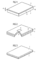
- a substrate 10 made of GaAs is original Thickness is shown on which in this example only one epitaxial grown layer 2 is present. It can multiple layers may be present depending on how it works of the component structured differently, with provided electrically conductive doped areas and contacts and by means of structured metallization levels to circuits can be wired. The details correspond known components and are not shown here.
- the substrate 1 of the invention Component up to a rear surface 3 (dashed drawn) to a thickness d of about 30 microns, preferably about 10 ⁇ m, thinned.
- Figure 2 shows another embodiment in which several grown layers 2, 21, 22 are present, the top is provided with a contact surface 5.
- This contact area 5 made of an electrically conductive material, preferably a metal, is over a contact hole 6, which is shown here in a sectional view, and in electrically conductive connection with an electrically conductive Contact hole filling, which is introduced into the contact hole 6 is.
- the material of the contact hole filling z. B. that too otherwise use tungsten used for this purpose, though the diameter of the contact hole 6 and thus the Diameter of the via formed with the contact hole filling is much lower than conventional ones undiluted components, preferably at most 1 ⁇ m.
- Figure 3 shows another embodiment in which the back the thinned with a grown layer 2
- Substrate 1 an evaporated or sputtered metallization 7 has.
- the component according to the invention is preferably manufactured by from a main side of a GaAs substrate at least one electrically doped in the substrate material Area is formed and / or on the substrate at least one layer of semiconductor material epitaxially is grown and then the substrate by thin grinding from the opposite main side to a thickness below of the specified values.
- the label Thin grinding also includes chemical mechanical Polishing (chemical-mechanical polishing, CMP) or lapping.
Landscapes
- Internal Circuitry In Semiconductor Integrated Circuit Devices (AREA)
- Electrodes Of Semiconductors (AREA)
- Mechanical Treatment Of Semiconductor (AREA)
Abstract
Ein Substrat (10) aus GaAs ist durch Dünnschleifen auf eine Dicke (d) von höchstens etwa 10 µm bis etwa 30 µm reduziert und besitzt Eigenschaften einer Folie, die ein Brechen des Substrates verhindern. Eine Metallisierung kann rückseitig auf das Substrat aufgebracht sein. Die thermischen Eigenschaften sind verbessert, da die Wärme besser auf die Rückseite des Substrates abgeführt werden kann. Die geringere Abmessung und die gute Wärmeableitung ermöglichen die Verwendung kleinerer Gehäuse. In das Substrat können äußerst kleine Löcher (micro via holes) geätzt und mit Kontaktlochfüllungen versehen sein. <IMAGE>
Description
Die vorliegende Erfindung betrifft Halbleiterbauelemente im
Materialsystem von Galliumarsenid.
Halbleiterbauelemente, wie z. B. Transistoren, MMICs (modularly
mounted integrated circuits), HBTs (Heterobipolartransistoren)
oder HEMTs (high electron mobility transistors), im
Materialsystem von GaAs sind seit langem bekannt. Von Nachteil
ist, dass dieses Halbleitermaterial als Mischkristall
extrem spröde ist und leicht bricht, so dass Substrate und
gefertigte Bauelemente einer entsprechend vorsichtigen Handhabung
bedürfen. Trotz entsprechender Maßnahmen ist bei der
Herstellung von GaAs-Bauelementen die Ausbeute an funktionsfähigen
Bauelementen infolge Bruchs erheblich eingeschränkt.
Aufgabe der vorliegenden Erfindung ist es, eine Möglichkeit
anzugeben, wie Halbleiterbauelemente im Materialsystem von
GaAs mit einer höheren Ausbeute an funktionsfähigen Exemplaren
hergestellt werden können.
Diese Aufgabe wird mit dem Bauelement mit den Merkmalen des
Anspruchs 1 bzw. mit dem Verfahren mit den Merkmalen des Anspruchs
5 gelöst. Ausgestaltungen ergeben sich aus den abhängigen
Ansprüchen.
Bei dem erfindungsgemäßen Bauelement ist ein Substrat aus
GaAs vorhanden, das eine Dicke d von höchstens etwa 10 µm bis
etwa 30 µm aufweist. In dieser Dicke besitzt das Material Eigenschaften
einer Folie, insbesondere eine Flexibilität und
Dehnbarkeit, die ein Brechen des Substrates verhindern. Eine
aufgebrachte, z. B. aufgedampfte oder aufgestäubte, Metallisierung
kann bei bestimmten Ausführungsformen vorhanden sein,
um die Reißfestigkeit des Substrates zu erhöhen und die Flexibilität
in gewünschtem Umfang zu vermindern, insbesondere,
damit auf dem Substrat vorhandene integrierte Halbleiterbauelemente
keinen zu großen mechanischen Spannungen ausgesetzt
werden.
Die Struktur eines mit einem solchen Substrat versehenen Bauelementes
kann gegenüber herkömmlichen Halbleiterbauelementen
deutlich verbessert sein, da in ein Substrat der angegebenen
Dicke äußerst kleine Löcher für Durchkontaktierungen (via holes)
in Gestalt von so genannten Micro Via Holes geätzt werden
können. Der Durchmesser eines Micro Via Holes kann 1 µm
oder weniger betragen. Eine vertikale Kontaktierung durch das
Substrat hindurch mittels elektrisch leitender Kontaktlochfüllungen,
die in diese Löcher eingebracht werden, ist somit
problemlos auch in sehr kleinen Dimensionen möglich. Ferner
ergeben sich verbesserte thermische Eigenschaften der Bauelemente,
da die im Betrieb entstehende Wärme durch ein dünnes
Substrat besser auf die von dem integrierten Bauelement abgewandte
Seite des Substrates abgeführt werden kann. Die geringere
Abmessung gegenüber bisherigen Halbleiterbauelementen
und die besagte gute Wärmeableitung ermöglichen die Verwendung
kleinerer Gehäuse.
Die beigefügten Figuren zeigen Beispiele für die Ausführungsformen
des Bauelementes.
In Figur 1 ist ein Substrat 10 aus GaAs in ursprünglicher
Dicke dargestellt, auf dem in diesem Beispiel nur eine epitaktisch
aufgewachsene Schicht 2 vorhanden ist. Es können
mehrere Schichten vorhanden sein, die je nach der Funktionsweise
des Bauelementes unterschiedlich strukturiert, mit
elektrisch leitend dotierten Bereichen und Kontakten versehen
und mittels strukturierter Metallisierungsebenen zu Schaltungen
verdrahtet sein können. Die Einzelheiten entsprechen an
sich bekannten Bauelementen und sind hier nicht dargestellt.
Von der Rückseite 4 ist das Substrat 1 des erfindungsgemäßen
Bauelementes bis zu einer rückseitigen Fläche 3 (gestrichelt
eingezeichnet) auf eine Dicke d von etwa 30 µm, vorzugsweise
etwa 10 µm, gedünnt.
Figur 2 zeigt ein anderes Ausführungsbeispiel, bei dem mehrere
aufgewachsene Schichten 2, 21, 22 vorhanden sind, deren
oberste mit einer Kontaktfläche 5 versehen ist. Diese Kontaktfläche
5 aus einem elektrisch leitenden Material, vorzugsweise
einem Metall, befindet sich über einem Kontaktloch
6, das hier in einer Schnittansicht dargestellt ist, und in
elektrisch leitender Verbindung mit einer elektrisch leitenden
Kontaktlochfüllung, die in das Kontaktloch 6 eingebracht
ist. Als Material der Kontaktlochfüllung kann z. B. das auch
sonst für diesen Zweck verwendete Wolfram dienen, wobei allerdings
der Durchmesser des Kontaktloches 6 und damit der
Durchmesser der mit der Kontaktlochfüllung gebildeten Durchkontaktierung
wesentlich geringer ist als bei herkömmlichen
ungedünnten Bauelementen, vorzugsweise höchstens 1 µm.
Figur 3 zeigt eine weitere Ausführungsform, bei der die Rückseite
des mit einer aufgewachsenen Schicht 2 versehenen gedünnten
Substrates 1 eine aufgedampfte oder aufgestäubte Metallisierung
7 aufweist.
Das erfindungsgemäße Bauelement wird vorzugsweise hergestellt,
indem von einer Hauptseite eines GaAs-Substrates her
in dem Substratmaterial mindestens ein elektrisch leitend dotierter
Bereich ausgebildet wird und/oder auf das Substrat
mindestens eine Schicht aus Halbleitermaterial epitaktisch
aufgewachsen wird und danach das Substrat durch Dünnschleifen
von der gegenüberliegenden Hauptseite her auf eine Dicke unterhalb
der angegebenen Werte gebracht wird. Die Bezeichnung
Dünnschleifen umfasst hierbei auch das chemisch-mechanische
Polieren (chemical-mechanical polishing, CMP) oder Läppen.
Bezugszeichenliste
- 1
- Substrat
- 2
- epitaktisch aufgewachsene Schicht
- 3
- rückseitige Fläche
- 4
- Rückseite
- 5
- Kontaktfläche
- 6
- Kontaktloch
- 7
- Metallisierung
- 10
- Substrat
- 21
- aufgewachsene Schicht
- 22
- aufgewachsene Schicht
Claims (6)
- Bauelement auf einem Substrat (1) aus GaAs, bei dem das Substrat eine Dicke (d) von höchstens 30 µm aufweist.
- Bauelement nach Anspruch 1, bei dem das Substrat (1) eine Dicke (d) von höchstens 10 µm aufweist.
- Bauelement nach Anspruch 1 oder 2, bei dem Löcher (6) in dem Substratmaterial mit einem Durchmesser von höchsten 1 µm vorhanden sind, die das Substrat (1) durchdringen.
- Bauelement nach Anspruch 3, bei dem die Löcher (6) mit elektrisch leitfähigem Material als Kontaktlochfüllung gefüllt sind.
- Verfahren zur Herstellung eines Bauelementes auf einem Substrat aus GaAs, bei dem von einer Hauptseite des Substrates (10) her
in dem Substrat mindestens ein elektrisch leitend dotierter Bereich ausgebildet wird und/oder auf das Substrat mindestens eine Schicht (2) aus Halbleitermaterial epitaktisch aufgewachsen wird und
das Substrat danach von der gegenüberliegenden Seite auf eine Dicke (d) von höchstens 30 µm gedünnt wird. - Verfahren nach Anspruch 5, bei dem
in das gedünnte Substrat (1) Löcher (6) geätzt werden, die als Durchkontaktierungen vorgesehen sind.
Applications Claiming Priority (2)
| Application Number | Priority Date | Filing Date | Title |
|---|---|---|---|
| DE10121549 | 2001-05-03 | ||
| DE10121549A DE10121549A1 (de) | 2001-05-03 | 2001-05-03 | Bauelement auf GaAs und Herstellungsverfahren |
Publications (1)
| Publication Number | Publication Date |
|---|---|
| EP1255288A2 true EP1255288A2 (de) | 2002-11-06 |
Family
ID=7683514
Family Applications (1)
| Application Number | Title | Priority Date | Filing Date |
|---|---|---|---|
| EP02009028A Withdrawn EP1255288A2 (de) | 2001-05-03 | 2002-04-23 | Bauelement auf GaAs und Herstellungsverfahren |
Country Status (4)
| Country | Link |
|---|---|
| US (1) | US20020163060A1 (de) |
| EP (1) | EP1255288A2 (de) |
| JP (1) | JP2003031793A (de) |
| DE (1) | DE10121549A1 (de) |
Families Citing this family (1)
| Publication number | Priority date | Publication date | Assignee | Title |
|---|---|---|---|---|
| US8397301B2 (en) * | 2009-11-18 | 2013-03-12 | Lookout, Inc. | System and method for identifying and assessing vulnerabilities on a mobile communication device |
Family Cites Families (1)
| Publication number | Priority date | Publication date | Assignee | Title |
|---|---|---|---|---|
| US5336930A (en) * | 1992-06-26 | 1994-08-09 | The United States Of America As Represented By The Secretary Of The Air Force | Backside support for thin wafers |
-
2001
- 2001-05-03 DE DE10121549A patent/DE10121549A1/de not_active Withdrawn
-
2002
- 2002-04-23 EP EP02009028A patent/EP1255288A2/de not_active Withdrawn
- 2002-05-03 US US10/138,653 patent/US20020163060A1/en not_active Abandoned
- 2002-05-07 JP JP2002132019A patent/JP2003031793A/ja active Pending
Also Published As
| Publication number | Publication date |
|---|---|
| US20020163060A1 (en) | 2002-11-07 |
| DE10121549A1 (de) | 2002-11-14 |
| JP2003031793A (ja) | 2003-01-31 |
Similar Documents
| Publication | Publication Date | Title |
|---|---|---|
| EP0610709B1 (de) | Verfahren zur Herstellung einer dreidimensionalen Schaltungsanordnung | |
| DE10245631B4 (de) | Halbleiterbauelement | |
| DE112014007341B4 (de) | GaN-TRANSISTOREN MIT POLYSILIZIUMSCHICHTEN ZUR BILDUNG VON ZUSÄTZLICHEN KOMPONENTEN UND VERFAHREN ZU DEREN HERSTELLUNG | |
| DE102004059657B4 (de) | Diamanthalbleitervorrichtung und Verfahren zu dessen Herstellung | |
| DE102011053362B4 (de) | Vorrichtung und Verfahren zu deren Herstellung | |
| DE102004052921A1 (de) | Verfahren zur Herstellung von Halbleiterbauelementen mit externen Kontaktierungen | |
| DE112012000612T5 (de) | lonenimplantierte und selbstjustierende Gate-Struktur für GaN-Transistoren | |
| EP0575789B1 (de) | Monolithisch integrierter Millimeterwellenschaltkreis und Verfahren zu dessen Herstellung | |
| DE112021000892T5 (de) | Halbleiterbauteil, ein dieses aufweisendes halbleitergehäuse, und verfahren zur herstellung eines halbleiterbauteils | |
| DE69524730T2 (de) | Verfahren zur Herstellung einer Halbleitervorrichtung für Mikrowellen | |
| DE102014107560A1 (de) | Halbleiterbauelement und Verfahren | |
| DE102017109670B4 (de) | Herstellungsverfahren für ein Chippackage mit Seitenwandmetallisierung | |
| EP0293630A1 (de) | Halbleiterkörper mit Wärmesenke | |
| DE10324751B4 (de) | Verfahren zur Herstellung einer Halbleiter-Struktur mit einem Halbleitersubstrat und mit diesem Verfahren hergestellte Halbleiter-Struktur | |
| EP1393383B1 (de) | Laterale pin-diode und verfahren zur herstellung derselben | |
| DE69230514T2 (de) | Verfahren zur Herstellung eines vergrabenen Kontaktes aus Polysilizium | |
| DE69113725T2 (de) | Leistungstransistor und Verfahren zur Herstellung. | |
| DE69008693T2 (de) | Methode zur Herstellung eines Halbleiterbauelementes mit angeschrägten Öffnungen. | |
| EP1255288A2 (de) | Bauelement auf GaAs und Herstellungsverfahren | |
| DE69327012T2 (de) | Bauelement mit einer räumlichen Transfer verwendenden Halbleiteranordnung | |
| DE112023002581T5 (de) | Kantenemittierende halbleiterlaserdiode; verfahren zur herstellung eines halbleiterbauelements und halbleiterlaserbauelement | |
| DE69333124T2 (de) | Halbleiteranordnung und Schaltung | |
| DE112022006142T5 (de) | Halbleitervorrichtung und elektroleistungsumwandlungsvorrichtung | |
| DE102009043740A1 (de) | Rückseitenmetallisierung mit besserer Haftung in Hochleistungshalbleiterbauelementen | |
| DE102004036962A1 (de) | Verfahren zur Herstellung von Halbleiterchips in Dünnfilmtechnik und Halbleiterchip in Dünnfilmtechnik |
Legal Events
| Date | Code | Title | Description |
|---|---|---|---|
| PUAI | Public reference made under article 153(3) epc to a published international application that has entered the european phase |
Free format text: ORIGINAL CODE: 0009012 |
|
| AK | Designated contracting states |
Kind code of ref document: A2 Designated state(s): AT BE CH CY DE DK ES FI FR GB GR IE IT LI LU MC NL PT SE TR |
|
| AX | Request for extension of the european patent |
Free format text: AL;LT;LV;MK;RO;SI |
|
| RAP1 | Party data changed (applicant data changed or rights of an application transferred) |
Owner name: TRIQUINT SEMICONDUCTOR GMBH |
|
| STAA | Information on the status of an ep patent application or granted ep patent |
Free format text: STATUS: THE APPLICATION IS DEEMED TO BE WITHDRAWN |
|
| 18D | Application deemed to be withdrawn |
Effective date: 20041102 |