EP1255154A2 - Liquid crystal display device and method of fabricating the same - Google Patents
Liquid crystal display device and method of fabricating the same Download PDFInfo
- Publication number
- EP1255154A2 EP1255154A2 EP02009485A EP02009485A EP1255154A2 EP 1255154 A2 EP1255154 A2 EP 1255154A2 EP 02009485 A EP02009485 A EP 02009485A EP 02009485 A EP02009485 A EP 02009485A EP 1255154 A2 EP1255154 A2 EP 1255154A2
- Authority
- EP
- European Patent Office
- Prior art keywords
- liquid crystal
- retardation plate
- retardation
- transparent substrate
- display device
- Prior art date
- Legal status (The legal status is an assumption and is not a legal conclusion. Google has not performed a legal analysis and makes no representation as to the accuracy of the status listed.)
- Granted
Links
Images


Classifications
-
- G—PHYSICS
- G02—OPTICS
- G02F—OPTICAL DEVICES OR ARRANGEMENTS FOR THE CONTROL OF LIGHT BY MODIFICATION OF THE OPTICAL PROPERTIES OF THE MEDIA OF THE ELEMENTS INVOLVED THEREIN; NON-LINEAR OPTICS; FREQUENCY-CHANGING OF LIGHT; OPTICAL LOGIC ELEMENTS; OPTICAL ANALOGUE/DIGITAL CONVERTERS
- G02F1/00—Devices or arrangements for the control of the intensity, colour, phase, polarisation or direction of light arriving from an independent light source, e.g. switching, gating or modulating; Non-linear optics
- G02F1/01—Devices or arrangements for the control of the intensity, colour, phase, polarisation or direction of light arriving from an independent light source, e.g. switching, gating or modulating; Non-linear optics for the control of the intensity, phase, polarisation or colour
- G02F1/13—Devices or arrangements for the control of the intensity, colour, phase, polarisation or direction of light arriving from an independent light source, e.g. switching, gating or modulating; Non-linear optics for the control of the intensity, phase, polarisation or colour based on liquid crystals, e.g. single liquid crystal display cells
- G02F1/133—Constructional arrangements; Operation of liquid crystal cells; Circuit arrangements
- G02F1/1333—Constructional arrangements; Manufacturing methods
- G02F1/1335—Structural association of cells with optical devices, e.g. polarisers or reflectors
- G02F1/133553—Reflecting elements
- G02F1/133555—Transflectors
-
- G—PHYSICS
- G02—OPTICS
- G02F—OPTICAL DEVICES OR ARRANGEMENTS FOR THE CONTROL OF LIGHT BY MODIFICATION OF THE OPTICAL PROPERTIES OF THE MEDIA OF THE ELEMENTS INVOLVED THEREIN; NON-LINEAR OPTICS; FREQUENCY-CHANGING OF LIGHT; OPTICAL LOGIC ELEMENTS; OPTICAL ANALOGUE/DIGITAL CONVERTERS
- G02F1/00—Devices or arrangements for the control of the intensity, colour, phase, polarisation or direction of light arriving from an independent light source, e.g. switching, gating or modulating; Non-linear optics
- G02F1/01—Devices or arrangements for the control of the intensity, colour, phase, polarisation or direction of light arriving from an independent light source, e.g. switching, gating or modulating; Non-linear optics for the control of the intensity, phase, polarisation or colour
- G02F1/13—Devices or arrangements for the control of the intensity, colour, phase, polarisation or direction of light arriving from an independent light source, e.g. switching, gating or modulating; Non-linear optics for the control of the intensity, phase, polarisation or colour based on liquid crystals, e.g. single liquid crystal display cells
- G02F1/133—Constructional arrangements; Operation of liquid crystal cells; Circuit arrangements
- G02F1/1333—Constructional arrangements; Manufacturing methods
- G02F1/1335—Structural association of cells with optical devices, e.g. polarisers or reflectors
- G02F1/13363—Birefringent elements, e.g. for optical compensation
-
- G—PHYSICS
- G02—OPTICS
- G02F—OPTICAL DEVICES OR ARRANGEMENTS FOR THE CONTROL OF LIGHT BY MODIFICATION OF THE OPTICAL PROPERTIES OF THE MEDIA OF THE ELEMENTS INVOLVED THEREIN; NON-LINEAR OPTICS; FREQUENCY-CHANGING OF LIGHT; OPTICAL LOGIC ELEMENTS; OPTICAL ANALOGUE/DIGITAL CONVERTERS
- G02F1/00—Devices or arrangements for the control of the intensity, colour, phase, polarisation or direction of light arriving from an independent light source, e.g. switching, gating or modulating; Non-linear optics
- G02F1/01—Devices or arrangements for the control of the intensity, colour, phase, polarisation or direction of light arriving from an independent light source, e.g. switching, gating or modulating; Non-linear optics for the control of the intensity, phase, polarisation or colour
- G02F1/13—Devices or arrangements for the control of the intensity, colour, phase, polarisation or direction of light arriving from an independent light source, e.g. switching, gating or modulating; Non-linear optics for the control of the intensity, phase, polarisation or colour based on liquid crystals, e.g. single liquid crystal display cells
- G02F1/133—Constructional arrangements; Operation of liquid crystal cells; Circuit arrangements
- G02F1/1333—Constructional arrangements; Manufacturing methods
- G02F1/1335—Structural association of cells with optical devices, e.g. polarisers or reflectors
- G02F1/133553—Reflecting elements
-
- G—PHYSICS
- G02—OPTICS
- G02F—OPTICAL DEVICES OR ARRANGEMENTS FOR THE CONTROL OF LIGHT BY MODIFICATION OF THE OPTICAL PROPERTIES OF THE MEDIA OF THE ELEMENTS INVOLVED THEREIN; NON-LINEAR OPTICS; FREQUENCY-CHANGING OF LIGHT; OPTICAL LOGIC ELEMENTS; OPTICAL ANALOGUE/DIGITAL CONVERTERS
- G02F1/00—Devices or arrangements for the control of the intensity, colour, phase, polarisation or direction of light arriving from an independent light source, e.g. switching, gating or modulating; Non-linear optics
- G02F1/01—Devices or arrangements for the control of the intensity, colour, phase, polarisation or direction of light arriving from an independent light source, e.g. switching, gating or modulating; Non-linear optics for the control of the intensity, phase, polarisation or colour
- G02F1/13—Devices or arrangements for the control of the intensity, colour, phase, polarisation or direction of light arriving from an independent light source, e.g. switching, gating or modulating; Non-linear optics for the control of the intensity, phase, polarisation or colour based on liquid crystals, e.g. single liquid crystal display cells
- G02F1/133—Constructional arrangements; Operation of liquid crystal cells; Circuit arrangements
- G02F1/1333—Constructional arrangements; Manufacturing methods
- G02F1/133371—Cells with varying thickness of the liquid crystal layer
-
- G—PHYSICS
- G02—OPTICS
- G02F—OPTICAL DEVICES OR ARRANGEMENTS FOR THE CONTROL OF LIGHT BY MODIFICATION OF THE OPTICAL PROPERTIES OF THE MEDIA OF THE ELEMENTS INVOLVED THEREIN; NON-LINEAR OPTICS; FREQUENCY-CHANGING OF LIGHT; OPTICAL LOGIC ELEMENTS; OPTICAL ANALOGUE/DIGITAL CONVERTERS
- G02F1/00—Devices or arrangements for the control of the intensity, colour, phase, polarisation or direction of light arriving from an independent light source, e.g. switching, gating or modulating; Non-linear optics
- G02F1/01—Devices or arrangements for the control of the intensity, colour, phase, polarisation or direction of light arriving from an independent light source, e.g. switching, gating or modulating; Non-linear optics for the control of the intensity, phase, polarisation or colour
- G02F1/13—Devices or arrangements for the control of the intensity, colour, phase, polarisation or direction of light arriving from an independent light source, e.g. switching, gating or modulating; Non-linear optics for the control of the intensity, phase, polarisation or colour based on liquid crystals, e.g. single liquid crystal display cells
- G02F1/133—Constructional arrangements; Operation of liquid crystal cells; Circuit arrangements
- G02F1/1333—Constructional arrangements; Manufacturing methods
- G02F1/1335—Structural association of cells with optical devices, e.g. polarisers or reflectors
- G02F1/13363—Birefringent elements, e.g. for optical compensation
- G02F1/133638—Waveplates, i.e. plates with a retardation value of lambda/n
-
- G—PHYSICS
- G02—OPTICS
- G02F—OPTICAL DEVICES OR ARRANGEMENTS FOR THE CONTROL OF LIGHT BY MODIFICATION OF THE OPTICAL PROPERTIES OF THE MEDIA OF THE ELEMENTS INVOLVED THEREIN; NON-LINEAR OPTICS; FREQUENCY-CHANGING OF LIGHT; OPTICAL LOGIC ELEMENTS; OPTICAL ANALOGUE/DIGITAL CONVERTERS
- G02F1/00—Devices or arrangements for the control of the intensity, colour, phase, polarisation or direction of light arriving from an independent light source, e.g. switching, gating or modulating; Non-linear optics
- G02F1/01—Devices or arrangements for the control of the intensity, colour, phase, polarisation or direction of light arriving from an independent light source, e.g. switching, gating or modulating; Non-linear optics for the control of the intensity, phase, polarisation or colour
- G02F1/13—Devices or arrangements for the control of the intensity, colour, phase, polarisation or direction of light arriving from an independent light source, e.g. switching, gating or modulating; Non-linear optics for the control of the intensity, phase, polarisation or colour based on liquid crystals, e.g. single liquid crystal display cells
- G02F1/137—Devices or arrangements for the control of the intensity, colour, phase, polarisation or direction of light arriving from an independent light source, e.g. switching, gating or modulating; Non-linear optics for the control of the intensity, phase, polarisation or colour based on liquid crystals, e.g. single liquid crystal display cells characterised by the electro-optical or magneto-optical effect, e.g. field-induced phase transition, orientation effect, guest-host interaction or dynamic scattering
- G02F1/139—Devices or arrangements for the control of the intensity, colour, phase, polarisation or direction of light arriving from an independent light source, e.g. switching, gating or modulating; Non-linear optics for the control of the intensity, phase, polarisation or colour based on liquid crystals, e.g. single liquid crystal display cells characterised by the electro-optical or magneto-optical effect, e.g. field-induced phase transition, orientation effect, guest-host interaction or dynamic scattering based on orientation effects in which the liquid crystal remains transparent
- G02F1/1396—Devices or arrangements for the control of the intensity, colour, phase, polarisation or direction of light arriving from an independent light source, e.g. switching, gating or modulating; Non-linear optics for the control of the intensity, phase, polarisation or colour based on liquid crystals, e.g. single liquid crystal display cells characterised by the electro-optical or magneto-optical effect, e.g. field-induced phase transition, orientation effect, guest-host interaction or dynamic scattering based on orientation effects in which the liquid crystal remains transparent the liquid crystal being selectively controlled between a twisted state and a non-twisted state, e.g. TN-LC cell
- G02F1/1398—Devices or arrangements for the control of the intensity, colour, phase, polarisation or direction of light arriving from an independent light source, e.g. switching, gating or modulating; Non-linear optics for the control of the intensity, phase, polarisation or colour based on liquid crystals, e.g. single liquid crystal display cells characterised by the electro-optical or magneto-optical effect, e.g. field-induced phase transition, orientation effect, guest-host interaction or dynamic scattering based on orientation effects in which the liquid crystal remains transparent the liquid crystal being selectively controlled between a twisted state and a non-twisted state, e.g. TN-LC cell the twist being below 90°
-
- G—PHYSICS
- G02—OPTICS
- G02F—OPTICAL DEVICES OR ARRANGEMENTS FOR THE CONTROL OF LIGHT BY MODIFICATION OF THE OPTICAL PROPERTIES OF THE MEDIA OF THE ELEMENTS INVOLVED THEREIN; NON-LINEAR OPTICS; FREQUENCY-CHANGING OF LIGHT; OPTICAL LOGIC ELEMENTS; OPTICAL ANALOGUE/DIGITAL CONVERTERS
- G02F2202/00—Materials and properties
- G02F2202/40—Materials having a particular birefringence, retardation
-
- G—PHYSICS
- G02—OPTICS
- G02F—OPTICAL DEVICES OR ARRANGEMENTS FOR THE CONTROL OF LIGHT BY MODIFICATION OF THE OPTICAL PROPERTIES OF THE MEDIA OF THE ELEMENTS INVOLVED THEREIN; NON-LINEAR OPTICS; FREQUENCY-CHANGING OF LIGHT; OPTICAL LOGIC ELEMENTS; OPTICAL ANALOGUE/DIGITAL CONVERTERS
- G02F2413/00—Indexing scheme related to G02F1/13363, i.e. to birefringent elements, e.g. for optical compensation, characterised by the number, position, orientation or value of the compensation plates
- G02F2413/04—Number of plates greater than or equal to 4
-
- G—PHYSICS
- G02—OPTICS
- G02F—OPTICAL DEVICES OR ARRANGEMENTS FOR THE CONTROL OF LIGHT BY MODIFICATION OF THE OPTICAL PROPERTIES OF THE MEDIA OF THE ELEMENTS INVOLVED THEREIN; NON-LINEAR OPTICS; FREQUENCY-CHANGING OF LIGHT; OPTICAL LOGIC ELEMENTS; OPTICAL ANALOGUE/DIGITAL CONVERTERS
- G02F2413/00—Indexing scheme related to G02F1/13363, i.e. to birefringent elements, e.g. for optical compensation, characterised by the number, position, orientation or value of the compensation plates
- G02F2413/08—Indexing scheme related to G02F1/13363, i.e. to birefringent elements, e.g. for optical compensation, characterised by the number, position, orientation or value of the compensation plates with a particular optical axis orientation
Abstract
Description
Claims (20)
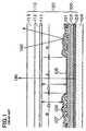
- A liquid crystal display device comprising:the first substrate (20) being comprised of:(a) a first substrate (20);(b) a second substrate (40) spaced away from and facing the first substrate (20); and(c) a liquid crystal layer (50) sandwiched between the first and second substrates (20, 40),the second substrate (40) being comprised of:(a1) a first transparent substrate (21) having a first area (A) through which a light is allowed to pass and a second area (B) in which a light is reflected;(a2) first to N-th 1st retardation plates (27, 28) arranged on the first transparent substrate (21) at the opposite side of the liquid crystal layer (50) wherein a K-th 1st retardation plate (27) is closer to the first transparent substrate (21) than a (K+1)-th 1st retardation plate (28), and wherein N is an integer equal to or greater than 1, and K is an integer equal to or greater than 1; and(a3) a first polarizer (29) arranged on the N-th 1st retardation plate (28),characterized in that(b1) a second transparent substrate (41);(b2) first to N-th 2nd retardation plates (42, 43) arranged on the second transparent substrate (41) at the opposite side of the liquid crystal layer (50) wherein a K-th 2nd retardation plate (42) is closer to the second transparent substrate (41) than a (K+1)-th 2nd retardation plate (43), and wherein N is an integer equal to or greater than 1, and K is an integer equal to or greater than 1; and(b3) a second polarizer (44) arranged on the N-th 2nd retardation plate (43),
assuming that a retardation plate among the first to N-th 1st retardation plates (27, 28) has an optical axis arranged at a first angle relative to a reference direction and a retardation plate among the first to N-th 2nd retardation plates (42, 43), corresponding to the retardation plate among the first to N-th 1st retardation plates (27, 28), has an optical axis arranged at a second angle relative to the reference direction, the first and second angles are different from each other by about 90 degrees. - The liquid crystal display device as set forth in claim 1, wherein a retardation plate (27) arranged closest to the first transparent substrate (21) among the first to N-th 1st retardation plates (27, 28) has retardation in the range of 140 nm to 160 nm, and a retardation plate (43) arranged remotest from the second transparent substrate (41) among the first to N-th 2nd retardation plates (42, 43) has retardation in the range of 250 nm to 300 nm.
- The liquid crystal display device as set forth in claim 1 or 2, wherein a retardation plate (27) arranged closest to the first transparent substrate (21) among the first to N-th 1st retardation plates (27, 28) is arranged at an angle in the range of 90 to 120 degrees relative to a reference direction, a retardation plate (28) arranged remotest from the first transparent substrate (21) among the first to N-th 1st retardation plates (27, 28) is arranged at an angle in the range of 150 to 180 degrees relative to the reference direction, and the first polarizer (29) is arranged at an angle in the range of -15 to 15 degrees relative to the reference direction,
and wherein a retardation plate (42) arranged closest to the second transparent substrate (41) among the first to N-th 2nd retardation plates (42, 43) is arranged at an angle in the range of 60 to 90 degrees relative to the reference direction, a retardation plate (43) arranged remotest from the second transparent substrate (41) among the first to N-th 2nd retardation plates (42, 43) is arranged at an angle in the range of 60 to 90 degrees relative to the reference direction, and the second polarizer (44) is arranged at an angle in the range of 75 to 105 degrees relative to the reference direction. - The liquid crystal display device as set forth in claim 1 or 2, wherein a retardation plate (27) arranged closest to the first transparent substrate (21) among the first to N-th 1st retardation plates (27, 28) is arranged at an angle in the range of -20 to 10 degrees relative to a reference direction, a retardation plate (28) arranged remotest from the first transparent substrate (21) among the first to N-th 1st retardation plates (27, 28) is arranged at an angle in the range of 95 to 125 degrees relative to the reference direction, and the first polarizer (29) is arranged at an angle in the range of -15 to 15 degrees relative to the reference direction,
and wherein a retardation plate (42) arranged closest to the second transparent substrate (41) among the first to N-th 2nd retardation plates (42, 43) is arranged at an angle in the range of 0 to 30 degrees relative to the reference direction, a retardation plate (43) arranged remotest from the second transparent substrate (41) among the first to N-th 2nd retardation plates (42, 43) is arranged at an angle in the range of 60 to 90 degrees relative to the reference direction, and the second polarizer (44) is arranged at an angle in the range of 75 to 105 degrees relative to the reference direction. - The liquid crystal display device as set forth in claim 1 or 2, wherein a retardation plate (27) arranged closest to the first transparent substrate (21) among the first to N-th 1st retardation plates (27, 28) is arranged at an angle in the range of 75 to 105 degrees relative to a reference direction, a retardation plate (28) arranged remotest from the first transparent substrate (21) among the first to N-th 1st retardation plates (27, 28) is arranged at an angle in the range of 135 to 165 degrees relative to the reference direction, and the first polarizer (29) is arranged at an angle in the range of 150 to 180 degrees relative to the reference direction,
and wherein a retardation plate (42) arranged closest to the second transparent substrate (41) among the first to N-th 2nd retardation plates (42, 43) is arranged at an angle in the range of -15 to 15 degrees relative to the reference direction, a retardation plate (43) arranged remotest from the second transparent substrate (41) among the first to N-th 2nd retardation plates (42, 43) is arranged at an angle in the range of 45 to 75 degrees relative to the reference direction, and the second polarizer (44) is arranged at an angle in the range of 60 to 90 degrees relative to the reference direction. - The liquid crystal display device as set forth in claim 1, wherein a thickness of the liquid crystal layer (50) in the first area (A) is almost equal to a thickness of the liquid crystal layer (50) in the second area (B).
- The liquid crystal display device as set forth in claim 1, wherein a thickness of the liquid crystal layer (50) in the first area (A) is smaller than a thickness of the liquid crystal layer (50) in the second area (B).
- The liquid crystal display device as set forth in claim 1, wherein a retardation plate (27) arranged closest to the first transparent substrate (21) among the first to N-th 1st retardation plates (27, 28) has retardation in the range of 125 nm to 155 nm, a retardation plate (42) arranged remotest from the second transparent substrate (41) among the first to N-th 2nd retardation plates (42, 43) has retardation in the range of 250 nm to 300 nm, and a retardation plate (42) arranged closet to the second transparent substrate (41) among the first to N-th 2nd retardation plates (42, 43) has retardation in the range of 140 nm to 170 nm,
- The liquid crystal display device as set forth in claim 8, wherein a thickness of the liquid crystal layer (50) in the first area (A) is almost equal to a thickness of the liquid crystal layer (50) in the second area (B).
- The liquid crystal display device as set forth in claim 8, wherein a thickness of the liquid crystal layer (50) in the first area (A) is smaller than a thickness of the liquid crystal layer (50) in the second area (B).
- A liquid crystal display device comprising:wherein the first transparent substrate (20) has a first area (A) through which a light is allowed to pass and a second area (B) in which a light is reflected,(a) a first transparent substrate (20);(b) a second substrate (40) spaced away from and facing the first transparent substrate (20); and(c) a liquid crystal layer (50) sandwiched between the first transparent substrate (20) and the second substrate (40),
characterized in that
a reflection electrode (25) is formed in the second area (B), the reflection electrode (25) being comprised of an underlying film (25a) formed on an electrically insulating film (24) and composed of one of molybdenum, chromium, titanium and tantalum, and an overlying film (25b) formed on the underlying film (25a) and composed of one of aluminum and silver,
a transmission electrode (26) is formed on the electrically insulating film (24) in the first area (A),
the reflection electrode (25) partially overlaps the transmission electrode (26) at their ends such that the reflection electrode (25) is located on the transmission electrode (26). - The liquid crystal display device as set forth in claim 11, wherein the electrically insulating film (24) is an organic film, the underlying film (25a) has a thickness in the range of 100 to 3000 angstroms, and the overlying film (25b) has a thickness in the range of 500 to 5000 angstroms.
- The liquid crystal display device as set forth in claim 11 or 12, wherein there is a first portion where the transmission electrode (26) overlaps the underlying film (25a), but does not overlap the overlying film (25b) between a second portion where the transmission electrode (26) overlaps the reflection electrode (25) and a third portion the transmission electrode (26) does not overlap the underlying film (25a), in a top view of a portion at which the transmission electrode (26) connects to the reflection electrode (25).
- The liquid crystal display device as set forth in claim 11, wherein the electrically insulating film (24) formed in the second area (B) is formed at a surface thereof with raised and recessed portions.
- The liquid crystal display device as set forth in claim 11, wherein the electrically insulating film (24) formed in first area (A) has a planarized surface.
- The liquid crystal display device as set forth in claim 13, wherein the second portion is in a tapered form, and the first portion has a thickness equal to or greater than 0.5 micrometers.
- The liquid crystal display device as set forth in claim 11, wherein a thickness of the liquid crystal layer (50) in the first area (A) is almost equal to a thickness of the liquid crystal layer (50) in the second area (B).
- The liquid crystal display device as set forth in claim 11, wherein a thickness of the liquid crystal layer (50) in the first area (A) is smaller than a thickness of the liquid crystal layer (50) in the second area (B).
- An electronic device including a liquid crystal display device defined in any one of claims 1 to 18.
- A method of fabricating a liquid crystal display device comprising:the method comprising the steps of:(a) a first transparent substrate (20) having a first area (A) through which a light is allowed to pass and a second area (B) in which a light is reflected;(b) a second substrate (40) spaced away from and facing the first transparent substrate (20); and(c) a liquid crystal layer (50) sandwiched between the first transparent substrate (20) and the second substrate (40),the transparent electrode (26) being electrically connected to the overlying film (25b) through the underlying film (25a).(a) forming an electrically insulating film (24) which has raised and recessed portions at a surface in the second area (B), and has a planarized surface in the first area (A);(b) forming a transparent electrode (26) on the electrically insulating film (24) in the first area (A);(c) forming an underlying film (25a) and an overlying, film (25b) entirely over the first transparent substrate (20), the overlying film (25b) being composed of aluminum or silver; and(d) patterning the both underlying and overlying films (25a, 25b),
Priority Applications (1)
| Application Number | Priority Date | Filing Date | Title |
|---|---|---|---|
| EP03021318A EP1376206B1 (en) | 2001-04-27 | 2002-04-25 | Liquid crystal display device |
Applications Claiming Priority (2)
| Application Number | Priority Date | Filing Date | Title |
|---|---|---|---|
| JP2001132744A JP5131505B2 (en) | 2001-04-27 | 2001-04-27 | Liquid crystal display |
| JP2001132744 | 2001-04-27 |
Related Child Applications (1)
| Application Number | Title | Priority Date | Filing Date |
|---|---|---|---|
| EP03021318A Division EP1376206B1 (en) | 2001-04-27 | 2002-04-25 | Liquid crystal display device |
Publications (3)
| Publication Number | Publication Date |
|---|---|
| EP1255154A2 true EP1255154A2 (en) | 2002-11-06 |
| EP1255154A3 EP1255154A3 (en) | 2002-12-04 |
| EP1255154B1 EP1255154B1 (en) | 2007-04-11 |
Family
ID=18980711
Family Applications (2)
| Application Number | Title | Priority Date | Filing Date |
|---|---|---|---|
| EP03021318A Expired - Lifetime EP1376206B1 (en) | 2001-04-27 | 2002-04-25 | Liquid crystal display device |
| EP02009485A Expired - Lifetime EP1255154B1 (en) | 2001-04-27 | 2002-04-25 | Liquid crystal display device |
Family Applications Before (1)
| Application Number | Title | Priority Date | Filing Date |
|---|---|---|---|
| EP03021318A Expired - Lifetime EP1376206B1 (en) | 2001-04-27 | 2002-04-25 | Liquid crystal display device |
Country Status (6)
| Country | Link |
|---|---|
| US (2) | US7894028B2 (en) |
| EP (2) | EP1376206B1 (en) |
| JP (1) | JP5131505B2 (en) |
| KR (1) | KR100474367B1 (en) |
| DE (2) | DE60219451T2 (en) |
| TW (1) | TW583459B (en) |
Cited By (2)
| Publication number | Priority date | Publication date | Assignee | Title |
|---|---|---|---|---|
| EP1284433A3 (en) * | 2001-08-06 | 2003-03-19 | Nec Corporation | Transflective liquid crystal display and method for manufacturing the same |
| WO2003054621A1 (en) * | 2001-12-11 | 2003-07-03 | Sony Corporation | Liquid crystal display apparatus |
Families Citing this family (11)
| Publication number | Priority date | Publication date | Assignee | Title |
|---|---|---|---|---|
| TWI226965B (en) * | 2001-10-30 | 2005-01-21 | Nec Lcd Technologies Ltd | Semi-transmission type liquid crystal display and fabrication method thereof |
| KR20040006555A (en) * | 2002-07-12 | 2004-01-24 | 삼성전자주식회사 | Liquid crystal display |
| KR100915235B1 (en) * | 2002-12-23 | 2009-09-02 | 삼성전자주식회사 | Transmissive and reflective type liquid crystal display |
| TW200512493A (en) * | 2003-07-31 | 2005-04-01 | Samsung Electronics Co Ltd | Optical sheet assembly and liquid crystal display apparatus having the same |
| US8023073B2 (en) | 2006-01-26 | 2011-09-20 | Samsung Electronics Co., Ltd. | Color filter display panel, thin film transistor array panel, liquid crystal display thereof, and method thereof |
| JP4638462B2 (en) | 2007-03-26 | 2011-02-23 | 株式会社 日立ディスプレイズ | Liquid crystal display device |
| TWI373664B (en) * | 2008-05-15 | 2012-10-01 | Benq Materials Corp | Flat display device |
| TWI500163B (en) * | 2012-10-15 | 2015-09-11 | Innocom Tech Shenzhen Co Ltd | Low temperature poly-silicon thin film transistor, manufacturing method thereof, and display device |
| US9651426B2 (en) * | 2015-06-30 | 2017-05-16 | Agilent Technologies, Inc. | Light source with controllable linear polarization |
| US10184835B2 (en) * | 2015-09-23 | 2019-01-22 | Agilent Technologies, Inc. | High dynamic range infrared imaging spectroscopy |
| CN111613629B (en) * | 2020-06-28 | 2022-09-09 | 武汉华星光电技术有限公司 | Conductive film layer, preparation method of conductive film layer and display device |
Citations (5)
| Publication number | Priority date | Publication date | Assignee | Title |
|---|---|---|---|---|
| JPH11101992A (en) * | 1997-07-28 | 1999-04-13 | Sharp Corp | Liquid crystal display device |
| JP2000035570A (en) * | 1998-07-16 | 2000-02-02 | Sharp Corp | Liquid crystal display device |
| WO2000075718A1 (en) * | 1999-06-07 | 2000-12-14 | Citizen Watch Co., Ltd. | Liquid crystal display |
| EP1072926A1 (en) * | 1999-02-15 | 2001-01-31 | Citizen Watch Co., Ltd. | Liquid-crystal display |
| US6195140B1 (en) * | 1997-07-28 | 2001-02-27 | Sharp Kabushiki Kaisha | Liquid crystal display in which at least one pixel includes both a transmissive region and a reflective region |
Family Cites Families (16)
| Publication number | Priority date | Publication date | Assignee | Title |
|---|---|---|---|---|
| US5657140A (en) * | 1993-12-15 | 1997-08-12 | Ois Optical Imaging Systems, Inc. | Normally white twisted nematic LCD with positive and negative retarders |
| US6141070A (en) * | 1997-06-13 | 2000-10-31 | Citizen Watch Co., Ltd. | Normally black liquid crystal display with twisted compensator and . .DELTAnd of 1500-1800 nm |
| US6295109B1 (en) * | 1997-12-26 | 2001-09-25 | Sharp Kabushiki Kaisha | LCD with plurality of pixels having reflective and transmissive regions |
| KR100471012B1 (en) * | 1998-02-04 | 2005-03-07 | 세이코 엡슨 가부시키가이샤 | Liquid crystal display and electronic device |
| JP3410656B2 (en) * | 1998-03-31 | 2003-05-26 | シャープ株式会社 | Liquid crystal display device and manufacturing method thereof |
| JPH11311780A (en) | 1998-04-27 | 1999-11-09 | Kawaguchiko Seimitsu Kk | Liquid crystal display device |
| JP3544629B2 (en) | 1999-03-10 | 2004-07-21 | シャープ株式会社 | Liquid crystal display |
| JP2000275660A (en) * | 1999-03-24 | 2000-10-06 | Sharp Corp | Liquid crystal display device and its production |
| KR100394987B1 (en) * | 2000-04-07 | 2003-08-19 | 엘지.필립스 엘시디 주식회사 | transflective liquid crystal display device |
| KR100367280B1 (en) * | 2000-05-08 | 2003-01-09 | 엘지.필립스 엘시디 주식회사 | Method for fabricating transflective LCD |
| JP3763401B2 (en) * | 2000-05-31 | 2006-04-05 | シャープ株式会社 | Liquid crystal display |
| JP2002098954A (en) * | 2000-07-21 | 2002-04-05 | Citizen Watch Co Ltd | Translucent reflective liquid crystal display device |
| US6620655B2 (en) * | 2000-11-01 | 2003-09-16 | Lg.Phillips Lcd Co., Ltd. | Array substrate for transflective LCD device and method of fabricating the same |
| JP2003066441A (en) * | 2001-08-30 | 2003-03-05 | Rohm Co Ltd | Liquid crystal display element provided with reflection sheet and method for manufacturing the sheet |
| US6919946B2 (en) * | 2002-04-16 | 2005-07-19 | 3M Innovative Properties Company | Compensators for liquid crystal displays and the use and manufacture of the compensators |
| JP4480599B2 (en) * | 2005-02-14 | 2010-06-16 | Nec液晶テクノロジー株式会社 | Reflector, method for manufacturing the same, and liquid crystal display device |
-
2001
- 2001-04-27 JP JP2001132744A patent/JP5131505B2/en not_active Expired - Lifetime
-
2002
- 2002-04-25 EP EP03021318A patent/EP1376206B1/en not_active Expired - Lifetime
- 2002-04-25 EP EP02009485A patent/EP1255154B1/en not_active Expired - Lifetime
- 2002-04-25 DE DE60219451T patent/DE60219451T2/en not_active Expired - Lifetime
- 2002-04-25 DE DE60219386T patent/DE60219386T2/en not_active Expired - Lifetime
- 2002-04-26 US US10/132,828 patent/US7894028B2/en not_active Expired - Fee Related
- 2002-04-26 TW TW091108818A patent/TW583459B/en active
- 2002-04-26 KR KR10-2002-0023161A patent/KR100474367B1/en not_active IP Right Cessation
-
2011
- 2011-02-03 US US13/020,309 patent/US8755011B2/en not_active Expired - Lifetime
Patent Citations (5)
| Publication number | Priority date | Publication date | Assignee | Title |
|---|---|---|---|---|
| JPH11101992A (en) * | 1997-07-28 | 1999-04-13 | Sharp Corp | Liquid crystal display device |
| US6195140B1 (en) * | 1997-07-28 | 2001-02-27 | Sharp Kabushiki Kaisha | Liquid crystal display in which at least one pixel includes both a transmissive region and a reflective region |
| JP2000035570A (en) * | 1998-07-16 | 2000-02-02 | Sharp Corp | Liquid crystal display device |
| EP1072926A1 (en) * | 1999-02-15 | 2001-01-31 | Citizen Watch Co., Ltd. | Liquid-crystal display |
| WO2000075718A1 (en) * | 1999-06-07 | 2000-12-14 | Citizen Watch Co., Ltd. | Liquid crystal display |
Non-Patent Citations (2)
| Title |
|---|
| PATENT ABSTRACTS OF JAPAN vol. 1999, no. 09, 30 July 1999 (1999-07-30) -& JP 11 101992 A (SHARP CORP), 13 April 1999 (1999-04-13) * |
| PATENT ABSTRACTS OF JAPAN vol. 2000, no. 05, 14 September 2000 (2000-09-14) -& JP 2000 035570 A (SHARP CORP), 2 February 2000 (2000-02-02) -& US 2001/055082 A1 (KUBO ET AL) 27 December 2001 (2001-12-27) * |
Cited By (5)
| Publication number | Priority date | Publication date | Assignee | Title |
|---|---|---|---|---|
| EP1284433A3 (en) * | 2001-08-06 | 2003-03-19 | Nec Corporation | Transflective liquid crystal display and method for manufacturing the same |
| US6853421B2 (en) | 2001-08-06 | 2005-02-08 | Nec Corporation | Transflective type LCD and method for manufacturing the same |
| US7817229B2 (en) | 2001-08-06 | 2010-10-19 | Nec Lcd Technologies, Ltd. | Transflective type LCD and method for manufacturing the same |
| US7990501B2 (en) | 2001-08-06 | 2011-08-02 | Nec Lcd Technologies, Ltd. | Transflective type LCD and method for manufacturing the same |
| WO2003054621A1 (en) * | 2001-12-11 | 2003-07-03 | Sony Corporation | Liquid crystal display apparatus |
Also Published As
| Publication number | Publication date |
|---|---|
| KR20020083506A (en) | 2002-11-02 |
| US8755011B2 (en) | 2014-06-17 |
| KR100474367B1 (en) | 2005-03-08 |
| US20110128484A1 (en) | 2011-06-02 |
| EP1255154A3 (en) | 2002-12-04 |
| JP5131505B2 (en) | 2013-01-30 |
| EP1376206B1 (en) | 2007-04-11 |
| US20020159011A1 (en) | 2002-10-31 |
| TW583459B (en) | 2004-04-11 |
| DE60219451D1 (en) | 2007-05-24 |
| US7894028B2 (en) | 2011-02-22 |
| DE60219386T2 (en) | 2007-12-20 |
| JP2002328370A (en) | 2002-11-15 |
| EP1376206A1 (en) | 2004-01-02 |
| EP1255154B1 (en) | 2007-04-11 |
| DE60219451T2 (en) | 2007-12-20 |
| DE60219386D1 (en) | 2007-05-24 |
Similar Documents
| Publication | Publication Date | Title |
|---|---|---|
| US8755011B2 (en) | Liquid crystal display device and method of fabricating the same | |
| US6680765B1 (en) | Liquid crystal device and electronic apparatus | |
| US6885420B2 (en) | Array panel for a transflective liquid crystal display device | |
| US6717632B2 (en) | Transflective liquid crystal display device and manufacturing method thereof | |
| US6636286B1 (en) | Transflective liquid crystal display device having reflective and transparent pixel electrodes | |
| US20040169810A1 (en) | Liquid crystal display and manufacturing method thereof | |
| US20040233357A1 (en) | Liquid crystal display device | |
| JP2000019563A (en) | Liquid crystal display device | |
| JPH11242226A (en) | Liquid crystal display device | |
| US20030160920A1 (en) | Transflective liquid crystal display device and method of manufacturing the same | |
| US20060125984A1 (en) | Display device and thin film transistor array panel for display device and manufacturing method thereof | |
| US6661485B2 (en) | Reflective liquid crystal display device using a cholesteric liquid crystal color filter | |
| US20010022638A1 (en) | Transflective liquid crystal display device | |
| US7012662B2 (en) | Transflective LCD with twist angle less than 90 degrees and 4 compensation films | |
| JP3283221B2 (en) | Liquid crystal display device | |
| US8120734B2 (en) | Transflective liquid crystal display and fabrication method thereof | |
| JP2006184363A (en) | Liquid crystal display device | |
| JPH10142621A (en) | Reflection type liquid crystal display device | |
| JP2002372710A (en) | Liquid crystal display device | |
| JP5152279B2 (en) | Liquid crystal display | |
| JP5594479B2 (en) | Liquid crystal display | |
| JP2002333624A (en) | Liquid crystal display device | |
| KR20020017048A (en) | Reflective and Transflective Liquid Crystal Display Device | |
| KR20110076367A (en) | In-plane switching mode transflective type liquid crystal display device |
Legal Events
| Date | Code | Title | Description |
|---|---|---|---|
| PUAI | Public reference made under article 153(3) epc to a published international application that has entered the european phase |
Free format text: ORIGINAL CODE: 0009012 |
|
| PUAL | Search report despatched |
Free format text: ORIGINAL CODE: 0009013 |
|
| AK | Designated contracting states |
Kind code of ref document: A2 Designated state(s): AT BE CH CY DE DK ES FI FR GB GR IE IT LI LU MC NL PT SE TR |
|
| AX | Request for extension of the european patent |
Free format text: AL;LT;LV;MK;RO;SI |
|
| AK | Designated contracting states |
Kind code of ref document: A3 Designated state(s): AT BE CH CY DE DK ES FI FR GB GR IE IT LI LU MC NL PT SE TR |
|
| AX | Request for extension of the european patent |
Free format text: AL;LT;LV;MK;RO;SI |
|
| 17P | Request for examination filed |
Effective date: 20021024 |
|
| 17Q | First examination report despatched |
Effective date: 20030124 |
|
| RAP1 | Party data changed (applicant data changed or rights of an application transferred) |
Owner name: NEC LCD TECHNOLOGIES, LTD. Owner name: NEC CORPORATION |
|
| AKX | Designation fees paid |
Designated state(s): DE FI FR SE |
|
| GRAP | Despatch of communication of intention to grant a patent |
Free format text: ORIGINAL CODE: EPIDOSNIGR1 |
|
| RTI1 | Title (correction) |
Free format text: LIQUID CRYSTAL DISPLAY DEVICE |
|
| GRAS | Grant fee paid |
Free format text: ORIGINAL CODE: EPIDOSNIGR3 |
|
| GRAA | (expected) grant |
Free format text: ORIGINAL CODE: 0009210 |
|
| AK | Designated contracting states |
Kind code of ref document: B1 Designated state(s): DE FI FR SE |
|
| REF | Corresponds to: |
Ref document number: 60219386 Country of ref document: DE Date of ref document: 20070524 Kind code of ref document: P |
|
| REG | Reference to a national code |
Ref country code: SE Ref legal event code: TRGR |
|
| ET | Fr: translation filed | ||
| PLBE | No opposition filed within time limit |
Free format text: ORIGINAL CODE: 0009261 |
|
| STAA | Information on the status of an ep patent application or granted ep patent |
Free format text: STATUS: NO OPPOSITION FILED WITHIN TIME LIMIT |
|
| 26N | No opposition filed |
Effective date: 20080114 |
|
| REG | Reference to a national code |
Ref country code: FR Ref legal event code: TP |
|
| REG | Reference to a national code |
Ref country code: DE Ref legal event code: R082 Ref document number: 60219386 Country of ref document: DE Representative=s name: GLAWE DELFS MOLL PARTNERSCHAFT MBB VON PATENT-, DE Effective date: 20110919 Ref country code: DE Ref legal event code: R081 Ref document number: 60219386 Country of ref document: DE Owner name: NLT TECHNOLOGIES, LTD., JP Free format text: FORMER OWNER: NEC LCD TECHNOLOGIES, LTD., KAWASAKI, JP Effective date: 20110919 Ref country code: DE Ref legal event code: R081 Ref document number: 60219386 Country of ref document: DE Owner name: NLT TECHNOLOGIES, LTD., KAWASAKI, JP Free format text: FORMER OWNER: NEC LCD TECHNOLOGIES, LTD., KAWASAKI, KANAGAWA, JP Effective date: 20110919 |
|
| REG | Reference to a national code |
Ref country code: FR Ref legal event code: CA Effective date: 20111013 Ref country code: FR Ref legal event code: CD Owner name: NLT TECHNOLOGIES, LTD, JP Effective date: 20111013 |
|
| REG | Reference to a national code |
Ref country code: FR Ref legal event code: PLFP Year of fee payment: 15 |
|
| PGFP | Annual fee paid to national office [announced via postgrant information from national office to epo] |
Ref country code: FI Payment date: 20160411 Year of fee payment: 15 |
|
| PGFP | Annual fee paid to national office [announced via postgrant information from national office to epo] |
Ref country code: SE Payment date: 20160412 Year of fee payment: 15 |
|
| REG | Reference to a national code |
Ref country code: FR Ref legal event code: PLFP Year of fee payment: 16 |
|
| PG25 | Lapsed in a contracting state [announced via postgrant information from national office to epo] |
Ref country code: FI Free format text: LAPSE BECAUSE OF NON-PAYMENT OF DUE FEES Effective date: 20170425 |
|
| PG25 | Lapsed in a contracting state [announced via postgrant information from national office to epo] |
Ref country code: SE Free format text: LAPSE BECAUSE OF NON-PAYMENT OF DUE FEES Effective date: 20170426 |
|
| REG | Reference to a national code |
Ref country code: FR Ref legal event code: PLFP Year of fee payment: 17 |
|
| PGFP | Annual fee paid to national office [announced via postgrant information from national office to epo] |
Ref country code: FR Payment date: 20210423 Year of fee payment: 20 Ref country code: DE Payment date: 20210420 Year of fee payment: 20 |
|
| REG | Reference to a national code |
Ref country code: DE Ref legal event code: R071 Ref document number: 60219386 Country of ref document: DE |