EP1248297A2 - Inductance element and semiconductor device - Google Patents
Inductance element and semiconductor device Download PDFInfo
- Publication number
- EP1248297A2 EP1248297A2 EP02251762A EP02251762A EP1248297A2 EP 1248297 A2 EP1248297 A2 EP 1248297A2 EP 02251762 A EP02251762 A EP 02251762A EP 02251762 A EP02251762 A EP 02251762A EP 1248297 A2 EP1248297 A2 EP 1248297A2
- Authority
- EP
- European Patent Office
- Prior art keywords
- conductive film
- film pattern
- inductance element
- semiconductor substrate
- inductance
- Prior art date
- Legal status (The legal status is an assumption and is not a legal conclusion. Google has not performed a legal analysis and makes no representation as to the accuracy of the status listed.)
- Granted
Links
Images



Classifications
-
- H—ELECTRICITY
- H10—SEMICONDUCTOR DEVICES; ELECTRIC SOLID-STATE DEVICES NOT OTHERWISE PROVIDED FOR
- H10D—INORGANIC ELECTRIC SEMICONDUCTOR DEVICES
- H10D1/00—Resistors, capacitors or inductors
- H10D1/20—Inductors
-
- H—ELECTRICITY
- H01—ELECTRIC ELEMENTS
- H01F—MAGNETS; INDUCTANCES; TRANSFORMERS; SELECTION OF MATERIALS FOR THEIR MAGNETIC PROPERTIES
- H01F17/00—Fixed inductances of the signal type
- H01F17/0006—Printed inductances
-
- H—ELECTRICITY
- H10—SEMICONDUCTOR DEVICES; ELECTRIC SOLID-STATE DEVICES NOT OTHERWISE PROVIDED FOR
- H10D—INORGANIC ELECTRIC SEMICONDUCTOR DEVICES
- H10D84/00—Integrated devices formed in or on semiconductor substrates that comprise only semiconducting layers, e.g. on Si wafers or on GaAs-on-Si wafers
-
- H—ELECTRICITY
- H10—SEMICONDUCTOR DEVICES; ELECTRIC SOLID-STATE DEVICES NOT OTHERWISE PROVIDED FOR
- H10W—GENERIC PACKAGES, INTERCONNECTIONS, CONNECTORS OR OTHER CONSTRUCTIONAL DETAILS OF DEVICES COVERED BY CLASS H10
- H10W20/00—Interconnections in chips, wafers or substrates
- H10W20/40—Interconnections external to wafers or substrates, e.g. back-end-of-line [BEOL] metallisations or vias connecting to gate electrodes
- H10W20/497—Inductive arrangements or effects of, or between, wiring layers
-
- H—ELECTRICITY
- H01—ELECTRIC ELEMENTS
- H01F—MAGNETS; INDUCTANCES; TRANSFORMERS; SELECTION OF MATERIALS FOR THEIR MAGNETIC PROPERTIES
- H01F17/00—Fixed inductances of the signal type
- H01F17/0006—Printed inductances
- H01F2017/0046—Printed inductances with a conductive path having a bridge
-
- H—ELECTRICITY
- H01—ELECTRIC ELEMENTS
- H01F—MAGNETS; INDUCTANCES; TRANSFORMERS; SELECTION OF MATERIALS FOR THEIR MAGNETIC PROPERTIES
- H01F27/00—Details of transformers or inductances, in general
- H01F27/34—Special means for preventing or reducing unwanted electric or magnetic effects, e.g. no-load losses, reactive currents, harmonics, oscillations, leakage fields
Definitions
- the present invention relates to an inductance element and a semiconductor device which includes the inductance element therein, and particularly to a structure of an inductance element which reduces signal loss brought about therein.
- an inductance element is required in the high frequency integrated circuit.
- passive elements such as a transistor, a resistor, and a capacitor
- an inductance element is required in the high frequency integrated circuit.
- all the foregoing passive elements including the inductance element need to be provided on the silicon semiconductor substrate.
- the inductance element for a silicon IC is typically provided on the silicon semiconductor substrate via an insulating film, and is made, for example, by providing a belt-shaped conductive film of aluminum (Al) in a spiral manner (in a vortex manner) or in a meandering manner.
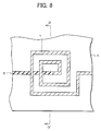
- FIG. 8 is a plan view which schematically shows a structure of an inductance element formation section in the conventional semiconductor device.
- FIG. 9 is a cross sectional view in a line D-D' of the inductance formation section of the semiconductor device shown in FIG. 8. Note that, in FIG. 8, insulating films 5, 6, and 7 are not displayed, but patterns are given to respective components. That is, the same component has the same pattern in FIG. 8.
- the conventional inductance element has the following structure.
- the insulating films 5 and 6 are provided on a main surface of a semiconductor substrate 4, such as a silicon semiconductor substrate, in this order.
- a connection wire 3 connected to one terminal of an inductance section which is composed of a conductive film pattern 1 described later, is provided on the insulating film 6.
- the inductance section which is composed of the conductive film pattern 1 provided in a spiral manner (in a vortex manner) as shown in FIG. 8, is provided on the insulating film 7 which covers the connection wire 3.
- the one terminal (drawing terminal) is formed at a substantially central portion of the spiral. Further, the inductance section is connected to the connection wire 3 via a via-hole (not shown) at a position of the terminal, that is, at a substantially central portion of the spiral.
- the connection wire 3 is externally drawn from the inductance section as a drawing wire for connecting to an external portion of the inductance element.
- the inductance element is, for example, provided in a semiconductor device, that is, provided on a semiconductor substrate of the semiconductor device internally or externally.
- the foregoing semiconductor substrate 4 is used as the semiconductor substrate of the semiconductor device, so that the inductance element is electrically connected to an electrode pad (not shown) etc, provided on the main surface of the semiconductor substrate 4, which is electrically connected to a transistor (not shown) etc. making up an integrated circuit such as an LSI.
- the inductance element is used at a high frequency band.
- the signal loss of the semiconductor substrate 4 occurs frequently particularly at a high frequency band.
- the performance of the inductance element is deteriorated by a parasitic component which occurs due to a shape etc. of the conductive film pattern 1 making up the inductance section.
- a signal loss at an area under the spiral conductive film pattern 1 is extremely large, so that the inductance element cannot be preferably used at a high frequency band.
- Japanese Unexamined Patent Publication No. 181289/1994 discloses an inductance element having the following structure.
- a grounded metallic thin film is provided near the conductive film pattern 1 formed above the semiconductor substrate 4, so that characteristic impedance is adjusted. Thus, reflection and loss of a high frequency signal are reduced.
- the influence upon the semiconductor substrate 4, which is exerted by electromagnetic induction of a current applied to the inductance section, is reduced by forming an inductance section on a grounded metallic thin film, so that a signal loss of the semiconductor substrate 4, that is, a characteristic loss is reduced.
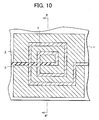
- FIG. 10 is a plan view showing a schematic structure of an inductance element formation section of the semiconductor device recited in Japanese Unexamined Patent Publication No. 181289/1994.
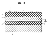
- FIG. 11 is a cross sectional view in a line E-E' of the semiconductor device shown in FIG. 10. Note that, in FIG. 10, for the sake of convenience in description, the insulating films 5, 6, and 7 shown in FIG. 11 are not displayed, and patterns are given to the respective components. That is, in FIG. 10, the same pattern is given to the same component. Further, in the following description, the same signs are given to components having the same functions as components shown in FIG. 8 and FIG. 9, and description thereof is omitted.
- the insulating film 5 is provided as a first insulating film on a main surface of the semiconductor substrate 4, and a metallic thin film 2, which is a grounding metallic film (grounding potential layer), is provided on the insulating film 5 so that substantially all the surface of the semiconductor substrate 4 except for marginal portions is covered. Further, in the semiconductor device, after the metallic thin film 2 is coated by the insulating film 6 which serves as a second insulating film, the connection wire 3 which serves as a drawing wire for external connection at the inductance section is provided on the insulating film 6.
- the insulating film 7 which serves as a third insulating film is provided so as to cover the connection wire 3, and the conductive film pattern 1 making up the inductance section is provided in a spiral manner (in a vortex manner) on the insulating film 7.
- the grounded metallic thin film 2 is provided on the insulating film 5 formed on the main surface of the semiconductor substrate 4, so that parasitic capacitance is formed at a portion where the conductive film pattern 1 or the connection wire 3 is lapped by the metallic thin film 2 in a laminating direction above the semiconductor substrate 4. That is, between the conductive film pattern 1 and the grounded metallic thin film 2, and between the connection wire 3 used as a drawing wire of the conductive film pattern 1 and the metallic thin film 2, the parasitic capacitance is formed.
- the inductance element compared with an inductance element shown in FIG. 8 and FIG.
- the parasitic capacitance which occurs between the conductive film pattern 1 making up the inductance section and the metallic thin film 2, causes a characteristic of the inductance element, furthermore, a characteristic of the semiconductor device having the inductance element therein to deteriorate.
- the object of the present invention is to provide an inductance element and a semiconductor device in which signal loss which occurs in a semiconductor substrate is restrained, and a parasitic capacitance is reduced compared with a conventional inductance element.
- the inductance element includes an inductance section, provided above a semiconductor substrate via insulating films, which is composed of a first conductive film pattern setted to have a predetermined inductance value, wherein an impurity region, which has a grounding potential and a denser impurity than that of the semiconductor substrate, is provided on the semiconductor substrate so as to be positioned at least at an area under the first conductive film pattern.
- the impurity region is provided on the semiconductor substrate so as to be positioned at least at the area under the first conductive film pattern, and the impurity region has the grounding potential and the denser impurity than that of the semiconductor substrate. Therefore, it is possible to provide the following high performance inductance element.
- the inductance element it is possible to reduce reflection and loss of a high frequency signal passing through the inductance section which result from electromagnetic induction of a current applied to the inductance section, so that it is possible to restrict decline of the Q value which indicates the performance of the inductance element with respect to frequency.
- the structure it is possible to enlarge a film thickness (distance) between the inductance section and a grounding surface, that is, a layer or an area which is used as the grounding potential layer, so that it is possible to reduce the parasitic capacitance, compared with the inductance element of Japanese Unexamined Patent Publication No. 181289/1994 (Tokukaihei 6-181289). Thus, it is possible to reduce attenuation of a signal level which is brought about by the parasitic capacitance.
- the semiconductor device according to the present invention includes the inductance element according to the present invention. It is preferable that the inductance element is provided in the semiconductor device.
- the inductance element is, for example, provided in the semiconductor device, so that it is possible to reduce reflection and loss of a high frequency signal passing through the inductance section which result from electromagnetic induction of a current applied to the inductance section, so that it is possible to restrict decline of the Q value which indicates the performance of the inductance element with respect to frequency.
- the parasitic capacitance can be reduced, so that it is possible to provide a semiconductor device having a high quality inductance characteristic.
- the inductance element is separated from a semiconductor substrate on which an integrated circuit making up the semiconductor device is provided, for example, the inductance element is separated from an integrated circuit formation section (element formation section) of the semiconductor substrate, so that it is possible to prevent other elements from being influenced by noise.
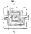
- FIG. 1 is a plan view showing a schematic structure of an inductance element of a semiconductor device according to the present embodiment.
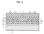
- FIG. 2 is a cross sectional view in a line A-A' of the semiconductor device shown in FIG. 1.
- each of FIG. 4 and FIG. 5 shows an example where the inductance element according to the present embodiment is connected to a circuit section of the semiconductor device, by a cross sectional view in a line B-B' of the semiconductor device shown in FIG. 1.
- insulating films 5, 6, and 7, shown in FIG. 2 are not displayed, and a pattern is given to each component. That is, in FIG. 1, the same pattern is given to the same component.
- the same signs are given to components having the same functions as components shown in BACKGROUND OF THE INVENTION, and description thereof is omitted.
- An inductance element according to the present embodiment is, for example, provided in a semiconductor device, that is, provided on a semiconductor substrate of the semiconductor device internally or externally.
- an inductance section which is composed of a conductive film pattern 1 (first conductive film pattern), is provided above a semiconductor substrate 4 via insulating films (insulating films 5, 6, and 7 in the present embodiment).
- the inductance element includes: a semiconductor substrate 4; an impurity region 9; an insulating film 5 (first insulating film); an insulating film 6 (second insulating film); an insulating film 7 (third insulating film); a conductive film 8 (second conductive film pattern); a connection wire 3 (third conductive film pattern); the conductive film pattern 1; a contact hole 10 (via-hole); and a via-hole 11 (see FIG. 4 and FIG. 5).
- the impurity region 9 is provided on a surface of the semiconductor substrate 4. Further, the insulating film 5 (first insulating film), the insulating film 6 (second insulating film), the insulating film 7 (third insulating film), the conductive film 8 (second conductive film pattern), and the connection wire 3 (third conductive film pattern) are provided above the semiconductor substrate 4. Further, the contact hole 10 (via-hole) electrically connects the conductive film 8 to the impurity region 9. The via-hole 11 electrically connects the connection wire 3 to the conductive film pattern 1.
- the inductance element that is, to form a semiconductor device by using the semiconductor substrate 4 having the inductance section, for example, it is possible to employ a process in which an integrated circuit such as an LSI is provided on the semiconductor substrate 4. Further, to form the semiconductor device, it is possible to employ a process in which the semiconductor substrate 4 having the inductance section is provided on a semiconductor substrate having the integrated circuit. Alternatively, to form the semiconductor device, it is possible to employ a process in which plural semiconductor substrates which includes the semiconductor substrate 4 having the inductance section are provided on a semiconductor substrate mounting section of a lead frame, so as to store the semiconductor substrates in a single package.
- the inductance element may be wired, and may be provided in a semiconductor substrate having a transistor etc. making up the LSI.
- the integrated circuit such as the LSI is provided on the semiconductor substrate 4 having the inductance section, and the inductance element is provided by using a wiring pattern, so that the number of parts is reduced and a manufacturing cost can be reduced.
- the impurity region 9 On a surface (main surface) of the semiconductor substrate 4 of the inductance element, the impurity region 9 whose impurity is denser than that of the semiconductor substrate 4 is provided, for example, so as to cover substantially all the surface (main surface) of the semiconductor substrate 4 of the inductance formation section, except for marginal portions of the semiconductor substrate 4.
- the impurity region 9, as shown in FIG. 1 and FIG. 2 is provided on the semiconductor substrate 4 so as to cover a whole area under an area where the conductive film pattern 1 is formed.
- a transistor etc. (not shown; for example, transistor 20 shown in FIG. 4), making up the integrated circuit such as the LSI, is provided.
- an electrode pad (connection electrode, grounding terminal; not shown), which is used to ground the conductive film 8 and to electrically connect the conductive film pattern 1 to the integrated circuit formed on the semiconductor substrate 4 so that the electrode pad is exposed.
- the electrode pad it is possible to use the transistor making up the integrated circuit such as the LSI so that, for example, the transistor is electrically connected to the electrode pad.
- a p type silicon semiconductor substrate is used as the semiconductor substrate 4, and a p type impurity region 9 having the same polarity as the semiconductor substrate 4 is provided on a surface (main surface) of the p type silicon semiconductor substrate.
- the impurity region 9 is used as a grounding region (grounding potential layer).
- the insulating film 5 is provided as the first insulating film so as to cover the impurity region 9.
- a grounded conductive film 8 which is used to ground the impurity region 9, is provided as the second conductive film pattern on the insulating film 5.
- the conductive film 8 is provided on the insulating film 5 so as not to be positioned under the conductive film pattern 1 making up the inductance section and under the connection wire 3 used as a drawing wire for connection of the inductance section, for example, the conductive film 8 is provided on an area except for areas under the conductive film pattern 1 and the connection wire 3.
- the conductive film 8 is provided so that the conductive film 8 is not lapped by the conductive film pattern 1, so that it is possible to enlarge the distance between the conductive film pattern 1 and a grounding surface (that is, grounding area (grounding potential layer)) opposite to the conductive film pattern 1. Therefore, it is possible to reduce the parasitic capacitance which occurs between the conductive film pattern 1 and the grounding area (grounding potential layer), or the impurity region 9 in the present embodiment.
- the conductive film 8 is provided so that the conductive film 8 is not lapped by the connection wire 3. As a result, it is possible to enlarge the distance between the connection wire 3 and the grounding surface (that is, grounding area (grounding potential layer)) opposite to the connection wire 3. Therefore, it is possible to reduce the parasitic capacitance which occurs between the connection wire 3 and the grounding area (grounding potential layer), or the impurity region 9 in the present embodiment.
- a contact hole 10 is provided under an area where the conductive film 8 is formed.
- the impurity region 9 is electrically connected to the conductive film 8 via the contact hole 10.
- the insulating film 6 is provided as the second insulating film so as to cover the conductive film 8.
- a drawing wire which is drawn to one terminal of the conductive film pattern 1 is provided, that is, the connection wire 3, consisting of a conductive film (conductive film pattern), which is used as a drawing wire of the inductance section, is provided.
- the conductive film pattern 1 is, as shown in FIG. 1, provided in a spiral (vortex) wiring pattern.
- the one terminal (drawing terminal) of the conductive film pattern 1 is formed at a substantially central portion of the spiral conductive film pattern 1.
- the spiral conductive film pattern 1 is connected to one end of the connection wire 3 via a via-hole 11 (for example, see FIG. 4) at the substantially central portion of the spiral.
- the other end of the connection wire 3 is connected to an electrode pad (not shown) which is exposed at the marginal portions of the main surface of the semiconductor substrate 4, or is connected to the transistor (for example, a transistor 20 shown in FIG. 4) etc. of the circuit section.
- connection wire 3 is used as a lead section for connecting the conductive film pattern 1 to the electrode pad provided on the marginal portions of the main surface of the semiconductor substrate 4, that is, the electrode pad connected to the integrated circuit etc. formed on the semiconductor substrate 4, or the transistor formed on the circuit section of the integrated circuit etc. Further, the conductive film pattern 1 is electrically connected from the central portion of the spiral to the outside, for example, to the integrated circuit formed on the semiconductor substrate 4, via the via-hole 11, by the connection wire 3. A current is applied to the conductive film pattern 1, so that the conductive film pattern 1 operates as an inductance element.
- a manufacturing method of the semiconductor device according to the present embodiment particularly, a manufacturing method of the inductance element (inductance element section) of the semiconductor device, are described as follows.
- the p type impurity region 9 is formed on the p type silicon semiconductor substrate used as the semiconductor substrate 4, in accordance with a method such as a low energy ion injection method in which, for example, boron trifluoride (BF3) typically used in a CMOS (complementary metal oxide semiconductor) process is used.
- a method such as a low energy ion injection method in which, for example, boron trifluoride (BF3) typically used in a CMOS (complementary metal oxide semiconductor) process is used.
- the insulating film 5 made of, for example, silicon dioxide (SiO 2 ) is formed by a known method such as plasma CVD (chemical vapor deposition).
- the contact holes 10 for connecting the impurity region 9 to the conductive film 8 are provided in predetermined areas of the insulating film 5 by using a photoresist, in accordance with RIE (Reactive Ion Etching) etc., and plating etc. is performed, so that the impurity region 9 is exposed partially.
- the conductive film 8 made of, for example, aluminum (Al) is formed so as to cover the contact holes 10 by using the photoresist, in accordance with methods such as deposition, sputtering, or printing.
- the contact hole 10 is connected to, for example, the electrode pad etc. which serves as a grounding point (grounding terminal) due to the conductive film 8, and is used as a contact hole for grounding the impurity region 9.
- the contact hole 10 and the conductive film 8 connected to the contact hole 10 are provided in and on the insulating film 5, for example, they are provided in the vicinity of an area under the conductive film pattern 1 so as not to be lapped by the connecticn wire 3 used as a drawing wire for connection, and so as not to be lapped particularly by the conductive film pattern 1 making up the inductance section.
- the conductive film 8 and the contact hole 10 are provided so as not to be positioned under the conductive film pattern 1 and the connection wire 3 (that is, at an area under the conductive film pattern 1 and an area under the connection wire 3), and covers substantially a whole surface (main surface) of the semiconductor substrate 4 except for the marginal portions of the semiconductor substrate 4. More concretely, the conductive film 8 and the contact hole 10 are, as shown in FIG. 1 and FIG. 2, provided below a surface where the conductive film pattern 1 is formed, so as to cover a whole surface of the semiconductor substrate 4 except for an area under the conductive film pattern 1 and the connection wire 3. Thus, the conductive film 8 is provided in the vicinity of an area under the conductive film pattern 1 so as to be formed along the conductive film pattern 1.
- the conductive film 8 and the contact hole 10 are provided so that a substantially whole area, or preferably a whole area of the conductive film 8 and the contact hole 10 are not lapped by the conductive film pattern 1 making up the inductance section and the connection wire 3.
- the conductive film 8 for grounding the impurity region 9 is provided at any point under an area where the inductance section is formed, that is, at any point under an area where the conductive film pattern 1 is formed, there may exist a point where the conductive film 8 is partially lapped by the conductive film pattern 1 or the connection wire 3, so as to be connected to the electrode pad which serves as a grounding point (grounding terminal).
- the insulating film 6 is provided on the insulating film 5 again by using, for example, SiO 2 , in accordance with a known method such as plasma CVD, so as to coat the conductive film 8.
- the connection wire 3 made of, for example, Al is provided on the insulating film 6 by using the photoresist, in accordance with methods such as deposition, sputtering, or printing.
- the insulating film 7 is provided on the insulating film 6 as in the insulating films 5 and 6, so as to coat the connection wire 3.
- the via-hole 11 for connecting the connection wire 3 to the conductive film pattern 1 is provided in a predetermined area of the insulating film 7 in accordance with RIE or a plating method, and the connection wire 3 is partially exposed.
- the inductance section which is composed of the conductive film pattern 1, is provided on the insulating film 7 so that its wiring pattern is set to have a desired inductance value, by using the photoresist, in accordance with methods such as deposition, sputtering, or printing.
- the conductive film pattern 1 is made of a conductive film (wire) having a spiral-belt shape (in a spiral manner).
- One end of the conductive film pattern 1 is provided at a substantially central portion of the conductive film pattern 1, and is electrically connected to one end of the connection wire 3 via the via-hole 11.
- the other end of the conductive film pattern 1 is, for example, connected to an electrode pad (not shown) etc. exposed at peripheral portions of the semiconductor substrate 4.
- the surface of the semiconductor substrate 4 including the conductive film pattern 1 is protected by, for example, a passivation film (not shown) such as polyimide, as required.
- the inductance element provided in the foregoing manner and the semiconductor device having the inductance element therein as an inductance element section by using a typical CMOS process with respect to three or more layers of wiring.
- Al of about 0.5 ⁇ m to 0.7 ⁇ m is used to provide the respective conductive film patterns (that is, conductive film pattern 1, connection wire 3, and conductive film 8), and an SiO2 film of about 1 ⁇ m is used to provide the insulating films 5, 6, and 7.
- Au gold
- Cu copper
- the respective via-holes such as the contact hole 10 and the via-hole 11 are made of, for example, the same conductive materials as those used to provide the foregoing respective conductive films.
- the minimum number of conductive films required in forming the inductance element of the semiconductor device is three as in a semiconductor device (see FIG. 10 and FIG. 11) recited in Japanese Unexamined Patent Publication No. 181289/1994.
- the metallic thin film 2 provided on the insulating film 5 which serves as the first insulating film is used as a grounding conductor (grounding potential layer) as described in Japanese Unexamined Patent Publication No.
- FIG. 3 shows a result of a characteristic simulation with respect to the inductance element according to the present embodiment and a conventional inductance element in which the impurity region 9 having the grounding potential is not provided on the semiconductor substrate 4.
- FIG. 3 is a graph showing frequency dependency of a Q value which indicates the performance of the respective inductance elements with respect to frequency.
- FIG. 3 shows that the frequency dependency of the Q value is obviously improved according to the present embodiment, compared with the conventional inductance element.
- the inductance element according to the present embodiment is arranged so that the grounded impurity region 9 (grounding potential layer) is provided on the surface (main surface) of the semiconductor substrate 4 so as to be positioned under the conductive film pattern 1 formed above the semiconductor substrate 4 via the insulating films 5, 6, and 7.
- the grounded impurity region 9 grounding potential layer
- the inductance section which result from electromagnetic induction of a current applied to the inductance section, so that it is possible to restrict decline of the Q value which indicates the performance of the inductance element with respect to frequency. Therefore, it is possible to improve the performance of the obtained inductance element, and it is possible to reduce the parasitic capacitance compared with the conventional inductance element.
- the conductive film 8 for grounding the impurity region 9 and the contact hole 10 that is, the conductive film 8 used as a wire for grounding the impurity region 9 and the contact hole 10 are provided so as not to be positioned at an area under the conductive film pattern 1, so that it is possible to obtain the following advantage. That is, it is possible to use the impurity region 9 on the surface of the semiconductor substrate 4 as the grounding potential layer for reducing reflection and loss of the high frequency signal passing through the conductive film pattern 1.
- FIG. 4 shows a case where the integrated circuit such as the LSI is provided on the semiconductor substrate 4 having the inductance section. That is, as an example where the inductance element is provided in the semiconductor substrate 4 having the integrated circuit such as the LSI, which serves as a semiconductor substrate of a semiconductor device, FIG. 4 shows a case where the inductance element is connected to a gate electrode 22 of a transistor 20 provided in the semiconductor device.
- FIG. 4 is a cross sectional view in a line B-B' of FIG. 1, and shows a structure of a semiconductor device in which the inductance element is connected to the gate electrode 22 of the transistor 20 provided in the semiconductor device.
- an inductance element is used for an analog circuit. While, a method for connecting the gate electrode 22 to the inductance element as shown in FIG. 4 is used in a case where the inductance element is used as a matching circuit in a low noise amplifier.
- the impurity region 9 whose impurity is denser than that of the semiconductor substrate 4 making up the inductance element is provided.
- impurity regions 21a and 21b which are used respectively as a source or a drain region of the transistor 20 making up a circuit section of the semiconductor device, are provided. It is possible to form the impurity region 9 of the inductance element, while performing a forming process of the impurity regions 21a and 21b, that is, while performing a process of injecting impurity into the source or drain region of the transistor 20, for example, at the same time, in the foregoing semiconductor device.
- the transistor 20 is connected to the inductance element by electrically connecting a conductive film 24 to the other end of the connection wire 3 (that is, an end which is not connected to the conductive film pattern 1), via a via-hole 25 provided in the insulating film 6.
- the connection wire 3 serves as a drawing wire for connection of the inductance section.
- the conductive film 24 is electrically connected to the gate electrode 22 of the transistor 20 via the via-hole 23 provided in the insulating film 5.
- the contact hole 10, which connects the impurity region 9 to the conductive film 8 in the inductance element, and the conductive film 8 can be formed, for example, while performing a formation process of the via-hole 23 and the conductive film 24 at the same time.
- FIG. 5 shows an example of a semiconductor device in which the inductance element is externally provided on the semiconductor substrate 4 of the semiconductor device.
- FIG. 5 is a cross sectional view in a line B-B' of FIG. 1, and shows a structure of the semiconductor device in which the inductance element is connected to external circuits.
- the semiconductor substrate 4 is formed only by an inductance element as in an inductance element provided in the semiconductor device shown in FIG. 4, the semiconductor substrate 4 is directly connected to a circuit chip block 31 by the conductive film pattern 1.
- the circuit chip block 31 another circuit is formed.
- amplifiers etc. can be used, but other materials may be used.
- the inductance element may be provided in the semiconductor device by using the semiconductor substrate 4 making up the semiconductor device and other wires etc., while forming other members, for example, the transistor 20 etc. of the circuit section such as the integrated circuit etc. at the same time, or the inductance element may be formed as a separate part from other circuit substrates.
- the CMOS process is used to provide the inductance element. Therefore, upon providing the semiconductor device, it is preferable that, by providing the integrated circuit such as the LSI on the semiconductor substrate 4 having the inductance section, the inductance element is provided in the semiconductor device.
- the inductance element is preferably used particularly for the semiconductor device like this.
- the semiconductor device includes, for example, an RF (radio frequency) transistor, a low noise amplifier etc. Further, the inductance element is, for example, used as a part of these circuits.
- the present embodiment description was given by taking, as an example, the case where a shape of the conductive film pattern 1 making up the inductance section is spiral.
- the present embodiment is not limited to this shape, but the shape of the conductive film pattern 1 can be various shapes such as a meandering-shape, a rectangular shape, and so on.
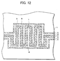
- the conductive film pattern 1 is formed in a meandering manner (what is called, a meander-type inductor) as shown in FIG. 12, area efficiency is lower than a case where the conductive film pattern 1 is formed in a spiral manner (what is called, a spiral inductor), but the inductor component is smaller, so that it is possible to heighten resonance frequency. Further, in the case where the conductive film pattern 1 is formed in a meandering manner the drawing wire is not required, so that the structure can be simplified.
- a meandering manner what is called, a meander-type inductor
- the inductance section is provided by using the spiral conductive film pattern 1 (wiring pattern) as described above, so that it is possible to obtain the strong inductance characteristic in a small area occupied by the inductance section.
- the conductive film pattern 1 can be provided not only by the deposition, the sputtering, and the printing, but also by using a wire etc. A shape, the number of times wound, thickness of the film, and width of a pattern (width of the conductive film) are set, as required, so as to obtain a desired inductance value.
- the p type silicon semiconductor substrate is used as the semiconductor substrate 4, and the p type impurity region 9 is formed on a surface (main surface) of the p type silicon semiconductor substrate.
- an n type silicon semiconductor substrate may be used as the semiconductor substrate 4, and an n type impurity region 9 may be formed on a surface (main surface) of the n type silicon semiconductor substrate.
- the impurity region 9 is a grounding potential layer, connected to the ground (grounded), which has low resistance.
- the impurity region 9 may have the same polarity as the semiconductor substrate 4, and may have an inverse polarity.
- FIG. 6 and FIG. 7 Another embodiment of the present invention is described based on FIG. 6 and FIG. 7 as follows. Note that, in the present embodiment, the same signs are given to components having the same functions as the components described in Embodiment 1, and descriptions thereof are omitted. In the present embodiment, differences between the present embodiment and Embodiment 1 will be described.
- FIG. 6 is a plan view showing a schematic structure of an inductance element formation section of a semiconductor device according to the present embodiment.
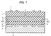
- FIG. 7 is a cross sectional view in line C-C' of the semiconductor device shown in FIG. 6. Note that, in FIG. 6, for the sake of convenience in description, the insulating films 5, 6, and 7 shown in FIG. 7 are not displayed, and patterns are given to the respective components. That is, in FIG. 6, the same patterns are given to the same components.
- the impurity region 9 is provided on the semiconductor substrate 4 so as to cover whole area under an area where the inductance section is formed. Further, in the semiconductor device, the conductive film 8 which grounds the impurity region 9 is provided in the vicinity of an area under the conductive film pattern 1 (wire) making up the inductance section so as to be formed along the conductive film pattern (wire) 1.
- the conductive film 8 is provided on an outside of the area where the conductive film pattern 1 is formed in the spiral manner (on an outside of an outline of the conductive film pattern 1), that is, the conductive film 8 is provided on an outside of an outermost line of the conductive film pattern 1 (wire) making up the spiral inductance section, in the vicinity of an area under the conductive film (conductive film pattern), so as not to be lapped by the conductive film pattern 1 and the connection wire 3.
- the impurity region 9 is provided only at (a) an area under the conductive film pattern 1 making up the inductance element, (b) an area under the connection wire 3 which serves as a drawing wire for connection of the inductance element, and (c) an area where the contact hole 10 for connecting the conductive film 8 to the impurity region 9.
- the conductive film 8 can be provided so as not to be lapped by the conductive film pattern 1 and the connection wire 3 at all. Therefore, it is possible to reduce the parasitic capacitance which occurs between the conductive film pattern 1/the connection wire 3 and the grounding area (grounding potential layer) further.
- two conductive films 8, as shown in FIG. 6 and FIG. 7, are provided.
- the two conductive films 8 are provided on the outside of an outermost line of the first conductive film pattern, and the outermost line is parallel to a direction in which respective terminals of the first conductive film pattern are drawn.
- the present embodiment is not limited to this, but a single conductive film 8 may be provided in any point around the conductive film pattern 1 making up the inductance section.
- the conductive film 8 is provided so that the impurity region 9 can be used as the grounding area (grounding potential layer), a particular limitation is not given to how the conductive film 8 is provided.
- the inductance element according to the present embodiment may also be provided directly in the semiconductor device by using the semiconductor substrate 4 making up the semiconductor device and other wires etc., while forming other components, for example, the transistor 20 etc. of the circuit section such as the integrated circuit at the same time, as shown in FIG. 4 and FIG. 5 concerning Embodiment 1. Further, the inductance element may be provided as a separate part from other circuit substrates.
- the inductance element according to the present invention includes an inductance section, provided above a semiconductor substrate via insulating films, which is composed of a first conductive film pattern setted to have a predetermined inductance value, wherein an impurity region, which has a grounding potential and a denser impurity than that of the semiconductor substrate, is provided on the semiconductor substrate so as to be positioned at least at an area under the first conductive film pattern.
- the impurity region is electrically connected to a grounded second conductive film pattern which is provided above the impurity region via the insulating substrates. It is preferable that the second conductive film pattern is provided so as not to be positioned at an area under the first conductive film pattern.
- the impurity region is electrically connected to the grounded second conductive film pattern which is provided above the impurity region via the insulating substrates, so that it is possible to make the impurity region grounded.
- the second conductive film pattern is provided so as not to be positioned at an area under the first conductive film pattern, so that the impurity region provided on the surface of the semiconductor substrate can be used as a grounding potential layer which reduces reflection and loss of a high frequency signal passing through the first conductive film pattern.
- a film thickness (distance) between the inductance section and a layer or an area which is used as the grounding potential layer so that it is possible to reduce the parasitic capacitance, compared with a conventional inductance element.
- the first conductive film pattern is electrically connected to a drawing wire, connecting to an external portion, which consists of a third conductive film pattern provided on an insulating film covering the second conductive film pattern, and it is preferable that the second conductive film pattern is provided so as not to be positioned at an area under the third conductive film pattern.
- the second conductive film pattern is provided so as not to be positioned at the area under the third conductive film pattern, so that it is possible to reduce the parasitic capacitance which occurs between the connection wire 3 and the grounding area (grounding potential layer). Thus, it is possible to improve the performance of the inductance element further.
- the inductance element according to the present invention includes: the second conductive film pattern provided above the impurity region via the first insulating film; the third conductive film pattern, provided above the second conductive film pattern via a second insulating film, which serves as a drawing wire for connection of the inductance section which is composed of the first conductive film pattern; and the inductance section, provided above the third conductive film pattern via a third insulating film, which is composed of the first conducive film pattern.
- the third conductive film pattern electrically connects the first conductive film pattern, for example, to an external circuit.
- the third conductive film pattern may be connected to a bonding wire, and may be connected to the external circuit via the boding wire.
- the first conductive film pattern is provided in a spiral manner.
- the first conductive film pattern may be provided in a meandering manner.
- the first conductive film pattern is, for example, connected to the drawing wire for connection which is composed of the third conductive film pattern, via a via-hole provided in an insulating film covering the drawing wire for connection.
- the second conductive film pattern is, for example, connected to the impurity region via a via-hole provided in an insulating film covering the impurity region.
- the second conductive film pattern is, for example, provided in the vicinity of the first conductive film pattern, with it along the first conductive film pattern, at least, so as not to be lapped by the first conductive film pattern.
- the drawing wire for connection (connection wire), which is composed of the third conductive film pattern, is drawn to the outside of the conductive film pattern, and the second conductive film pattern may be extended to the outside of the first conductive film pattern, so as not to be positioned at an area under the third conductive film pattern.
- connection wire which is composed of the third conductive film pattern
- the second conductive film pattern may be extended to the outside of the first conductive film pattern, so as not to be positioned at an area under the third conductive film pattern.
- the second conductive film pattern may be provided outside (outside an outermost line of) the first conductive film pattern, so as not to be positioned at an area under the third conductive film pattern, for example, the second conductive film pattern may be extended in a direction different from a direction in which the third conductive film pattern is drawn.
- the impurity region can be provided only at (a) an area below (under) the first conductive film pattern, (b) an area below (under) the third conductive film pattern which serves as the drawing wire for connection of the inductance element, and (c) an area where a contact hole (via-hole) for connecting the second conductive film pattern to the impurity region.
- the impurity region is provided below (under) the first conductive film pattern and the third conductive film pattern, so as to be formed along the first conductive film pattern and the third conductive film pattern.
- the inductance element is used, for example, with it provided in a semiconductor device.
- the semiconductor device according to the present invention is arranged so that the inductance element is internally provided.
- the semiconductor device is arranged so that the inductance element is internally provided, so that it is possible to reduce reflection and loss of a high frequency signal passing through the inductance section, which is brought about in the semiconductor substrate due to electromagnetic induction of a current applied to the inductance section of the inductance element, and it is pcssible to restrict decline of a Q value which indicates the performance of the inductance element with respect to frequency.
- the parasitic capacitance can be reduced, and it is possible to provide a semiconductor device having a high quality inductance characteristic.
- the semiconductor device having the inductance element therein can be arranged so that an integrated circuit such as an LSI is provided on the semiconductor substrate making up the inductance element. Further, the semiconductor device can be arranged so that a semiconductor substrate (inductance element) having the inductance section is provided on the semiconductor substrate on which the integrated circuit is provided. Alternatively, the semiconductor device can be arranged so that plural semiconductor substrates, which includes the semiconductor substrate having the inductance section, are provided on a semiconductor mounting portion of a lead frame, so as to store the semiconductor substrates in a single package. That is, the semiconductor device may be arranged so that the inductance element is provided directly in the semiconductor device, while forming other components at the same time, by using the semiconductor substrates and other wires etc. which make up the semiconductor device.
- the semiconductor device may be arranged so that the inductance element is provided as a separate part from other circuit substrates.
- the semiconductor device may be arranged so that the integrated circuit is not provided on the semiconductor substrate having the inductance section, and at least one semiconductor substrate, which has the integrated circuit therein, is provided additionally, and the additional semiconductor substrate and the inductance element, that is, the semiconductor substrate having the inductance section are stored in a single package and is sealed, so that the package is used as a multichip type semiconductor device.
- the semiconductor substrate (inductance element) having the inductance section is connected to a semiconductor substrate having an element area where the integrated circuit is provided, that is, to a silicon semiconductor substrate, and the semiconductor substrates are packaged.
- the packaged semiconductor substrates can serve as one chip which is provided in a miniature device such as a mobile communication device.
- passive elements such as a capacitor and a resistor are mounted on the semiconductor substrate having the inductance section is provided and the integrated circuit is not provided.
- a semiconductor device may be arranged by combining the semiconductor substrate having the passive elements with the semiconductor substrate having the integrated circuit.
- the semiconductor substrate making up the inductance element may be directly glued to the semiconductor substrate having the integrated circuit, by using an adhesive. Further, upon the foregoing combination, the semiconductor substrate having the integrated circuit may be connected to the semiconductor substrate making up the inductance element by a wire in accordance with wire bonding etc.
- a wire a TAB (Tape Automated Bonding) tape and a lead frame etc. can be used. By using these wires, it is possible to electrically connect both the semiconductor substrates.
- the semiconductor device is arranged so that the inductance element is separated from the semiconductor substrate having the integrated circuit, for example, from an integrated circuit formation portion (element formation portion) of the semiconductor substrate, at the grounding area, that is, at the impurity region, so that it is possible to prevent other elements from being influenced by noise.
- the inductance element and the semiconductor device having the inductance element according to the present invention can be widely applied to products which require the inductance element, for example, portable communication devices such as a cellular phone.
Landscapes
- Engineering & Computer Science (AREA)
- Power Engineering (AREA)
- Microelectronics & Electronic Packaging (AREA)
- Semiconductor Integrated Circuits (AREA)
- Coils Or Transformers For Communication (AREA)
Abstract
Description
Claims (16)
- An inductance element comprising an inductance section, provided above a semiconductor substrate (4) via insulating films (5, 6, 7), which is composed of a first conductive film pattern (1) setted to have a predetermined inductance value, wherein
an impurity region (9), which has a grounding potential and a denser impurity than that of the semiconductor substrate (4), is provided on the semiconductor substrate (4) so as to be positioned at least at an area under the first conductive film pattern (1). - The inductance element as set forth in claim 1, wherein:the impurity region (9) is electrically connected to a second conductive film pattern (8), provided above the impurity region (9) via one of the insulating films (5), which is grounded, andthe second conductive film pattern (8) is provided so as not to be positioned at the area under the first conductive film pattern (1).
- The inductance element as set forth in claim 2, wherein:the first conductive film pattern (1) is electrically connected to a drawing wire for external connection (3) which is composed of a third conductive film pattern provided on one of the insulating films (6) which covers the second conductive film pattern (8), andthe second conductive film pattern (8) is provided so as not to be positioned at an area under the third conductive film.
- The inductance element as set forth in claim 3, wherein:the drawing wire for external connection (3), which is composed of the third conductive film pattern, is drawn to an outside of the first conductive film pattern (1), andthe second conductive film pattern (8) is provided on the outside of the first conductive film pattern (1) so as not to be positioned at the area under the third conductive film pattern.
- The inductance element as set forth in claim 3 or 4, wherein the impurity region (9) is provided only at (a) the area under the first conductive film pattern (1), (b) the area under the third conductive film pattern, and (c) an area where a contact hole (10) for connecting the second conductive film pattern (8) to the impurity region (9) is provided.
- The inductance element as set forth in claim 1, wherein:the impurity region (9) is electrically connected to a second conductive film pattern (8), provided above the impurity region (9) via one of the insulating films (5), which is grounded, andthe second conductive film pattern (8) is provided with it along the first conductive film pattern (1) so as to be positioned in a vicinity of the area under the first conductive film pattern (1).
- The inductance element as set forth in claim 1, further comprising:a second conductive film pattern (8) provided above the impurity region (9) via a first insulating film (5);a third conductive film pattern, provided above the second conductive film pattern (8) via a second insulating film (6), which serves as a drawing wire for connection (3) of an inductance section which is composed of the first conductive film pattern (1); andthe inductance section, provided above the third conductive film pattern via a third insulating film (7), which is composed of the first conductive film pattern (1).
- The inductance element as set forth in claim 7, wherein the first conductive film pattern (1), the second conductive film pattern (8), the third conductive film pattern, and the impurity region (9) are electrically connected to each other via via-holes (10, 11, 25).
- The inductance element as set forth in any one of claims 1 to 8, wherein the first conductive film pattern (1) is provided in a spiral manner.
- The inductance element as set forth in claim 9, wherein:the impurity region (9) is electrically connected to a second conductive film pattern (8), provided above the impurity region (9) via one of the insulating films (5), which is grounded, andthe second conductive film pattern (8) is provided on an outside of an outermost line of the first conductive film pattern (1), the outermost line being parallel to a direction in which respective terminals of the first conductive film pattern (1) are drawn.
- The inductance element as set forth in claim 9, wherein:the impurity region (9) is electrically connected to a second conductive film pattern (8), provided above the impurity region (9) via one of the insulating films (5), which is grounded, andthe second conductive film pattern (8) is provided on an outside of an outermost line of the first conductive film pattern (1) so as to be provided in a direction different from a direction in which the third conductive film pattern is drawn.
- The inductance element as set forth in any one of claims 1, 2, and 6, wherein the conductive film pattern (1) is provided in a meandering manner.
- A semiconductor device comprising the inductance element as set forth in claim 1.
- The semiconductor device as set forth in claim 13, wherein the inductance element is internally provided.
- The semiconductor device as set forth in claim 14, wherein the semiconductor substrate, having the inductance section, includes a circuit section (20) of an integrated circuit thereon.
- An inductance element provided on a semiconductor substrate and comprising a conductive film pattern formed on an insulating film, said insulating film being disposed on said substrate, wherein said substrate includes a grounded impurity region formed at least in an area under the conductive film pattern.
Applications Claiming Priority (2)
| Application Number | Priority Date | Filing Date | Title |
|---|---|---|---|
| JP2001107730 | 2001-04-05 | ||
| JP2001107730A JP3579000B2 (en) | 2001-04-05 | 2001-04-05 | Semiconductor device |
Publications (3)
| Publication Number | Publication Date |
|---|---|
| EP1248297A2 true EP1248297A2 (en) | 2002-10-09 |
| EP1248297A3 EP1248297A3 (en) | 2004-09-08 |
| EP1248297B1 EP1248297B1 (en) | 2008-05-21 |
Family
ID=18960001
Family Applications (1)
| Application Number | Title | Priority Date | Filing Date |
|---|---|---|---|
| EP02251762A Expired - Lifetime EP1248297B1 (en) | 2001-04-05 | 2002-03-13 | Inductance element and semiconductor device |
Country Status (6)
| Country | Link |
|---|---|
| US (1) | US6661078B2 (en) |
| EP (1) | EP1248297B1 (en) |
| JP (1) | JP3579000B2 (en) |
| KR (1) | KR100475477B1 (en) |
| DE (1) | DE60226661D1 (en) |
| TW (1) | TW536807B (en) |
Cited By (1)
| Publication number | Priority date | Publication date | Assignee | Title |
|---|---|---|---|---|
| EP1445801A1 (en) * | 2003-02-07 | 2004-08-11 | STMicroelectronics S.A. | Integrated inductance and electronc devices comprising the same |
Families Citing this family (16)
| Publication number | Priority date | Publication date | Assignee | Title |
|---|---|---|---|---|
| JP3616605B2 (en) * | 2002-04-03 | 2005-02-02 | 沖電気工業株式会社 | Semiconductor device |
| WO2004047174A1 (en) * | 2002-11-21 | 2004-06-03 | Fujitsu Limited | Semiconductor integrated circuit device having high q inductance |
| JPWO2004107444A1 (en) * | 2003-05-29 | 2006-07-20 | 三菱電機株式会社 | Semiconductor device |
| US20050104158A1 (en) * | 2003-11-19 | 2005-05-19 | Scintera Networks, Inc. | Compact, high q inductor for integrated circuit |
| JP2006041357A (en) * | 2004-07-29 | 2006-02-09 | Fujikura Ltd | Semiconductor device and manufacturing method thereof |
| KR100759252B1 (en) * | 2005-06-30 | 2007-09-17 | 매그나칩 반도체 유한회사 | PSS and semiconductor device including same |
| JP4707056B2 (en) * | 2005-08-31 | 2011-06-22 | 富士通株式会社 | Integrated electronic component and integrated electronic component manufacturing method |
| JP4946219B2 (en) * | 2006-07-07 | 2012-06-06 | ソニー株式会社 | Variable inductor and semiconductor device using the same |
| JP4842052B2 (en) * | 2006-08-28 | 2011-12-21 | 富士通株式会社 | Inductor element and integrated electronic component |
| KR100725714B1 (en) * | 2006-08-29 | 2007-06-07 | 동부일렉트로닉스 주식회사 | Inductor and Inductor Manufacturing Method |
| US8212155B1 (en) * | 2007-06-26 | 2012-07-03 | Wright Peter V | Integrated passive device |
| JP2009302418A (en) * | 2008-06-17 | 2009-12-24 | Nec Electronics Corp | Circuit apparatus, and method of manufacturing the same |
| JP5598461B2 (en) * | 2011-12-05 | 2014-10-01 | ソニー株式会社 | Variable inductor and semiconductor device using the same |
| KR20190033314A (en) | 2017-09-21 | 2019-03-29 | 이삼형 | Pouch for easy to mix two contents |
| JP7529155B2 (en) * | 2021-05-31 | 2024-08-06 | 株式会社村田製作所 | Electronic Components |
| US20240355728A1 (en) * | 2023-04-21 | 2024-10-24 | Taiwan Semiconductor Manufacturing Company, Ltd. | Semiconductor structure |
Family Cites Families (5)
| Publication number | Priority date | Publication date | Assignee | Title |
|---|---|---|---|---|
| JPH06181289A (en) | 1992-12-14 | 1994-06-28 | Toshiba Corp | Semiconductor device |
| US5717243A (en) * | 1996-04-24 | 1998-02-10 | Harris Corporation | Integrated circuit with an improved inductor structure and method of fabrication |
| EP0940849A1 (en) * | 1998-03-05 | 1999-09-08 | Interuniversitair Micro-Elektronica Centrum Vzw | A low-loss conductive pattern on a substrate and a method for fabrication thereof |
| JP2000022085A (en) * | 1998-06-29 | 2000-01-21 | Toshiba Corp | Semiconductor device and manufacturing method thereof |
| JP4776752B2 (en) * | 2000-04-19 | 2011-09-21 | ルネサスエレクトロニクス株式会社 | Semiconductor device |
-
2001
- 2001-04-05 JP JP2001107730A patent/JP3579000B2/en not_active Expired - Lifetime
-
2002
- 2002-03-05 TW TW091104041A patent/TW536807B/en not_active IP Right Cessation
- 2002-03-06 US US10/090,766 patent/US6661078B2/en not_active Expired - Lifetime
- 2002-03-11 KR KR10-2002-0012922A patent/KR100475477B1/en not_active Expired - Fee Related
- 2002-03-13 DE DE60226661T patent/DE60226661D1/en not_active Expired - Fee Related
- 2002-03-13 EP EP02251762A patent/EP1248297B1/en not_active Expired - Lifetime
Cited By (2)
| Publication number | Priority date | Publication date | Assignee | Title |
|---|---|---|---|---|
| EP1445801A1 (en) * | 2003-02-07 | 2004-08-11 | STMicroelectronics S.A. | Integrated inductance and electronc devices comprising the same |
| FR2851078A1 (en) * | 2003-02-07 | 2004-08-13 | St Microelectronics Sa | INTEGRATED INDUCTANCE AND ELECTRONIC CIRCUIT INCORPORATING THE SAME |
Also Published As
| Publication number | Publication date |
|---|---|
| JP2002305246A (en) | 2002-10-18 |
| KR20020079381A (en) | 2002-10-19 |
| KR100475477B1 (en) | 2005-03-10 |
| TW536807B (en) | 2003-06-11 |
| US6661078B2 (en) | 2003-12-09 |
| EP1248297A3 (en) | 2004-09-08 |
| EP1248297B1 (en) | 2008-05-21 |
| DE60226661D1 (en) | 2008-07-03 |
| US20020145175A1 (en) | 2002-10-10 |
| JP3579000B2 (en) | 2004-10-20 |
Similar Documents
| Publication | Publication Date | Title |
|---|---|---|
| US6661078B2 (en) | Inductance element and semiconductor device | |
| US7859383B2 (en) | Spiral inductor with multi-trace structure | |
| US6501169B1 (en) | Semiconductor device which prevents leakage of noise generated in a circuit element forming area and which shields against external electromagnetic noise | |
| US7973246B2 (en) | Electronic component | |
| CN112103284B (en) | Chip components | |
| JP3792635B2 (en) | Electronic equipment | |
| US7551054B2 (en) | Electronic device and method of manufacturing the same | |
| US7531417B2 (en) | High performance system-on-chip passive device using post passivation process | |
| US6472738B2 (en) | Compound semiconductor device | |
| TWI236763B (en) | High performance system-on-chip inductor using post passivation process | |
| US7545036B2 (en) | Semiconductor device that suppresses variations in high frequency characteristics of circuit elements | |
| JP2000277693A (en) | Integrated circuit incorporating inductive elements and method of manufacturing such an integrated circuit | |
| US6781239B1 (en) | Integrated circuit and method of forming the integrated circuit having a die with high Q inductors and capacitors attached to a die with a circuit as a flip chip | |
| JP2004214561A (en) | Semiconductor device and manufacturing method thereof | |
| US20060038257A1 (en) | Semiconductor device which includes an inductor therein and a manufacturing method thereof | |
| JPH08330517A (en) | Integrated circuit device and resonant circuit | |
| JPH08172161A (en) | Inductor element, manufacturing method thereof, and monolithic microwave integrated circuit element using the same | |
| CN1685502B (en) | High-frequency signal transmission member | |
| JPH10154795A (en) | Inductor on semiconductor chip and its manufacturing method | |
| JP2006041357A (en) | Semiconductor device and manufacturing method thereof | |
| JPH06181289A (en) | Semiconductor device | |
| JP3535376B2 (en) | Microwave integrated circuit device | |
| JPH07183458A (en) | Semiconductor device | |
| US20250037919A1 (en) | Electronic component | |
| JP2006108323A (en) | Inductance element and manufacturing method thereof |
Legal Events
| Date | Code | Title | Description |
|---|---|---|---|
| PUAI | Public reference made under article 153(3) epc to a published international application that has entered the european phase |
Free format text: ORIGINAL CODE: 0009012 |
|
| AK | Designated contracting states |
Kind code of ref document: A2 Designated state(s): AT BE CH CY DE DK ES FI FR GB GR IE IT LI LU MC NL PT SE TR |
|
| AX | Request for extension of the european patent |
Free format text: AL;LT;LV;MK;RO;SI |
|
| PUAL | Search report despatched |
Free format text: ORIGINAL CODE: 0009013 |
|
| AK | Designated contracting states |
Kind code of ref document: A3 Designated state(s): AT BE CH CY DE DK ES FI FR GB GR IE IT LI LU MC NL PT SE TR |
|
| AX | Request for extension of the european patent |
Extension state: AL LT LV MK RO SI |
|
| 17P | Request for examination filed |
Effective date: 20041215 |
|
| AKX | Designation fees paid |
Designated state(s): DE FR GB IT NL |
|
| 17Q | First examination report despatched |
Effective date: 20050718 |
|
| GRAC | Information related to communication of intention to grant a patent modified |
Free format text: ORIGINAL CODE: EPIDOSCIGR1 |
|
| GRAP | Despatch of communication of intention to grant a patent |
Free format text: ORIGINAL CODE: EPIDOSNIGR1 |
|
| GRAS | Grant fee paid |
Free format text: ORIGINAL CODE: EPIDOSNIGR3 |
|
| GRAA | (expected) grant |
Free format text: ORIGINAL CODE: 0009210 |
|
| AK | Designated contracting states |
Kind code of ref document: B1 Designated state(s): DE FR GB IT NL |
|
| REG | Reference to a national code |
Ref country code: GB Ref legal event code: FG4D |
|
| REF | Corresponds to: |
Ref document number: 60226661 Country of ref document: DE Date of ref document: 20080703 Kind code of ref document: P |
|
| PLBE | No opposition filed within time limit |
Free format text: ORIGINAL CODE: 0009261 |
|
| STAA | Information on the status of an ep patent application or granted ep patent |
Free format text: STATUS: NO OPPOSITION FILED WITHIN TIME LIMIT |
|
| 26N | No opposition filed |
Effective date: 20090224 |
|
| GBPC | Gb: european patent ceased through non-payment of renewal fee |
Effective date: 20090313 |
|
| NLV4 | Nl: lapsed or anulled due to non-payment of the annual fee |
Effective date: 20091001 |
|
| REG | Reference to a national code |
Ref country code: FR Ref legal event code: ST Effective date: 20091130 |
|
| PG25 | Lapsed in a contracting state [announced via postgrant information from national office to epo] |
Ref country code: DE Free format text: LAPSE BECAUSE OF NON-PAYMENT OF DUE FEES Effective date: 20091001 |
|
| PG25 | Lapsed in a contracting state [announced via postgrant information from national office to epo] |
Ref country code: NL Free format text: LAPSE BECAUSE OF NON-PAYMENT OF DUE FEES Effective date: 20091001 |
|
| PG25 | Lapsed in a contracting state [announced via postgrant information from national office to epo] |
Ref country code: GB Free format text: LAPSE BECAUSE OF NON-PAYMENT OF DUE FEES Effective date: 20090313 Ref country code: FR Free format text: LAPSE BECAUSE OF NON-PAYMENT OF DUE FEES Effective date: 20091123 |
|
| PG25 | Lapsed in a contracting state [announced via postgrant information from national office to epo] |
Ref country code: IT Free format text: LAPSE BECAUSE OF NON-PAYMENT OF DUE FEES Effective date: 20090313 |