EP1248296A1 - Semiconductor laser element - Google Patents
Semiconductor laser element Download PDFInfo
- Publication number
- EP1248296A1 EP1248296A1 EP01963461A EP01963461A EP1248296A1 EP 1248296 A1 EP1248296 A1 EP 1248296A1 EP 01963461 A EP01963461 A EP 01963461A EP 01963461 A EP01963461 A EP 01963461A EP 1248296 A1 EP1248296 A1 EP 1248296A1
- Authority
- EP
- European Patent Office
- Prior art keywords
- layer
- facet
- current
- current blocking
- type
- Prior art date
- Legal status (The legal status is an assumption and is not a legal conclusion. Google has not performed a legal analysis and makes no representation as to the accuracy of the status listed.)
- Withdrawn
Links
Images




Classifications
-
- H—ELECTRICITY
- H01—ELECTRIC ELEMENTS
- H01S—DEVICES USING THE PROCESS OF LIGHT AMPLIFICATION BY STIMULATED EMISSION OF RADIATION [LASER] TO AMPLIFY OR GENERATE LIGHT; DEVICES USING STIMULATED EMISSION OF ELECTROMAGNETIC RADIATION IN WAVE RANGES OTHER THAN OPTICAL
- H01S5/00—Semiconductor lasers
- H01S5/10—Construction or shape of the optical resonator, e.g. extended or external cavity, coupled cavities, bent-guide, varying width, thickness or composition of the active region
- H01S5/16—Window-type lasers, i.e. with a region of non-absorbing material between the active region and the reflecting surface
-
- B—PERFORMING OPERATIONS; TRANSPORTING
- B82—NANOTECHNOLOGY
- B82Y—SPECIFIC USES OR APPLICATIONS OF NANOSTRUCTURES; MEASUREMENT OR ANALYSIS OF NANOSTRUCTURES; MANUFACTURE OR TREATMENT OF NANOSTRUCTURES
- B82Y20/00—Nanooptics, e.g. quantum optics or photonic crystals
-
- H—ELECTRICITY
- H01—ELECTRIC ELEMENTS
- H01S—DEVICES USING THE PROCESS OF LIGHT AMPLIFICATION BY STIMULATED EMISSION OF RADIATION [LASER] TO AMPLIFY OR GENERATE LIGHT; DEVICES USING STIMULATED EMISSION OF ELECTROMAGNETIC RADIATION IN WAVE RANGES OTHER THAN OPTICAL
- H01S5/00—Semiconductor lasers
- H01S5/20—Structure or shape of the semiconductor body to guide the optical wave ; Confining structures perpendicular to the optical axis, e.g. index or gain guiding, stripe geometry, broad area lasers, gain tailoring, transverse or lateral reflectors, special cladding structures, MQW barrier reflection layers
- H01S5/22—Structure or shape of the semiconductor body to guide the optical wave ; Confining structures perpendicular to the optical axis, e.g. index or gain guiding, stripe geometry, broad area lasers, gain tailoring, transverse or lateral reflectors, special cladding structures, MQW barrier reflection layers having a ridge or stripe structure
- H01S5/223—Buried stripe structure
- H01S5/2231—Buried stripe structure with inner confining structure only between the active layer and the upper electrode
-
- H—ELECTRICITY
- H01—ELECTRIC ELEMENTS
- H01S—DEVICES USING THE PROCESS OF LIGHT AMPLIFICATION BY STIMULATED EMISSION OF RADIATION [LASER] TO AMPLIFY OR GENERATE LIGHT; DEVICES USING STIMULATED EMISSION OF ELECTROMAGNETIC RADIATION IN WAVE RANGES OTHER THAN OPTICAL
- H01S2304/00—Special growth methods for semiconductor lasers
- H01S2304/04—MOCVD or MOVPE
-
- H—ELECTRICITY
- H01—ELECTRIC ELEMENTS
- H01S—DEVICES USING THE PROCESS OF LIGHT AMPLIFICATION BY STIMULATED EMISSION OF RADIATION [LASER] TO AMPLIFY OR GENERATE LIGHT; DEVICES USING STIMULATED EMISSION OF ELECTROMAGNETIC RADIATION IN WAVE RANGES OTHER THAN OPTICAL
- H01S5/00—Semiconductor lasers
- H01S5/10—Construction or shape of the optical resonator, e.g. extended or external cavity, coupled cavities, bent-guide, varying width, thickness or composition of the active region
- H01S5/16—Window-type lasers, i.e. with a region of non-absorbing material between the active region and the reflecting surface
- H01S5/164—Window-type lasers, i.e. with a region of non-absorbing material between the active region and the reflecting surface with window regions comprising semiconductor material with a wider bandgap than the active layer
-
- H—ELECTRICITY
- H01—ELECTRIC ELEMENTS
- H01S—DEVICES USING THE PROCESS OF LIGHT AMPLIFICATION BY STIMULATED EMISSION OF RADIATION [LASER] TO AMPLIFY OR GENERATE LIGHT; DEVICES USING STIMULATED EMISSION OF ELECTROMAGNETIC RADIATION IN WAVE RANGES OTHER THAN OPTICAL
- H01S5/00—Semiconductor lasers
- H01S5/10—Construction or shape of the optical resonator, e.g. extended or external cavity, coupled cavities, bent-guide, varying width, thickness or composition of the active region
- H01S5/16—Window-type lasers, i.e. with a region of non-absorbing material between the active region and the reflecting surface
- H01S5/168—Window-type lasers, i.e. with a region of non-absorbing material between the active region and the reflecting surface with window regions comprising current blocking layers
-
- H—ELECTRICITY
- H01—ELECTRIC ELEMENTS
- H01S—DEVICES USING THE PROCESS OF LIGHT AMPLIFICATION BY STIMULATED EMISSION OF RADIATION [LASER] TO AMPLIFY OR GENERATE LIGHT; DEVICES USING STIMULATED EMISSION OF ELECTROMAGNETIC RADIATION IN WAVE RANGES OTHER THAN OPTICAL
- H01S5/00—Semiconductor lasers
- H01S5/30—Structure or shape of the active region; Materials used for the active region
- H01S5/305—Structure or shape of the active region; Materials used for the active region characterised by the doping materials used in the laser structure
-
- H—ELECTRICITY
- H01—ELECTRIC ELEMENTS
- H01S—DEVICES USING THE PROCESS OF LIGHT AMPLIFICATION BY STIMULATED EMISSION OF RADIATION [LASER] TO AMPLIFY OR GENERATE LIGHT; DEVICES USING STIMULATED EMISSION OF ELECTROMAGNETIC RADIATION IN WAVE RANGES OTHER THAN OPTICAL
- H01S5/00—Semiconductor lasers
- H01S5/30—Structure or shape of the active region; Materials used for the active region
- H01S5/34—Structure or shape of the active region; Materials used for the active region comprising quantum well or superlattice structures, e.g. single quantum well [SQW] lasers, multiple quantum well [MQW] lasers or graded index separate confinement heterostructure [GRINSCH] lasers
- H01S5/343—Structure or shape of the active region; Materials used for the active region comprising quantum well or superlattice structures, e.g. single quantum well [SQW] lasers, multiple quantum well [MQW] lasers or graded index separate confinement heterostructure [GRINSCH] lasers in AIIIBV compounds, e.g. AlGaAs-laser, InP-based laser
- H01S5/34313—Structure or shape of the active region; Materials used for the active region comprising quantum well or superlattice structures, e.g. single quantum well [SQW] lasers, multiple quantum well [MQW] lasers or graded index separate confinement heterostructure [GRINSCH] lasers in AIIIBV compounds, e.g. AlGaAs-laser, InP-based laser with a well layer having only As as V-compound, e.g. AlGaAs, InGaAs
Definitions
- the present invention relates to a high-power semiconductor laser having a current noninjected region in the vicinity of an end face (facet).
- the invention enhances a facet Catastrophic Optical Damage level higher and provides high reliability in long-term continuous operations.
- a semiconductor laser device is utilized in various fields such as an excitation light source for a light amplifier used in the field of communications. These lasers are required for high power operations. However, there is a problem that it is difficult to obtain the semiconductor laser having enough life for carrying out the high power operations.
- facet COD Catastrophic Optical Damage
- the COD is caused by the following steps. First, the non-radiative recombination is caused by defects produced in the vicinity of the facet. This results in an increase of the temperature. In addition, due to the temperature increase, the width of band gap is decreased and light absorption occurs, resulting in a vicious cycle of further temperature rise due to this. These steps induce melting of the facet and light output is deteriorated. Finally, a non-reversible destruction occurs.
- the facet COD it becomes important to reinforce the facet for obtaining the high-power semiconductor laser, in terms of preventing the facet COD.
- As one means for preventing the facet COD there is a method in which no current is injected in the vicinity of the facet. In this case, since a current injection is suppressed in the vicinity of the facet, the vicinity of the facet becomes non-excitation state. Because of this, the non-radiative recombination is suppressed, which enables to improve the facet COD level.
- no current is injected in the facet by forming an insulating film such as SiN under an electrode formed on the facet, no current is injected in the facet by forming a current blocking layer comprising a semiconductor layer on the facet, and no current is injected in the facet by carrying out ion implantation in the vicinity of the facet.
- the method causes damage to the semiconductor laser device, in which no current is injected in the facet by carrying out ion implantation in the vicinity of the facet. Furthermore, all these facet current blocking structures are formed at a distance from a waveguide layer.
- the current wraparound is considered to cause serious influence as the distance between the current blocking structure and the active layer increases. In the case where the influence of the current wraparound becomes serious even if the current blocking structure is formed on the facet, current is wrapped around the facet, resulting in function degradation of the facet current blocking structure. Consequently, in consideration of the current wraparound, it is necessary to form wide facet current blocking region.
- any conventional methods described above are not necessarily preferable when forming a current blocking structure in the vicinity of the facet.
- An object of the invention is to provide a semiconductor laser device having high facet COD level, and high reliability in long-term continuous operations, by providing a current blocking structure in the vicinity of the facet. According to the structure, fabrication processes become easy, no damage are caused to the semiconductor laser device, and the property deterioration can be minimized.
- the invention relates to a semiconductor laser device comprising:
- the first current blocking layers between which the stripe-shaped current injected region extending in the resonator direction is interposed, and the second current blocking layer, which is formed in order that no current is injected in one side or both sides of the vicinity of the facet, are made of the same layer, namely they are of the same composition and of the same film thickness. Because of this, fabrication processes become easy without increasing the number of processing steps compared with the conventional method. Consequently, the current blocking structure can be provided in the vicinity of the facet without damaging the semiconductor laser device. Accordingly, it is possible to provide the semiconductor laser device having high facet COD level and high reliability in long-term continuous operations. Not only the front facet but also the rear facet may be provided with the current blocking layer. One of both side portions of the second current blocking layer reaches the facet.
- a refractive index waveguide structure can be formed by an equivalent refractive index difference between the current injected region and the region of the current blocking layers. Further, a carrier blocking layer having larger energy gap than that of the waveguide layer is provided between the active layer and the waveguide layers, thereby a carrier is confined and a waveguide mode in the epitaxial direction can be expanded. Consequently, the facet COD level can be further improved by suppressing light intensity concentrated on the facet active layer.
- the first and second current blocking layers are formed inside the waveguide layer.
- the first and second current blocking layers may be formed in adjacent to the waveguide layer. In this case, when the width of the second current blocking layer is too large, waveguide loss is increased. Because of this, the second current blocking layer is desired to have a width within the range of 2 to 25 ⁇ m in practical use.
- the waveguide mode profile in the vicinity of the facet can be shifted from the active layer by the use of the low refractive index layer in the vicinity of the facet. Accordingly, the beam energy density near the active layer in the vicinity of the facet can be reduced, and it is possible to provide the semiconductor laser device having substantially improved facet COD level and high reliability in long-term continuous operations. Further, since the waveguide layers are formed in the vicinity of the active layer, influence caused by the current wraparound into the active layer can be reduced by providing the facet current blocking structure in the waveguide layers.
- the current blocking region necessary for ensuring improvement of the facet COD level and high reliability in long-term continuous operations can be narrower compared with the case where the current blocking structure is provided over the waveguide layers.
- influence due to light absorption can be decreased, resulting in reducing degradation of the properties (threshold current, slope efficiency, temperature characteristic, or the like) of the semiconductor laser device.
- the active layer comprises InGaAs and the waveguide layers are made of GaAs not including Al.
- GaAs not including Al for forming a waveguide layer by the use of InGaAs for forming quantum wells of the active layer. Because a regrowing interface is not subject to oxidation during the formation processes of the current blocking layer, stability of processes can be achieved so that fine film can be formed. The reduction of electrical resistance and thermal resistance can be accomplished by using a waveguide layer made of GaAs not including Al.
- a waveguide mode in the vicinity of the facet is influenced by the layer.
- the waveguide mode can be controlled by changing position, distance from the face and refractive index of the current blocking layer in the vicinity of the facet imbedded in the waveguide layer.
- the beam energy density near the active layer is represented by a light confinement factor ⁇ .
- ⁇ a light confinement factor
- position, width and refractive index of the current blocking layer in the vicinity of the facet are designed to satisfy the relationship between a light confinement factor ⁇ 1d Injection at the current injected region obtained through one dimensional slab waveguide path in the film thickness direction and a light confinement factor ⁇ 1d Non-injection in the film thickness direction at the current noninjected region in the vicinity of the facet as follows: ⁇ 1d Injection > ⁇ 1d Non-injection
- the light confinement factor ⁇ 1d Injection at the current injected region shows 0.0084
- the light confinement factor ⁇ 1d Non-injection in the film thickness direction at the current noninjected region in the vicinity of the facet shows 0.0071. Consequently, the beam energy density near the active layer in the vicinity of the facet, can be reduced.
- the light confinement factor ⁇ of one dimensional slab waveguide path used herein is defined as the following formula. wherein E(x) is an electric field in the film thickness direction, A and B are a maximum value and a minimum value of electric field coordinates, respectively. Further, a and b are values determined by an interface of the active layer.
- the waveguide mode beams propagate dynamically.
- the state in which the waveguide mode is influenced by the current blocking layer in the vicinity of the facet can be analyzed by e.g. a computer simulation using the beam propagation method.
- the position, width, and refractive index of the current blocking layer in the vicinity of the facet, which is imbedded in the waveguide layer are designed to satisfy the relationship between a light confinement factor ⁇ 2d Injection at the current injected region and a light intensity rate ⁇ 2d Facets at the active layer in the front facet with respect to a propagation mode when propagating the waveguide mode at a current injected region into a current noninjected region by the beam propagation method as follows: ⁇ 2d Injection > ⁇ 2d Facet
- Fig. 7 is a graph of an analysis obtained by a computer simulation (BPM CAD produced by Optiwave Corporation) using the beam propagation method.
- BPM CAD produced by Optiwave Corporation
- an analysis is carried out on the relationship between a light intensity rate (light confinement factor) ⁇ of the active layer with respect to the propagation mode at the side portion (reference numeral 23a in Fig.
- the light confinement factor ⁇ used herein is defined as the following formula. wherein E(x, y) is an electric field, (A, B) and (C, D) are a maximum value and a minimum value of electric field coordinates, respectively, and (a, b) and (c, d) are values determined by an interface of the active layer.
- the light confinement factor becomes a minimum value when the current blocking layer on the facet has a width of about 5 ⁇ m or 15 ⁇ m. It should be noted that the optimum value of the width of the current blocking layer in the vicinity of the facet is designed as necessary depending on the layer structure in order to minimize the light confinement factor at facets. Further, the width of the current blocking layer, which minimizes the light confinement factor, is varied by changing position, width and refractive index of the current blocking layer in the vicinity of the facet.
- Fig. 1A is a perspective view of an example of a semiconductor laser device according to the invention.
- Fig. 2 shows a current blocking layer 23 according to the invention by virtual dividing the layer configuration for the sake of clarity.
- Figs. 3A-3C are cross sectional views of Fig. 2.
- Fig. 3A is a cross section taken along the line A-A' in a direction at right angles to the resonator length direction of the laser and located at a distance from an emitting facet (front facet) and a rear facet.
- Fig. 3B shows the vicinity of the emitting facet taken along the cross sectional line B-B' parallel to the line A-A'.
- Fig. 3C is a cross section taken along the line C-C' which is almost center of stripes in which light waveguides in the resonator length direction.
- a buffer layer 32, an n-side cladding layer 31, an n-side waveguide layer 30, an active layer region 35, a p-side waveguide layer 24, a current blocking layer 23, a p-side waveguide layer 22, a p-side cladding layer 21, and a p-side cap layer 20 are formed on a n-GaAs substrate 33.
- the active layer region 35 comprises an n-side carrier blocking layer 29, an n-side side barrier layer 28, an active layer composed of quantum well layers and a barrier layer for interpolating these, a p-side side barrier layer 26, and a p-side carrier blocking layer 25.
- the current blocking layer 23 herein is provided in both sides of the stripe to determine a stripe S in the resonator length direction. Also, in the vicinity of a front facet 40 and a rear facet 41, the current blocking layer is provided to transverse the stripe S.
- FIGs. 4A-4C show cross sectional portions taken along the line A-A' in Fig. 2 in the order of fabrication steps.
- Fig. 4A first, an n-type (1 ⁇ 10 23 m -3 ) buffer layer 32 made of GaAs (0.5 ⁇ m), an n-type (1 ⁇ 10 24 m -3 ) cladding layer 31 made of Al 0.09 Ga 0.91 As (2.5 ⁇ m), an n-type (1 ⁇ 10 23 m -3 ) waveguide layer 30 made of GaAs (0.45 ⁇ m), an n-type (1 ⁇ 10 24 m -3 ) carrier blocking layer 29 made of Al 0.4 Ga 0.6 As (0.02 ⁇ m) , a side barrier layer 28 made of Al 0.1 Ga 0.9 As (0.
- an active layer 27 comprising two quantum well layers made of In 0.18 Ga 0.82 As (0.007 ⁇ m/one) and a barrier layer made of Al 0.1 Ga 0.9 As (0.006 ⁇ m) for interpolating the quantum well layers, a side barrier layer 26 made of Al 0.1 Ga 0.9 As (0.05 ⁇ m), a p-type (1 ⁇ 10 24 m -3 ) carrier blocking layer 25 made of Al 0.4 Ga 0.6 As (0.02 ⁇ m), and a p-type (1 ⁇ 10 24 m -3 ) waveguide layer 24 made of GaAs (0.1 ⁇ m) are successively formed on an n-type (1 ⁇ 10 23 m -3 )-GaAs substrate 33.
- MOCVD Metal Organic Chemical Vapor Deposition
- MBE Molecular Beam Epitaxial
- the substrate in which crystal growth is carried out in this way is taken out from the crystal growth apparatus and put into e.g. the electron beam vapor apparatus, thereby forming a mask 34 made of e.g. SiO 2 on an entire surface.
- the mask is removed except the central region by photolithography technique to form a stripe-shaped window, thereby forming a stripe-shaped mask 34.
- the mask in the vicinity of the facet is removed so as to form a current noninjected region on the facet. Since the mask 34 is extremely thin, it can be formed by conventional photolithography technique with high accuracy and improved reproducibility.
- the substrate having the mask 34 is replaced into the crystal growth apparatus to selectively grow a current blocking layer 23 made of an n-type (1 ⁇ 10 24 m -3 ) Al 0.09 Ga 0.91 As (0.18 ⁇ m) on a p-type (1 ⁇ 10 24 m -3 ) waveguide layer 24.
- the layer structure having no crystal growth can be obtained in the region attached with the mask 34.
- the mask 34 is removed by e.g. hydrofluoric acid solution.
- the current blocking layer may have such a layer structure having two layers or more. Further, after forming the current blocking layer on the entire surface, only the central region to be applied with a current may be removed by etching. In this way, the first current blocking layers and the second current blocking layer can be formed at the same time as the same layer.
- an upper p-type (1 ⁇ 10 23 m -3 ) waveguide layer 22 made of GaAs (0.35 ⁇ m), a p-type (1 ⁇ 10 24 m -3 ) cladding layer 21 made of Al 0.32 Ga 0.68 As (0.78 ⁇ m), and a cap layer 20 made of a p-type (1 ⁇ 10 24 m -3 )-GaAs (1.4 ⁇ m) are successively formed.
- one example of the semiconductor laser device of the invention can be obtained as shown in Fig. 2. Thereafter, an electrode is formed on the substrate and the cap layer 20 and a current is applied thereto, thereby laser oscillation can be performed by a carrier injection.
- a semiconductor laser device is provided with the current blocking layer in the waveguide layer in the vicinity of the facet.
- a light confinement factor ⁇ 1d Injection in the film thickness direction is fixed without depending on the resonator length direction.
- a light confinement factor ⁇ 1d Non-injection in the film thickness direction can be made smaller than the ⁇ 1d Injection by changing position, width, and refractive index of the second current blocking layer.
- a light intensity rate ⁇ 2d Facet in the active layer on the front facet with respect to propagation mode can be made smaller than a ⁇ 2d Injection by changing position, width, and refractive index of the second current blocking layer.
- the ⁇ 2d Facet can be made smaller than the ⁇ 2d Injection as shown in Fig. 7, and also, the ⁇ 2d Facet can be further decreased by selecting the width of the current blocking layer in order that the ⁇ 2d Facet in the vicinity of the active layer on the facet takes on values between adjacent inflection points including a minimum value.
- the position of the current blocking layer is not limited to the inside of the waveguide layer and it may be adjacent to the waveguide layer.
- the semiconductor laser device thus structured since a current injection in the vicinity of the facet is suppressed, the vicinity of the facet is in the state of non-excitation. Because of this, non-radiative recombination is suppressed, which enables to improve the facet COD level.
- the semiconductor laser device of the invention may have a ridge structure in which the active region is sandwiched between the current blocking layers.
- first current blocking layers and the second current blocking layer may be continuous as described in the embodiment, or they may be partially discontinuous to the extent to which properties are not deteriorated.
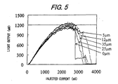
- Fig. 5 shows the state of light output when an overcurrent is applied to the semiconductor laser device obtained by the above-described way.
- some samples are prepared, which has various widths X of the current blocking layer crossing the stripe in the vicinity of the facet imbedded in the waveguide layer. In the vicinity of the facet, one edge portion of the current blocking layer comes in contact with the facet and remaining edge portions are placed in the location at a distance of x from the facet in the resonator length direction.
- COD occurs during the passage of a current.
- Figs. 6A-6B show results obtained by measurement of an injected current changed over time, where the environmental temperature at 70°C is used and an injection current is controlled to output fixed laser light.
- Fig. 6A shows the result regarding the semiconductor laser device having no current blocking layer in the vicinity of the facet. Since operation is carried out under the state in which a current is controlled to make fixed output, a current is increased in the case of deterioration. Referring to Fig. 6A, it can be found that the device is deteriorated in early stage with regard to the semiconductor laser device having no current blocking layer in the vicinity of the facet.
- the invention is not limited to the above mentioned embodiments, and applicable to semiconductor lasers having various structures and compositions.
Landscapes
- Physics & Mathematics (AREA)
- Optics & Photonics (AREA)
- General Physics & Mathematics (AREA)
- Chemical & Material Sciences (AREA)
- Engineering & Computer Science (AREA)
- Nanotechnology (AREA)
- Condensed Matter Physics & Semiconductors (AREA)
- Electromagnetism (AREA)
- Biophysics (AREA)
- Crystallography & Structural Chemistry (AREA)
- Life Sciences & Earth Sciences (AREA)
- Geometry (AREA)
- Semiconductor Lasers (AREA)
Abstract
Description


Claims (20)
- A semiconductor laser device comprising:wherein the first current blocking layers and the second current blocking layer are made of the same layer, and a refractive index waveguide structure is formed by an equivalent refractive. index difference between the current injected region and regions of the first and second current blocking layers.an active layer;an n-type waveguide layer;a p-type waveguide layer,the active layer being interposed between the n-type and p-type waveguide layers;n-type and p-type cladding layers formed so that outsides of the n-type and p-type waveguide layers are interposed therebetween;first current blocking layers formed to define a stripe-shaped current injected region extending in a direction where a front facet of the device from which a laser light is emitted and a rear facet opposing thereto are connected; anda second current blocking layer formed to transverse the stripe-shaped current injected region in a vicinity of the front facet,
- The semiconductor laser device of claim 1, wherein a carrier blocking layer is provided between the active layer and the p-type waveguide layer and/or between the active layer and the n-type waveguide layer, and the carrier blocking layer has larger energy gap than that of the waveguide layer.
- The semiconductor device of claim 1 or 2, wherein the first and second current blocking layers are formed inside the p-type waveguide layer and/or the n-type waveguide layer.
- The semiconductor device of claim 1 or 2, wherein the first and second current blocking layers are formed in adjacent to the p-type waveguide layer and/or the n-type waveguide layer.
- The semiconductor laser device of claim 3 or 4, wherein the active layer comprises InGaAs and the waveguide layers comprise GaAs and are free of Al.
- The semiconductor laser device of claim 3 or 4, wherein the active layer is composed of multiple layers comprising an InGaAsP layer, and the waveguide layers comprise GaAs and are free of Al.
- The semiconductor laser device of any one of claims 1 to 6, wherein the second current blocking layer is formed so that the following relationship is fulfilled:
- The semiconductor laser device of any one of claims 1 to 7, wherein the second current blocking layer is formed so that the following relationship is fulfilled:
- The semiconductor laser device of claim 9, wherein position, thickness and width of the second current blocking layer are defined so that the Γ2d Facet exists between adjacent inflection points including a minimum value.
- The semiconductor laser device of any one of claims 3 to 5, wherein the second current blocking layer has a width within the range of 2 to 25µm.
- A semiconductor laser device comprising:wherein the second current blocking layer is formed so that the following relationship is fulfilled:an active layer;an n-type waveguide layer;a p-type waveguide layer,the active layer being interposed between the n-type and p-type waveguide layers;n-type and p-type cladding layers formed so that outsides of the n-type and p-type waveguide layers are interposed therebetween;first current blocking layers formed to define a stripe-shaped current injected region extending in a direction where a front facet of the device from which a laser light is emitted and a rear facet opposing thereto are connected; anda second current blocking layer formed to transverse the stripe-shaped current injected region in a vicinity of the front facet,
- A semiconductor laser device comprising:wherein the second current blocking layer is formed so that the following relationship is fulfilled:an active layer;an n-type waveguide layer;a p-type waveguide layer,the active layer being interposed between the n-type and p-type waveguide layers;n-type and p-type cladding layers formed so that outsides of the n-type and p-type waveguide layers are interposed therebetween;first current blocking layers formed to define a stripe-shaped current injected region extending in a direction where a front facet of the device from which a laser light is emitted and a rear facet opposing thereto are connected; anda second current blocking layer formed to transverse the stripe-shaped current injected region in a vicinity of the front facet,
- The semiconductor laser device of claim 12, wherein position, thickness and width of the second current blocking layer are defined so that the Γ2d Facet exists between adjacent inflection points including a minimum value.
- The semiconductor laser device of any one of claims 11 to 13, wherein the second current blocking layer has a width within the range of 2 to 25µm.
- The semiconductor laser device of any one of claims 11 to 14, wherein a refractive index waveguide structure is formed by an equivalent refractive index difference between the current injected region and regions of the first and second current blocking layers.
- The semiconductor laser device of any one of claims 11 to 15, wherein a carrier blocking layer is provided between the active layer and the p-type waveguide layer and/or between the active layer and the n-type waveguide layer, and the carrier blocking layer has larger energy gap than that of the waveguide layer.
- The semiconductor laser device of any one of claims 11 to 15, the first and second current blocking layers are formed inside the p-type waveguide layer and/or the n-type waveguide layer.
- The semiconductor laser device of any one of claims 11 to 17, wherein the first and second current blocking layers are formed in adjacent to the p-type waveguide layer and/or the n-type waveguide layer.
- The semiconductor laser device of claim 17 or 18, wherein the active layer comprises InGaAs and the waveguide layers comprise GaAs and are free of Al.
- The semiconductor laser device of claim 17 or 18, wherein the active layer is composed of multiple layers comprising an InGaAsP layer, and the waveguide layers comprise GaAs and are free of Al.
Applications Claiming Priority (3)
| Application Number | Priority Date | Filing Date | Title |
|---|---|---|---|
| JP2000274013 | 2000-09-08 | ||
| JP2000274013 | 2000-09-08 | ||
| PCT/JP2001/007724 WO2002021578A1 (en) | 2000-09-08 | 2001-09-06 | Semiconductor laser element |
Publications (2)
| Publication Number | Publication Date |
|---|---|
| EP1248296A1 true EP1248296A1 (en) | 2002-10-09 |
| EP1248296A4 EP1248296A4 (en) | 2006-05-24 |
Family
ID=18759850
Family Applications (1)
| Application Number | Title | Priority Date | Filing Date |
|---|---|---|---|
| EP01963461A Withdrawn EP1248296A4 (en) | 2000-09-08 | 2001-09-06 | Semiconductor laser element |
Country Status (5)
| Country | Link |
|---|---|
| US (1) | US6822990B2 (en) |
| EP (1) | EP1248296A4 (en) |
| JP (1) | JP3974852B2 (en) |
| CN (1) | CN1204665C (en) |
| WO (1) | WO2002021578A1 (en) |
Families Citing this family (8)
| Publication number | Priority date | Publication date | Assignee | Title |
|---|---|---|---|---|
| US6798815B2 (en) * | 2002-04-24 | 2004-09-28 | Bookham Technology Plc | High power semiconductor laser diode and method for making such a diode |
| JP3911461B2 (en) * | 2002-08-29 | 2007-05-09 | シャープ株式会社 | Semiconductor laser device and manufacturing method thereof |
| GB2471266B (en) * | 2009-06-10 | 2013-07-10 | Univ Sheffield | Semiconductor light source and method of fabrication thereof |
| EP2453535B1 (en) | 2009-07-06 | 2021-05-05 | Furukawa Electric Co., Ltd. | Method for manufacturing semiconductor optical device, method for manufacturing semiconductor optical laser element, and semiconductor optical device |
| JP5579096B2 (en) * | 2011-02-14 | 2014-08-27 | 古河電気工業株式会社 | Semiconductor laser device and communication system |
| JP7406487B2 (en) * | 2018-07-27 | 2023-12-27 | ヌヴォトンテクノロジージャパン株式会社 | semiconductor laser device |
| CN112260060B (en) * | 2020-12-22 | 2021-03-09 | 武汉敏芯半导体股份有限公司 | Distributed feedback laser |
| JP2022115255A (en) * | 2021-01-28 | 2022-08-09 | ウシオ電機株式会社 | Nitride semiconductor light-emitting element |
Family Cites Families (13)
| Publication number | Priority date | Publication date | Assignee | Title |
|---|---|---|---|---|
| US4799228A (en) * | 1985-08-23 | 1989-01-17 | Kabushiki Kaisha Toshiba | Transverse-mode stabilized semiconductor laser diode with slab-coupled waveguide |
| JPS6251281A (en) | 1985-08-30 | 1987-03-05 | Nec Corp | Semiconductor laser |
| DE68918884T2 (en) * | 1988-03-14 | 1995-03-16 | Toshiba Kawasaki Kk | Semiconductor laser device. |
| JPH02125488A (en) | 1988-07-22 | 1990-05-14 | Mitsubishi Electric Corp | Semiconductor laser device |
| US5181218A (en) * | 1988-12-14 | 1993-01-19 | Kabushiki Kaisha Toshiba | Manufacturing method of semiconductor laser with non-absorbing mirror structure |
| JP2550717B2 (en) | 1989-08-23 | 1996-11-06 | 日本電気株式会社 | Method for manufacturing semiconductor laser device |
| JPH03126283A (en) * | 1989-10-11 | 1991-05-29 | Toshiba Corp | Manufacture of window-structured semiconductor laser element |
| JPH0590706A (en) | 1991-09-26 | 1993-04-09 | Anritsu Corp | Semiconductor laser element |
| JPH06188507A (en) | 1992-12-16 | 1994-07-08 | Matsushita Electric Ind Co Ltd | Quantum wire semiconductor laser and manufacturing method thereof |
| JP2879875B2 (en) | 1993-01-11 | 1999-04-05 | ローム株式会社 | Semiconductor laser device and method of manufacturing the same |
| JPH06251281A (en) | 1993-02-23 | 1994-09-09 | King Tsushin Kogyo Kk | Machine guard system |
| JPH11154775A (en) | 1997-09-18 | 1999-06-08 | Mitsui Chem Inc | Manufacture of semiconductor laser |
| EP1104057B1 (en) * | 1999-11-19 | 2005-07-27 | Fuji Photo Film Co., Ltd. | High-power semiconductor laser device having current confinement structure and index-guided structure |
-
2001
- 2001-09-06 JP JP2002525901A patent/JP3974852B2/en not_active Expired - Lifetime
- 2001-09-06 EP EP01963461A patent/EP1248296A4/en not_active Withdrawn
- 2001-09-06 US US10/129,550 patent/US6822990B2/en not_active Expired - Lifetime
- 2001-09-06 CN CNB018035345A patent/CN1204665C/en not_active Expired - Lifetime
- 2001-09-06 WO PCT/JP2001/007724 patent/WO2002021578A1/en not_active Ceased
Also Published As
| Publication number | Publication date |
|---|---|
| WO2002021578A1 (en) | 2002-03-14 |
| US6822990B2 (en) | 2004-11-23 |
| JPWO2002021578A1 (en) | 2004-01-15 |
| CN1204665C (en) | 2005-06-01 |
| JP3974852B2 (en) | 2007-09-12 |
| US20020171094A1 (en) | 2002-11-21 |
| EP1248296A4 (en) | 2006-05-24 |
| CN1394372A (en) | 2003-01-29 |
Similar Documents
| Publication | Publication Date | Title |
|---|---|---|
| EP0006723B1 (en) | Stripe offset geometry in injection lasers to achieve transverse mode control | |
| KR100243417B1 (en) | High power semiconductor laser with Al double holding structure | |
| JP2003101139A (en) | End surface emitting semiconductor laser and semiconductor laser module | |
| US6661822B1 (en) | Semiconductor light emitting device and method of manufacturing the same | |
| JPH0656906B2 (en) | Semiconductor laser device | |
| EP0660472A2 (en) | Semiconductor laser device | |
| JP3786907B2 (en) | Semiconductor light emitting device and manufacturing method thereof | |
| KR19990072352A (en) | Self-pulsation type semiconductor laser | |
| KR20010007396A (en) | Semiconductor laser | |
| US7167489B2 (en) | GaN-based semiconductor laser device | |
| US6822990B2 (en) | Semiconductor laser device | |
| US6567444B2 (en) | High-power semiconductor laser device in which near-edge portions of active layer are removed | |
| US7251381B2 (en) | Single-mode optical device | |
| JP3339486B2 (en) | Semiconductor laser, manufacturing method thereof, optical module and optical communication system using semiconductor laser | |
| EP0589727A2 (en) | Semiconductor laser device | |
| JP3658048B2 (en) | Semiconductor laser element | |
| KR100789309B1 (en) | Semiconductor laser | |
| GB2406968A (en) | Control of output beam divergence in a semiconductor laser | |
| JP3645320B2 (en) | Semiconductor laser element | |
| JPH0983070A (en) | Semiconductor laser device | |
| EP4220875A1 (en) | Semiconductor laser device | |
| JP2010123726A (en) | Semiconductor laser and manufacturing method thereof | |
| JPH10209553A (en) | Semiconductor laser device | |
| US7050472B2 (en) | Semiconductor laser device and method for manufacturing the same | |
| KR100759802B1 (en) | Flush Peak Waveguide Laser Diode |
Legal Events
| Date | Code | Title | Description |
|---|---|---|---|
| PUAI | Public reference made under article 153(3) epc to a published international application that has entered the european phase |
Free format text: ORIGINAL CODE: 0009012 |
|
| 17P | Request for examination filed |
Effective date: 20020529 |
|
| AK | Designated contracting states |
Kind code of ref document: A1 Designated state(s): AT BE CH CY DE DK ES FI FR GB GR IE IT LI LU MC NL PT SE TR |
|
| RBV | Designated contracting states (corrected) |
Designated state(s): AT BE CH CY DE FR GB LI |
|
| RAP1 | Party data changed (applicant data changed or rights of an application transferred) |
Owner name: MITSUI CHEMICALS, INC. |
|
| A4 | Supplementary search report drawn up and despatched |
Effective date: 20060412 |
|
| RIC1 | Information provided on ipc code assigned before grant |
Ipc: H01S 5/20 20060101ALI20060406BHEP Ipc: H01L 25/00 20060101AFI20020321BHEP Ipc: H01S 5/16 20060101ALI20060406BHEP |
|
| 17Q | First examination report despatched |
Effective date: 20090428 |
|
| STAA | Information on the status of an ep patent application or granted ep patent |
Free format text: STATUS: THE APPLICATION IS DEEMED TO BE WITHDRAWN |
|
| 18D | Application deemed to be withdrawn |
Effective date: 20150401 |